
 Open Access Article
 This Open Access Article is licensed under a Creative Commons Attribution-Non Commercial 3.0 Unported Licence
Modifications of the CZTSe/Mo back-contact interface by plasma treatments†
Wenjian Chen *a,
Teoman Taskesena,
David Nowaka,
Ulf Mikolajczaka,
Mohamed H. Sayeda,
Devendra Pareeka,
Jörg Ohlanda,
Thomas Schnabelb,
Erik Ahlswedeb,
Dirk Hauschildcde,
Lothar Weinhardtcde,
Clemens Heskecde,
Jürgen Parisia and
Levent Gütaya
*a,
Teoman Taskesena,
David Nowaka,
Ulf Mikolajczaka,
Mohamed H. Sayeda,
Devendra Pareeka,
Jörg Ohlanda,
Thomas Schnabelb,
Erik Ahlswedeb,
Dirk Hauschildcde,
Lothar Weinhardtcde,
Clemens Heskecde,
Jürgen Parisia and
Levent Gütaya
aLaboratory for Chalcogenide-Photovoltaics (LCP), Carl von Ossietzky University of Oldenburg, Carl-von-Ossietzky-Straße 9-11, 26129 Oldenburg, Germany. E-mail: wenjian.chen@uni-oldenburg.de
bZentrum für Sonnenenergie- und Wasserstoff-Forschung (ZSW), Meitnerstraße 1, 70563 Stuttgart, Germany
cInstitute for Photon Science and Synchrotron Radiation (IPS), Karlsruhe Institute of Technology (KIT), 76344 Eggenstein-Leopoldshafen, Germany
dInstitute for Chemical Technology and Polymer Chemistry (ITCP), Karlsruhe Institute of Technology (KIT), Engesserstraße 18/20, 76128 Karlsruhe, Germany
eDepartment of Chemistry and Biochemistry, University of Nevada, Las Vegas (UNLV), 4505 Maryland Parkway, Las Vegas, NV 89154-4003, USA
First published on 28th August 2019
Abstract
Molybdenum (Mo) is the most commonly used back-contact material for copper zinc tin selenide (CZTSe)-based thin-film solar cells. For most fabrication methods, an interfacial molybdenum diselenide (MoSe2) layer with an uncontrolled thickness is formed, ranging from a few tens of nm up to ≈1 μm. In order to improve the control of the back-contact interface in CZTSe solar cells, the formation of a MoSe2 layer with a homogeneous and defined thickness is necessary. In this study, we use plasma treatments on the as-grown Mo surface prior to the CZTSe absorber formation, which consists of the deposition of stacked metallic layers and the annealing in selenium (Se) atmosphere. The plasma treatments include the application of a pure argon (Ar) plasma and a mixed argon–nitrogen (Ar–N2) plasma. We observe a clear impact of the Ar plasma treatment on the MoSe2 thickness and interfacial morphology. With the Ar–N2 plasma treatment, a nitrided Mo surface can be obtained. Furthermore, we combine the Ar plasma treatment with the application of titanium nitride (TiN) as back-contact barrier and discuss the obtained results in terms of MoSe2 formation and solar cell performance, thus showing possible directions of back-contact engineering for CZTSe solar cells.
Introduction
CZTSe-based thin-film solar cells have been widely investigated in recent years as the substitution for copper indium gallium selenide (CIGS)-based thin-film solar cells, replacing the rare and expensive elements indium (In) and gallium (Ga) with zinc (Zn) and tin (Sn). Due to the higher earth abundance of its constituents, CZTSe promises significantly lower raw material costs. Mo has been proven to be an appropriate back-contact material in CIGS technologies.1–6 Due to the similar device structure to CIGS solar cells, Mo is also widely used as a back-contact material for CZTSe solar cells.7,8 Due to the high temperature annealing process, uncontrolled formation of an interfacial MoSe2 layer with a thickness ranging from a few tens of nm up to ≈1 μm is commonly observed in most fabrication methods.9–11With Mo as the back-contact material, MoSe2 can form not only by a direct reaction of Mo and excess Se during absorber deposition, but also by decomposition of the CZTSe absorber at the CZTSe/Mo interface due to the difference in formation enthalpies.12 MoSe2 is considered to have the advantages of improving adhesion and lowering the existing potential barrier at the back-contact interface.2,13 However, a too thick MoSe2 interfacial layer can cause additional series resistance and mechanical instability in the device structure. Consequently, the suppression or the control of MoSe2 formation appears to be a useful approach for improving the overall quality of the back contact and its interface with the absorber.
Methods for limiting the MoSe2 formation can be mainly divided into two groups: controlling the temperature during CZTSe formation by a multiple-step thermal process,14 and suppression of Se diffusion by back-contact barriers.15–18 In this study, we combine the second direction with plasma treatments, striving to control the MoSe2 formation without changing our standard absorber fabrication process. This allows for reproducing our standard fabrication process for high-quality CZTSe absorbers,19 while the plasma treatments on the Mo surfaces are adopted as independent steps prior to the formation of the CZTSe absorbers.
In detail, a plasma treatment with pure Ar is performed on the as-grown Mo surface in order to improve the homogeneity of the back-contact interface that forms during selenization. Furthermore, we perform a mixed Ar–N2 plasma treatment on the as-grown Mo surface to attempt the formation of MoxNy as a back-contact barrier to suppress MoSe2 formation. Such a nitrided Mo surface was discussed in literature to possibly have beneficial effects on interface stability and quality in thin-film CIGS solar cells.2,20 Finally, as comparison, we combine the Ar plasma treatment with the application of TiN back-contact barrier, which was demonstrated as a possible Se barrier in literature.15,16 We discuss our results in terms of MoSe2 thickness, thickness homogeneity and resulting solar cell performance.
Experimental
Sample preparation
In this study, three types of back-contact structures were prepared: standard Mo, Mo/TiN and Mo/TiN/Mo. A standard Mo layer was sputtered onto soda-lime-glass (SLG) by an Ar plasma with a power density of 6.1 W cm−2 at a pressure of 2.7 × 10⁻³ mbar, consisting of two sub-layers with a thickness of ≈275 nm for each. For Mo/TiN and Mo/TiN/Mo back contacts, a TiN layer (≈10 nm) was sputtered onto the standard Mo layer by an Ar plasma with a power density of 1.9 W cm−2 at a pressure of 2.7 × 10⁻³ mbar. For the Mo top layer in the Mo/TiN/Mo case, a 50 nm Mo layer was sputtered onto the as-grown Mo/TiN layer under the same conditions as the standard Mo film.For the desired modification and improvement of as-grown Mo surfaces, two types of plasma treatments were performed in this study: a pure Ar plasma treatment and a mixed Ar–N2 plasma treatment. Pure Ar plasma treatments were performed with a power of 100 W at a pressure of 5 × 10⁻³ mbar for 180 seconds. The substrates for Ar plasma treatments in this study were Mo, Mo/TiN and Mo/TiN/Mo (Fig. 1(a), (d) and (e)). They were kept at room temperature during the plasma process. The Ar–N2 plasma treatments were performed by using two different sets of process parameters: (1) under standard conditions but with added N2 and longer duration of 20 min (atomic percentage for Ar–N2: 75–25%), which we refer to as standard mixed process in the following, and (2) under enhanced N2 admixture, plasma power, and process time (atomic percentage for Ar–N2: 50–50%, 150 W, 60 min), which we refer to as the N2-enhanced mixed process. The Mo substrates for both mixed Ar–N2 plasma treatments were heated up to 400 °C during the plasma process (Fig. 1(b) and (c)).
 | ||
| Fig. 1 Back-contact modifications with plasma treatments in this study: (a) Mo with Ar plasma, (b) Mo with Ar–N2 plasma, (c) Mo with N2-enhanced Ar–N2 plasma, (d) Mo/TiN with Ar plasma and (e) Mo/TiN/Mo with Ar plasma. | ||
For all types of back contacts with and without plasma treatments, a standard fabrication process for absorber, window layer, and front contact has been established in our lab.11,19 In detail, precursors with a Zn/Cu–Sn/Zn structure were deposited onto the back contacts by DC-sputtering at room temperature. The samples were then placed in a semi-closed graphite box, together with selenium (Se) pellets and tin (Sn) wire, and annealed in a conventional tube furnace at 530 °C (heating ramp: 10 °C min−1, dwelling time: 20 min). Subsequently, a cadmium sulfide (CdS) layer with a thickness of ≈50 nm was deposited onto the as-grown CZTSe absorbers (≈1.2 μm) via a chemical bath deposition (CBD) process. Finally, i-ZnO (≈75 nm) and Al:ZnO (≈550 nm) layers were deposited by RF-sputtering as transparent front contacts. This standard fabrication process is schematically illustrated in Fig. 2. Before analysis, every sample was mechanically scribed to 9 cells with an area of ≈0.25 cm2 respectively. The composition of all as-grown absorbers was measured by EDX and found to be [Cu]/([Zn] + [Sn]) ≈ 0.79 ± 0.05, and [Zn]/[Sn] ≈ 1.35 ± 0.06.
 | ||
| Fig. 2 Standard fabrication process of CZTSe solar cells in this study. | ||
Characterization
To characterize the cross-section morphology of fabricated solar cells and obtain elemental composition of the as-grown absorbers, a FEI Helios Nanolab 600i Scanning Electron Microscope (SEM) combined with an Ametek ApolloX Energy-Dispersive X-ray (EDX) detector was used in this study. Current–voltage (I–V) characteristics were measured with a Keithley 2400 SMU under standard AM 1.5 illumination from a PET SS100AAA solar simulator. The cells were directly contacted in four-wire configuration at the Al:ZnO and Mo layers. For understanding the impact of the mixed Ar–N2 plasma treatment on the Mo surface, XPS measurements were performed in an Omicron surface science instrument using non-monochromatized Mg Kα radiation from a DAR450 X-ray source and an Argus CU electron analyser. For the XPS studies, samples were transferred from Oldenburg to Karlsruhe. To avoid surface contamination from air exposure, the samples were extracted from the processing chamber, sealed under inert nitrogen atmosphere, and introduced into the surface science instrument via glove boxes, respectively.Results and discussion
Plasma treatments on Mo back contacts
Fig. 3(a) shows that, without plasma treatment on the Mo substrate, a MoSe2 layer is formed at the CZTSe/Mo back-contact interface, with a significant thickness variation ranging from ≈150 nm to ≈950 nm. In contrast, Fig. 3(b) shows that the MoSe2 thickness is constant at ≈1 μm for the Mo substrate, which underwent the Ar plasma treatment, while Fig. 3(c) shows that the MoSe2 thickness is constant at ≈900 nm for the Mo substrate with standard mixed Ar–N2 plasma treatment. The formation of a thicker MoSe2 interfacial layer with significantly smaller local deviations for the Ar plasma-treated sample can be explained by a removal of contaminants present on the Mo surface, which could have a passivation-like behavior by blocking the Se diffusion at the Mo interface and/or directly hampering the reaction to MoSe2. For the as-grown Mo substrates, the surface could be partially contaminated with O2, H2O, and organic components (e.g., residuals from the oil vapor of the vacuum pumps), which is unavoidable during storage and sample transfer through ambient conditions. They distribute randomly and possibly disturb the reaction of Se at the Mo surface during the annealing process, thus leading to a large variation in MoSe2 thickness at different positions. By the use of Ar plasma treatments, organic contaminants and weakly bonded molecules can be removed, leading to a more homogeneous and reproducible reaction during CZTSe absorber formation. | ||
| Fig. 3 SEM cross-section of CZTSe solar cells prepared on the Mo substrates (a) without plasma, (b) with Ar plasma and (c) with Ar–N2 plasma treatments. | ||
In comparison, the mixed Ar–N2 plasma treatment leads to a slightly thinner MoSe2 interfacial layer than the pure Ar treatment does and shows a similarly small variation in thickness. The improved thickness uniformity can be ascribed to the same cleaning effect of the plasma treatment as that in the pure Ar case. For the sample with Ar–N2 plasma treatment, a slight reduction in the MoSe2 layer thickness can likely be explained by a nitrogen-related surface passivation induced by the N2 plasma.
To confirm that the above discussed observations are related to the plasma treatment and are not significantly influenced by the presence of precursor layers, bare Mo substrates (i.e., no CZT precursor layer) were also selenized, and the SEM cross-sections are shown in Fig. 4. In order to avoid excess selenization of the Mo-only samples (i.e., entire Mo layer would be selenized and no elemental Mo is left), Se amounts for these samples were reduced by half. We find that a thicker MoSe2 (≈750 nm) layer is formed for the sample which underwent the Ar plasma treatment compared to the sample without plasma treatment (≈550 nm). This confirms that the reduction in MoSe2 thickness observed in Fig. 3 does not have significant influence from the presence of the added CZT precursor layer, and that it is predominantly a result of the above discussed cleaning effect. Another explanation could be a microscopic roughening of the Mo surface (below the resolution limit of our observations) by material erosion due to the plasma treatment, which enhances the surface area and consequently could also lead to a higher reactivity of the surface. For the sample with Ar–N2 plasma treatment, a very thin MoSe2 (≈60 nm) layer is formed. The effect of the above-discussed possible N-related surface passivation is clearly more obvious in this case without the added precursor layer.
 | ||
| Fig. 4 SEM cross-section of selenized bare Mo substrates (a) without plasma, (b) with Ar plasma and (c) with Ar–N2 plasma treatments. | ||
To study the impact of mixed Ar–N2 plasma treatments on the structure of the Mo substrates and to confirm a possible incorporation of N into the Mo surface, a Mo substrate without plasma treatment is compared to two Ar–N2 plasma-treated samples with different Ar/N ratios in the plasma gas, which were described in the Experimental section above as “standard mixed” and “N-enhanced” plasma treatments. The “standard mixed” sample is identical to the sample discussed above. The N-enhanced sample was added in order to further confirm the N-related modification of the sample surface.
Fig. 5(a) shows the XPS survey spectra of these three samples. For all samples, Mo signals are seen (as expected), together with oxygen (O 1s at 530 eV) and carbon (C 1s at 285 eV). Small Cu, Zn, and Sn signals can also be seen as a result of minor cross contamination in the fabrication process. The Zn 2p signal is most prominent and thus labeled in Fig. 5(a), but the XPS intensities of all metal contaminant signals are significantly reduced after the plasma treatments.
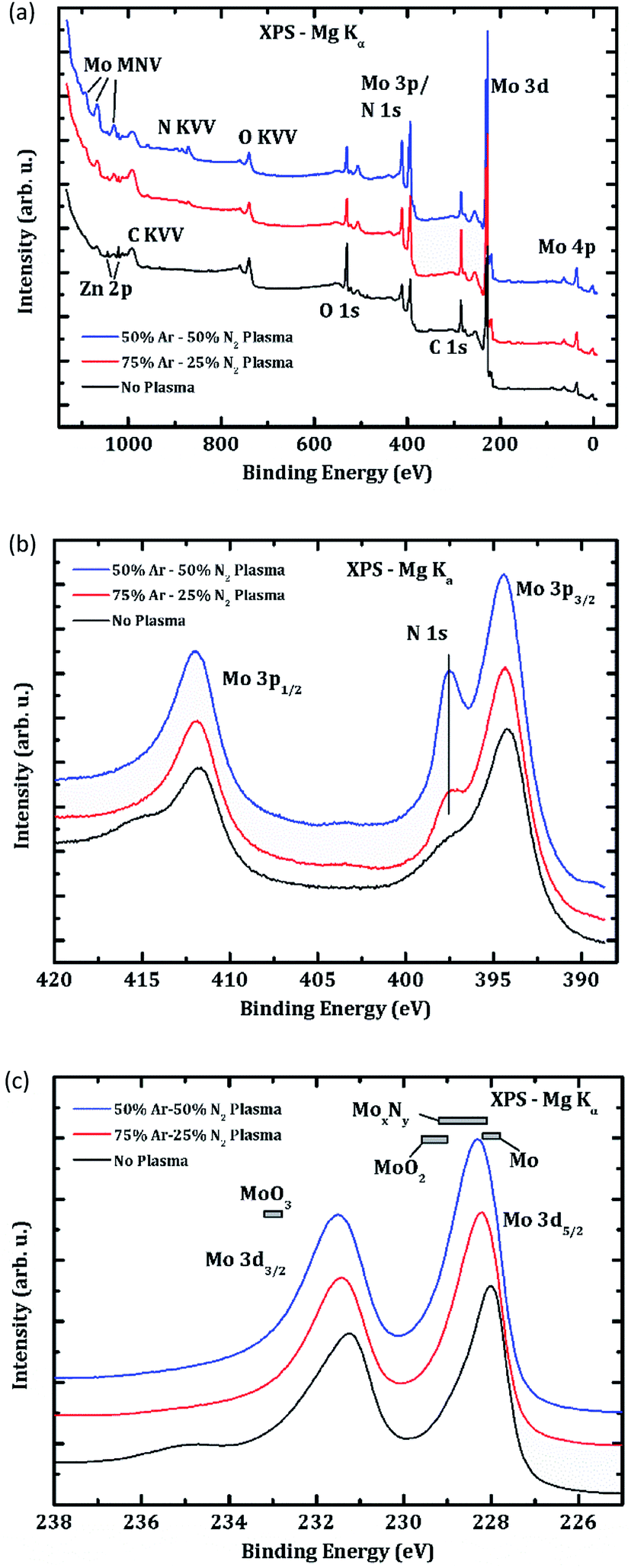 | ||
| Fig. 5 (a) XPS survey spectra, (b) Mo 3p and N 1s spectrum, and (c) Mo 3d spectrum of Mo substrates. Black spectra were recorded for a sample without Ar–N2 plasma treatment, red and blue spectra were collected after an Ar–N2 plasma treatment with an Ar/N ratio of 75/25 and 50/50, respectively. | ||
For both plasma-treated samples, clear N Auger-signals (N KVV ∼ 880 eV) are found, being more pronounced for the enhanced plasma treatment procedure. Furthermore, Fig. 5(b) shows a pronounced N 1s signal at 397.5 eV, which matches reported values for molybdenum nitrides.21 Fig. 5(b) also shows the Mo 3p1/2 and 3p3/2 peaks, which shift to higher binding energy after plasma treatment. Without the plasma treatment, a shoulder of the Mo peaks (at 398 eV for Mo 3p3/2 and 415 eV for Mo 3p1/2) is indicative of the presence of Mo oxide. Finally, Fig. 5(b) shows a small peak at ∼403 eV for both plasma-treated samples, which we ascribe to either embedded N2 and/or N–O bonds.21
Fig. 5(c) shows the Mo 3d signals, together with tabulated peak positions for the Mo 3d5/2 peak.21 The here observed position of the “no plasma” sample fits well with metallic Mo (and also shows a characteristic metallic asymmetry), while a shoulder best seen for the Mo 3d3/2 peak (at 235 eV) indicates the presence of Mo oxide. The Mo 3d peaks also shift towards higher binding energy for the plasma-treated samples (as expected), matching the tabulated values for MoxNy. To summarize the XPS results, we find a removal of Mo oxides, the formation of a MoxNy phase at the surface, and a small contribution of molecular N2 or N–O bonds after the Ar–N2 plasma treatments.
To analyze the impact of the different treatments on resulting device performance, solar cells were fabricated from untreated, Ar treated, and “standard mixed” plasma treated Mo substrates. The obtained efficiencies all ended up in the range of the usual reproducibility of our process and varied between 9.5% and 11.5% device efficiency, with no obvious trends. The results are shown and discussed in the ESI,† indicating a possible improvement of the sample uniformity as a result of plasma treatments and thus supporting the discussion in the previous section.
Plasma treatments with TiN back-contact barrier
The application of a TiN barrier layer on Mo back contacts was shown in literature in context of other CZTSSe fabrication methods to allow an effective reduction of MoSe2 formation.15,16 To investigate the impact of the Ar plasma treatment on the samples containing such a Se diffusion barrier layer and to obtain further insights into the impact of the overall MoSe2 thickness on the final solar cell performance, samples with a TiN back-contact barrier were also analyzed. In Fig. 6(a) and (b), SEM cross sections show a strongly reduced MoSe2 formation (MoSe2 thickness < 100 nm) for Mo/TiN back contacts, without and with Ar plasma treatment. For another sample containing a thin Mo layer on top of the Mo/TiN back contact (i.e., Mo/TiN/Mo back-contact arrangement), only the Mo atoms located above the TiN undergo selenization and form MoSe2 (thickness constant at ≈230 nm) (Fig. 6(c)). These results indicate that TiN works as an effective Se diffusion barrier also in our fabrication method, and that its effect is not reduced by the applied plasma treatment. | ||
| Fig. 6 SEM cross-section of CZTSe solar cells with TiN back-contact barriers: (a) Mo/TiN back contact without plasma treatment, (b) Mo/TiN back contact with Ar plasma treatment and (c) Mo/TiN/Mo back contact with Ar plasma treatment. | ||
Fig. 7 shows a comparison of the CZTSe solar cell performance with TiN back-contact barriers. In agreement with the previously reported work by Schnabel et al.16 on a solution-based fabrication process, the Mo/TiN/Mo back-contact structure shows superior behavior compared to the two cells with Mo/TiN back-contact configuration. The results suggest that the direct contact of TiN with the absorber layer has a negative impact on the back-interface properties, which may result from the existence of a potential electronic barrier induced by TiN between the CZTSe absorber and the Mo back contact. For the Mo/TiN/Mo case, in which no direct contact of TiN with the CZTSe absorber exists, the negative impact of TiN is largely eliminated, and the resulting CZTSe/MoSe2 interface may lead to improved electronic properties.2,13 The solar cells based on this configuration perform more closely (i.e., mainly 8–9% efficiency) to the devices without an extra back-contact barrier discussed above. However, the results do not indicate any improvement of the device properties for reducing the MoSe2 layer thickness from ≈1 μm range down to less than 250 nm.
 | ||
| Fig. 7 Box plots of solar cell parameters (a) energy conversion efficiency η, (b) open circuit voltage Voc, (c) short circuit current density Jsc and (d) fill factor FF for the samples with TiN back contact barriers. For every type of back contacts, 6 cells are included. | ||
Conclusions
To develop a reliable fabrication process for CZTSe-based thin-film solar cells with efficiencies >10%, stable back-contact interfaces with a reproducible and uniform behavior are important. This becomes even more critical for upscaling in an industrial context. An Ar plasma treatment of the Mo back contact before the deposition of the CZTSe absorber can significantly improve the morphological homogeneity and thickness uniformity at the back interface. However, it also facilitates the formation of a slightly thicker MoSe2 interfacial layer between the CZTSe absorber and the Mo back contact. A modified plasma treatment with a mixed Ar–N2 plasma was tested for further modification of the Mo back contact. By an appropriate adjustment of the parameters for the plasma process, a nitridation of the Mo surface (i.e., the formation of MoxNy compounds) is possible. This procedure provides a combination of the cleaning effect under Ar plasma with the formation of a very thin MoxNy layer that may act as a passivation layer at the back interface and lead to a reduction of MoSe2 formation during the selenization.For CZTSe based thin film solar cells, MoSe2 appears to play a beneficial role, in terms of adhesion and band alignment between the Mo back contact and the CZTSe absorber. Unless it is too thick or too inhomogeneous in thickness to cause mechanical instability, the thickness of MoSe2 does not seem to play a crucial role for the solar cell performance. In other words, as Mo still appears to be the best choice for back contacts of CZTSe solar cells, the focus of back-contact engineering in future research should be directed away from the general thickness concern and rather towards the understanding and improvement of more decisive properties of the formed MoSe2 layer and its interface to the absorber. This may include the as-grown crystalline direction and texture, as well as the optimal energy level alignment for a heterojunction with a low hole barrier and, possibly, an electron reflector at the back contact.
Conflicts of interest
There are no conflicts to declare.Acknowledgements
We gratefully acknowledge funding from the German Federal Ministry of Education and Research (BMBF), Free-InCa Project (grants 03SF0530A, 03SF0530B, and 03SF0530C), and the Deutsche Forschungsgemeinschaft (DFG, INST 121384/64-1 FUGG).Notes and references
- T. Wada, N. Kohara, S. Nishiwaki and T. Negami, Thin Solid Films, 2001, 387, 118–122 CrossRef CAS
.
- K. H. Ong, R. Agileswari, B. Maniscalco, P. Arnou, C. C. Kumar, J. W. Bowers and M. B. Marsadek, Int. J. Photoenergy, 2018, 2018, 9106269 CrossRef
- L. Weinhardt, O. Fuchs, A. Peter and E. Umbach, J. Chem. Phys., 2016, 124, 074705 CrossRef PubMed
- L. Weinhardt, M. Blum, M. Bär, C. Heske, O. Fuchs, E. Umbach, J. D. Denlinger, K. Ramanathan and R. Noufi, Thin Solid Films, 2007, 515, 6119–6122 CrossRef CAS
- M. Bär, S. Nishiwaki, L. Weinhardt, S. Pookpanratana, W. N. Shafarman and C. Heske, Appl. Phys. Lett., 2008, 93, 042110 CrossRef
- M. Bär, L. Weinhardt and C. Heske, Phys. Rev. B: Condens. Matter Mater. Phys., 2008, 78, 075404 CrossRef
- S. Oueslati, G. Brammertz, M. Buffière, H. ElAnzeery, D. Mangin, O. ElDalf, O. Touayar, C. Köble, M. Meuris and J. Poortmans, J. Phys. D: Appl. Phys., 2015, 48, 035103 CrossRef
- P. D. Antunez, D. M. Bishop, Y. S. Lee, T. Gokmen, O. Gunawan, T. S. Gershon, T. K. Todorov, S. Singh and R. Haight, Adv. Energy Mater., 2017, 7, 1602585 CrossRef
- G. Brammertz, M. Buffière, S. Oueslati, H. ElAnzeery, K. Ben Messaoud, S. Sahayaraj, C. Köble, M. Meuris and J. Poortmans, Appl. Phys. Lett., 2013, 103, 163904 CrossRef
- Y. S. Lee, T. Gershon, O. Gunawan, T. K. Todorov, T. Gokmen, Y. Virgus and S. Guha, Adv. Energy Mater., 2014, 2014, 1401372 Search PubMed
- T. Taskesen, J. Neerken, J. Schoneberg, D. Pareek, V. Steininger, J. Parisi and L. Gütay, Adv. Energy Mater., 2018, 8, 1703295 CrossRef
- A. Shigemi and T. Wada, Jpn. J. Appl. Phys., 2018, 57, 08RC17 CrossRef
- D. Cozza, C. M. Ruiz, D. Duché, J. J. Simon and L. Escoubas, IEEE J. Photovolt., 2016, 6, 5 Search PubMed
- J. Li, Y. Zhang, W. Zhao, D. Nam, H. Cheong, L. Wu, Z. Zhou and Y. Sun, Adv. Energy Mater., 2015, 5, 1402178 CrossRef
- B. Shin, Y. Zhu, N. A. Bojarczuk, S. Jay Chey and S. Guha, Appl. Phys. Lett., 2012, 101, 053903 CrossRef
- T. Schnabel and E. Ahlswede, Sol. Energy Mater. Sol. Cells, 2017, 159, 290–295 CrossRef CAS
- S. López-Marino, M. Placidi, A. Pérez-Tomás, J. Llobet, V. Izquierdo-Roca, X. Fontané, A. Fairbrother, M. Espíndola-Rodríguez, D. Sylla, A. Pérez-Rodríguez and E. Saucedo, J. Mater. Chem. A, 2013, 1, 8338–8343 RSC
- M. H. Sayed, J. Schoneberg, J. Parisi and L. Gütay, RSC Adv., 2017, 7, 20406–20411 RSC
- T. Taskesen, V. Steininger, W. Chen, J. Ohland, U. Mikolajczak, D. Pareek, J. Parisi and L. Gütay, Prog. Photovolt. Res. Appl., 2018, 26, 1003–1006 CrossRef CAS
- S. Uličná, P. Arnou, A. Abbas, M. Togay, L. M. Welch, M. Bliss, A. V. Malkov, J. M. Walls and J. W. Bowers, J. Mater. Chem. A, 2019, 7, 7042–7052 RSC
- NIST X-ray Photoelectron Spectroscopy Database, NIST Standard Reference Database Number 20, National Institute of Standards and Technology, Gaithersburg MD, 2000, p. 20899, http://srdata.nist.gov/xps/citation.aspx Search PubMed.
Footnote |
| † Electronic supplementary information (ESI) available. See DOI: 10.1039/c9ra02847a |
| This journal is © The Royal Society of Chemistry 2019 |