DOI:
10.1039/C9RA02669J
(Paper)
RSC Adv., 2019,
9, 18420-18428
Cu2ZnSn(S,Se)4 thin-films prepared from selenized nanocrystals ink
Received
9th April 2019
, Accepted 3rd June 2019
First published on 11th June 2019
Abstract
For the first time, CZTS ink was formulated using low-temperature heating up synthesis of NCs. Besides, the influence of powder concentration on the properties of the films was examined. Subsequently, the CZTS films were annealed under a selenium (Se)/argon (Ar) atmosphere at different temperatures to enhance their properties. The influence of selenization temperature on the properties of CZTS films was examined in detail. Structural analysis showed a peak shift towards lower 2θ values for CZTSSe films because of Se incorporation, resulting in larger lattice parameters for CZTSSe than CZTS. As the selenization temperature increases, an increment in the grain size was observed and the band gap was decreased from 1.52 to 1.05 eV. Hall Effect studies revealed a significant improvement in the mobility and carrier concentration with respect to selenization temperatures. Moreover, film selenized at 550 °C exhibited higher photoconductivity as compared to other films, indicating their potential application in the field of low-cost thin-film solar cells.
Introduction
Over the past few years, thin-film solar cells (TFSCs) fabricated from low-cost, earth-abundant and non-lethal elements have attracted remarkable research interest around the world. In this regard, Cu2ZnSn(S,Se)4 (CZTSSe) thin-films have emerged as a potential absorber layer in TFSCs due to their high absorption coefficient of over 104 cm−1, direct band gap and, most importantly, tunable band gap from 1 to 1.5 eV by varying the S/Se ratio.1–5 Mostly, various vacuum methods, such as sputtering,6,7 pulsed laser deposition8,9 and thermal evaporation10 have been extensively employed for the deposition of CZTS thin-films. However, vacuum methods require an expensive and complex operation to fabricate solar cells, which has always been an impediment for commercialization.11 On the other hand, solution-based approaches like nanocrystals (NCs) ink,12,13 electro-deposition14 and hydrazine-based ink15 have been widely used to produce low-cost and large area TFSCs. The highest power conversion efficiency (12.6%) of CZTSSe TFSCs have been reported using a hydrazine-based approach16 which is very harmful to researchers and the environment. Therefore, the NCs ink approach has greatly gained the researchers' attention, because it could be coated as thin-films using knife-coating, spin coating, printing and spraying methods under ambient conditions.17–19 Moreover, C. K. Miskin et al.20 reported the highest power conversion efficiency (PCE) of CZTS NCs based solar cells as high as 9.0%, in which they used a hot-injection method to synthesize NCs. However, hot-injection synthesis is not appropriate for scaling-up process due to its difficulty in controlling the monomer release.21 To overcome these drawbacks, researchers have recently instigated the heating up synthesis of CZTS NCs,22,23 but they used expensive materials, multi-solvents and high reaction temperature > 250 °C, which is not suitable for the industrial applications. Therefore, it is necessary to develop a simple and low-cost synthesis method for CZTS NCs to fabricate and commercialize thin film solar cell devices. In this concern, we have synthesized the uniform CZTS NCs at low-temperature using simplistic and less expensive materials.24 Besides, the coating of these NCs as thin-films is an essential part for the solar cell applications and there is no report in the literature for the coating of NCs synthesized by heating up approach. Moreover, fabrication of thin-films with uniform thickness, densely packed grains and crack-free surface are considered to be a crucial part in case of NCs ink approach.
To the best of our knowledge, this is the first report which deals with the preparation of CZTS films using NCs synthesized by low-temperature heating up process. Herein, we have formulated NCs inks which are highly stable, possessing homogeneous size distribution and shape-controlled characteristics that helps to attain the uniform coatings with compact grains while depositing thin-films using knife-coating. Subsequently, the films were subjected to air annealing at 350 °C for 1 min to evaporate the solvent. In addition, the crack-free thin-films were obtained by varying the CZTS NCs concentration. Selenization process was carried out for the annealed films to replace the majority of sulfur (S) atoms with Se atoms. Furthermore, the selenization temperatures were varied to study their influences on the properties of CZTS films. As the selenization temperature increases, a significant improvement in the optical, electrical and optoelectronic properties was observed. Hence, this work could provide a new avenue to prepare CZTS thin-films by a cost-effective approach, which is suitable for large scale production and roll-to-roll TFSCs fabrication process.
Experimental procedure
CZTS thin-film preparation and pre-annealing
As described in the previous section, the synthesized CZTS NCs were used to deposit thin-films. The ink was formulated by dispersing NCs in hexanethiol solvent and sonicated for 60 min. To obtain crack-free thin-films, the powder concentration was varied such as 0.05, 0.1 and 0.2 g in 1 mL hexanethiol. Then, the ink was spread over soda-lime glass substrates by knife-coating. A layer of scotch tape was used as the spacer for thin-film preparation. Two alternative coatings were applied to ensure uniform film thickness. After each coating, the film was annealed at 350 °C for 1 min in the pre-heated oven to evaporate the solvent and carbon.
Selenization of CZTS thin-films
CZTS thin-films were annealed under Se/Ar atmosphere. 50 mg of Se and 5 mg of tin (to avoid the tin loss) powder were placed into the graphite box along with CZTS film and kept inside the furnace. A two-step selenization was carried out using a partially closed graphite box under Ar atmosphere. In the first step, the film was annealed at 400 °C for 30 min to incorporate the Se into CZTS crystal lattice. During the second step, the temperature was further increased to 500 °C for 15 min to facilitate the recrystallization and enhance grain growth. The ramp of temperature was 20 °C min−1. The selenization temperature in the second step was varied such as 500, 525 and 550 °C by keeping a constant time of 15 min.
Characterization
Structural properties of CZTS and CZTSSe thin-films were obtained using X-ray diffractometer (XRD, PANanalytical) and Raman (HORIBA Jobin Yvon) spectrometer. Field emission scanning electron microscopy (FE-SEM-Auriga 3916, Carl Zeiss) and energy dispersive analysis of X-ray spectroscopy (EDAX) were employed to measure the morphology and composition of the samples. The optical measurements were carried out using ultraviolet-visible-near-infrared (UV-Vis-NIR) spectrophotometer (JASCO V-670). The electrical properties of films were measured using a Hall-effect measurement. The current–voltage curve (I–V) of CZTS and CZTSSe thin-films were collected with standard I–V measurement equipment of Keithley 4200-SCS. The I–V measurements were performed in dark and under the illumination of light with the intensity of 9.45 mW cm−2 using tungsten lamp (Philips).
Results and discussions
As-deposited thin-films
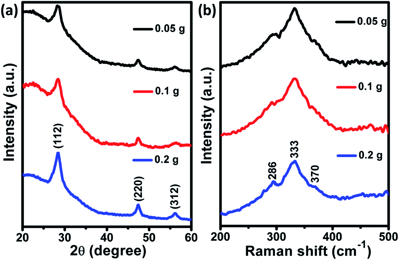
XRD patterns of as-deposited CZTS films for different powder concentrations are shown in Fig. 1(a). The observed (112), (220) and (312) planes were similar to the powder samples which can be seen from our previously published article.24 It indicates that crystalline properties of CZTS powder were unaffected during the process of film fabrication. Besides, the diffraction peak intensity was reduced as the powder concentration decreases, which could be due to the reduction of film thickness. Raman spectra (Fig. 1(b)) displayed a major peak at 333 cm−1, corresponding to A1 mode of kesterite CZTS. Besides, two shoulder peaks were observed at 286 and 370 cm−1, attributed to kesterite CZTS.25,26
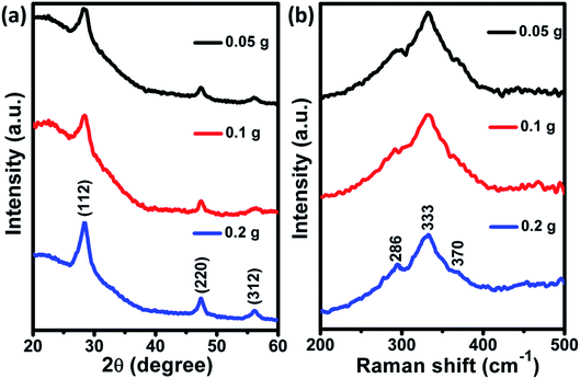 |
| | Fig. 1 (a) XRD pattern and (b) Raman spectra of as-deposited CZTS films at different powder concentration. | |
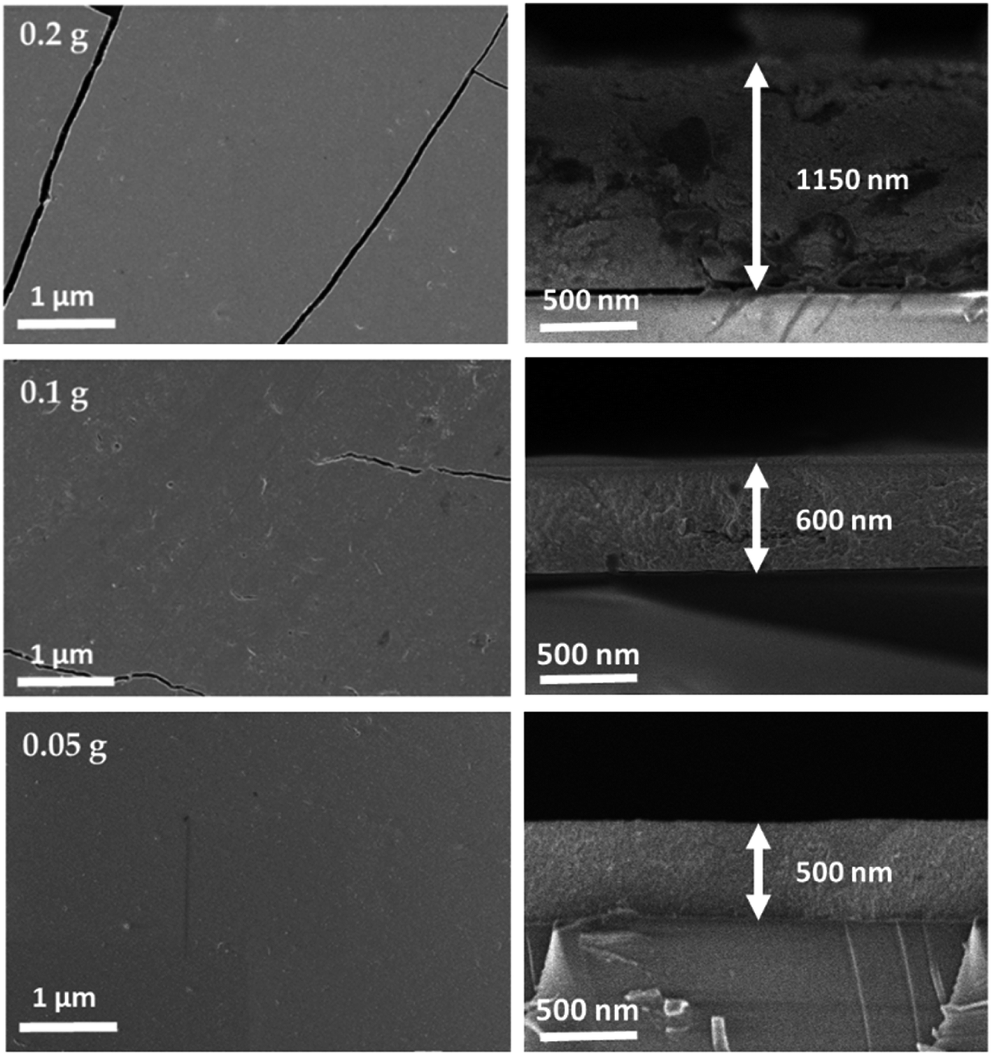
Fig. 2 depicts the planar and cross-sectional morphology of as-deposited CZTS films for different powder concentration. Both planar and cross-sectional FE-SEM images showed the crack free and smooth surface for all the samples. From the cross-sectional images, the observed thickness of as-deposited films is 1200, 700 and 600 nm for 0.2, 0.1 and 0.05 g of powder concentration respectively. Thus, the results revealed that the thickness of films was directly proportional to the powder concentration. EDAX compositional analysis of as-deposited CZTS films is shown in Table 1. The observed elemental composition is close to the powder concentration.24 Besides, slight increment in the S content was observed because of the solvent (hexanethiol) used for the ink preparation.
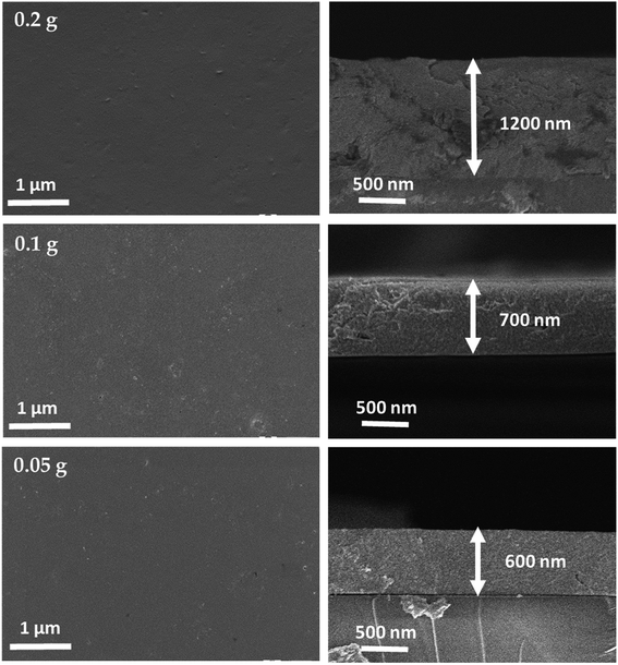 |
| | Fig. 2 Planar and cross-sectional FE-SEM images of as-deposited CZTS films at different powder concentration. | |
Table 1 EDAX composition of as-deposited CZTS films at different powder concentration
| Powder concentration (g) |
Elemental composition (atomic%) |
Composition ratio |
| Cu |
Zn |
Sn |
S |
C |
Cu/(Zn + Sn) |
Zn/Sn |
| 0.2 |
21.81 |
13.67 |
12.22 |
52.30 |
48.10 |
0.84 |
1.12 |
| 0.1 |
21.19 |
14.29 |
12.35 |
52.17 |
46.16 |
0.80 |
1.15 |
| 0.05 |
21.70 |
14.16 |
12.30 |
51.84 |
45.50 |
0.82 |
1.15 |
Air annealing of CZTS thin-films
Planar and cross-sectional FE-SEM images of CZTS films annealed at 350 °C are shown in Fig. 3. As can be seen from Fig. 3, cracks were observed for the films prepared at the powder concentration of 0.2 and 0.1 g. Formation of these cracks could be due to differences in the thermal expansion (or shrinkage) between the glass substrate and the CZTS. Besides, film thickness, binder removal, solvent evaporation rate, annealing temperature and time plays a vital role in the formation of cracks.27,28 These cracks should be avoided as it can create a shunt path in the absorber thereby affecting the solar cell performance. When the CZTS film annealed at 350 °C, ligand molecules desorb and/or thermally decomposes into volatile species, which is responsible for the reduction of both sulfur and carbon content (Table 2). Hence, the evaporation of solvent resulting volume shrinkage in the film which leads to stress that induces cracks during annealing. Besides, the cracks were reduced as the film thickness decreased from 1150 to 500 nm, which could be due to decrement in the volume shrinkage that reduces the stress as well. Finally, a crack-free film with a uniform thickness of 500 nm was obtained for 0.05 g of powder concentration. EDAX composition analysis of CZTS films annealed at 350 °C is shown in Table 2. The film showed a similar composition to the powder samples. Both the sulfur and carbon contents were reduced as compared to the as-deposited films (Table 1).
 |
| | Fig. 3 Planar and cross-sectional FE-SEM images of CZTS films annealed at 350 °C for different powder concentration. | |
Table 2 EDAX composition of annealed CZTS films at different powder concentration
| Powder concentration (g) |
Elemental composition (atomic%) |
Composition ratio |
| Cu |
Zn |
Sn |
S |
C |
Cu/(Zn + Sn) |
Zn/Sn |
| 0.2 |
21.98 |
14.22 |
12.25 |
51.56 |
44.76 |
0.83 |
1.16 |
| 0.1 |
22.06 |
14.37 |
12.23 |
51.33 |
42.06 |
0.82 |
1.17 |
| 0.05 |
21.96 |
14.68 |
12.43 |
50.93 |
41.76 |
0.81 |
1.18 |
Selenization of CZTS thin-films
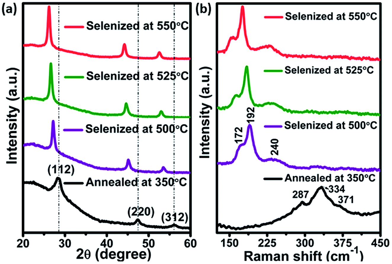
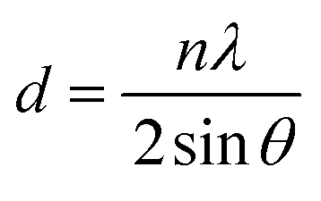
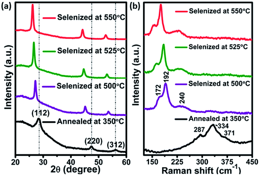
Films annealed at 350 °C with powder concentration of 0.05 g were further used for selenization. Fig. 4(a), showed the XRD patterns of annealed and selenized CZTS films. The annealed film showed the diffraction peaks at 2θ values of 28.45, 47.60 and 56.10°, corresponding to (112), (220) and (312) planes of kesterite CZTS. After selenization, the peaks were shifted to lower 2θ values for all the cases. The same behavior was observed by other researchers.29,30 The peak shift is due to the replacement of the majority of smaller sized S atoms (0.184 nm) by larger sized Se (0.198 nm) atoms during the selenization process, resulting in larger lattice parameters for CZTSSe than CZTS. The lattice parameters a and c were calculated from the XRD data of the annealed and selenized film at 550 °C, using the following formula:| |
 | (1) |
where h, k and l are Miller indices, a and c are lattice constants and d is the inter-planar distance.
 |
| | Fig. 4 (a) XRD pattern and (b) Raman spectra of annealed and selenized films at different temperature. | |
The inter-planar distance was estimated by using Bragg's diffraction equation:
| |
 | (2) |
where
n is a positive integer,
λ is wavelength (1.5405 Å) and
θ is Bragg's angle.
The calculated lattice parameters a and c values for CZTS film are 5.42 and 10.85 Å respectively but for the CZTSSe film, the a and c were shifted to 5.63 and 11.30 Å respectively, which is in good accordance with the literature.30,31 To further confirm the phase purity, Raman measurements were carried out for the annealed and selenized films. As can be seen in Fig. 4(b), Raman peaks were observed at 334, 287 and 371 cm−1 for annealed films. The film selenized at 500 °C showed the A1 mode shift of CZTSe at around 172, 192 and 240 cm−1 32,33. The peak position of the A1 mode was shifted further, as the selenization temperature increases. Most importantly, no secondary phases like Cu2S, ZnS, ZnSe, CTS etc., were observed which confirms the pure phase formation of CZTSSe.
FE-SEM images of CZTS films selenized at different temperature are shown in Fig. 5. Film selenized at 500 °C showed a few voids on the surface, which could be due to insufficient Se incorporation as can be observed from the EDAX analysis (Fig. 6(a)). When the selenization temperature increased to 525 °C, voids were reduced significantly. Further increasing the temperature to 550 °C, results in void-free, smooth surface and compact morphology of CZTSSe, which is due to more Se incorporation into the films. It is interesting to note that the thickness of CZTSSe films was increased from 500 to 800 nm as compared to annealed film, which could be due to volume expansion in the unit cell when the Se is incorporated into the lattice as mentioned in the XRD analysis.
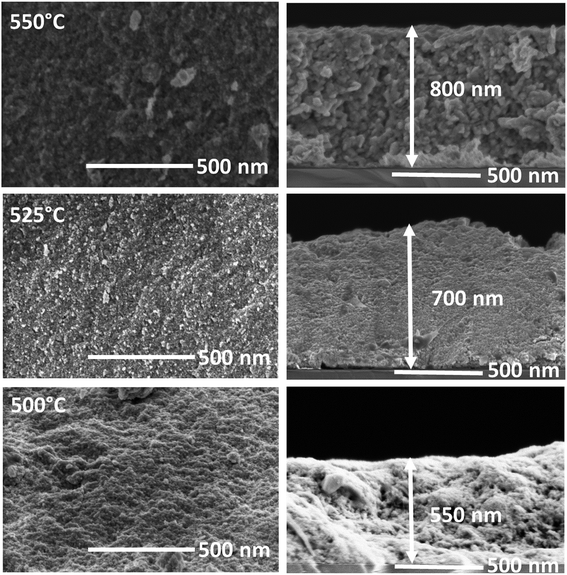 |
| | Fig. 5 Planar and cross-sectional FE-SEM images of CZTSSe films at different selenization temperature. | |
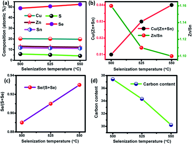 |
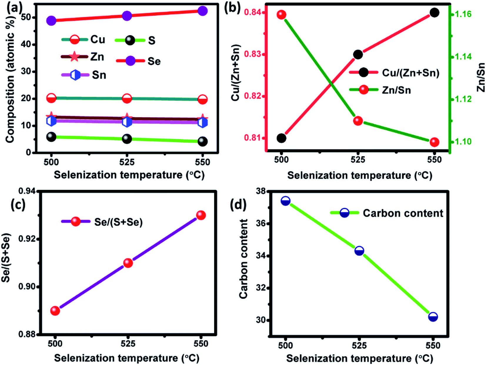
| | Fig. 6 (a) The elemental composition, (b) the corresponding ratio of Cu/(Zn + Sn) and Zn/Sn, (c) Se/(S + Se) ratio and (d) carbon content of the films selenized at different temperature. | |
EDAX compositional analysis was performed for the films selenized at different temperature. The elemental composition varied with increases in the selenization temperature as shown in Fig. 6(a). The Cu/(Zn + Sn) ratio increases while the Zn/Sn ratio decreases as a function of selenization temperature (Fig. 6(b)). With increases in the selenization temperature, Se/(S + Se) ratio increases as the amount of S decreases which can be observed from Fig. 6(c). Furthermore, the carbon content was reduced as the selenization temperature increases (Fig. 6(d)). The selenized films showed Cu-poor, Zn-rich composition, which is considered to be an optimum condition for highly efficient TFSCs.34
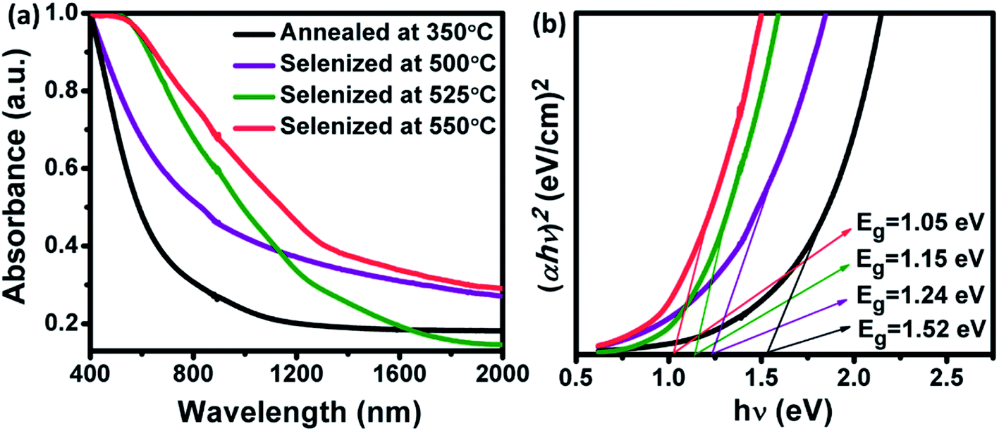
UV-Vis-NIR absorbance measurements were performed for the annealed and selenized films at different temperature. The absorbance spectra and the corresponding band gap of the samples are shown in Fig. 7. The optical band gap was calculated using the following formula
where,
α is the absorption coefficient,
hν is photon energy,
A is a constant.
35 The optical band gap was achieved by plotting (
αhν)
2 as a function of
hν. The calculated band gap energy for the annealed film is 1.52 eV, which is in good accordance with the powder sample.
24 However, the band gap energy was systematically decreased to 1.05 eV for CZTSSe films with an increment in the Se/(S + Se) ratio (
Fig. 7(b)). The observed band gap values were consistent with the reported values.
36,37 Moreover, the narrow band gap energy could help to improve the efficiency of CZTSSe TFSCs.
38
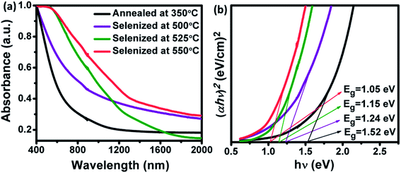 |
| | Fig. 7 (a) UV-Vis-NIR absorption spectra and (b) corresponding band gap of annealed and selenized CZTS films at different selenization temperatures. | |
The conductivity type, carrier concentration, mobility and resistivity of both CZTS and CZTSSe films were measured by Hall-effect. The reported value of mobility and carrier concentration for CZTS absorber material is in the range of 1 to 10 cm2 V−1 s−1 and 1016 to 1018 cm−3.39,40 As can be seen in Table 3, all the films showed p-type conductivity. CZTS film showed higher resistivity and lower mobility of charge carriers because it consists of smaller grains as can be observed from the FE-SEM images, which leads to the high density of grain boundaries that hinders the flow of charge carriers. For CZTSSe films, carrier concentration and mobility were inversely proportional to the resistivity. As the selenization temperature increases, mobility increased further which could be due to the improvement in both the crystallite and grain size41 as observed from XRD, Raman and FE-SEM analyses. Therefore, the film selenized at 550 °C showed higher mobility and less resistivity when compared to other films which reveal that the obtained CZTSSe film is suitable for solar cell applications.
Table 3 Carrier type, carrier concentration, mobility, and resistivity of annealed and selenized films at different temperature
| Experimental conditions |
Type of conductivity |
Carrier concentration (cm−3) |
Mobility (cm2 V−1 s−1) |
Resistivity (Ωcm) |
| Annealed at 350 °C |
p |
1.13 × 10¹⁶ |
0.05 |
1.70 |
| Selenized at 500 °C |
p |
2.17 × 10¹⁷ |
0.80 |
1.23 |
| Selenized at 525 °C |
p |
4.32 × 10¹⁷ |
1.92 |
0.41 |
| Selenized at 550 °C |
p |
7.52 × 10¹⁷ |
3.14 |
0.21 |
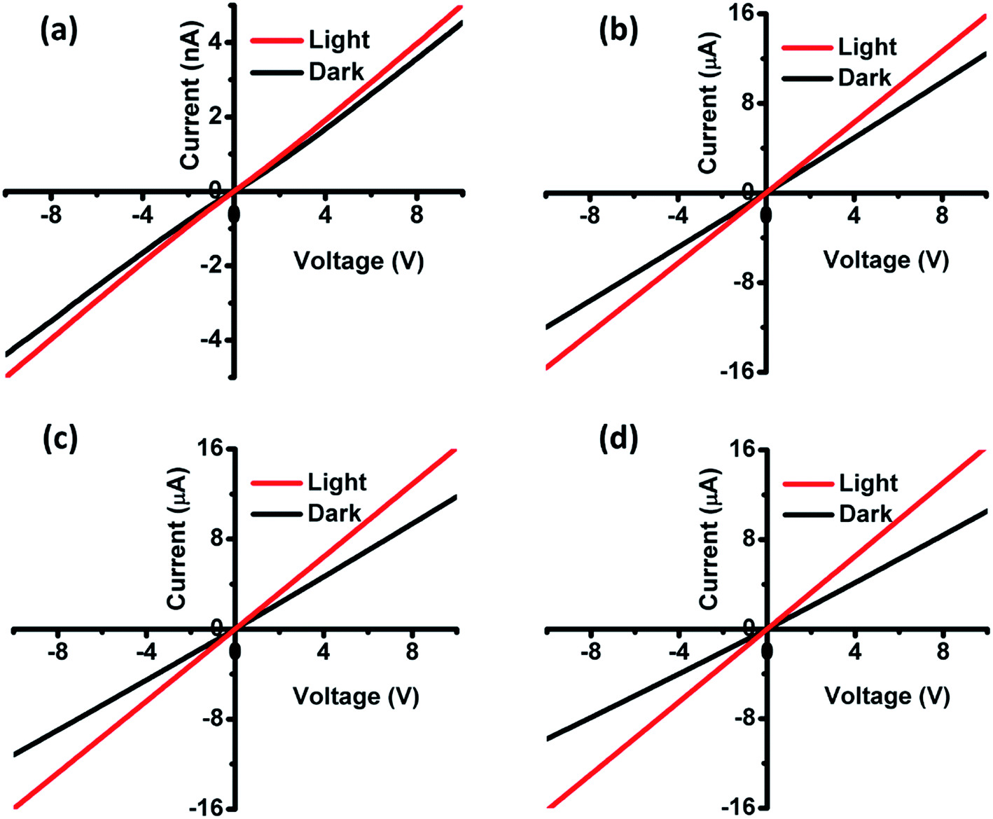
To perform the I–V measurements, gold (Au) circular contacts with a thickness of 200 nm were deposited onto the film using thermal evaporation. The I–V measurements were carried out between the two Au contacts at a given bias voltage of 10 V. From the Fig. 8, we could observe a linear I–V curve, which implies that the metal (Au) contacts are ohmic in nature.42–44 The photo-response properties of CZTS and CZTSSe films were measured in dark and under the illumination of light. The illumination helps to excite the electrons from the valence band to the conduction band which obviously enhances the holes in the CZTS and CZTSSe that enhances the conductivity of the films. The photoconductivity of films can be expressed by ΔI (the current difference between the dark and under the illumination of light). The photocurrent ΔI is calculated by Iphoton/Idark in CZTS and CZTSSe thin-films were 1.09 nA, 1.27 μA, 1.35 μA and 1.65 μA cm−2, respectively. The film selenized at 550 °C showed higher photoconductivity as compared to other films, suggesting their potential applications in the field of TFSCs.
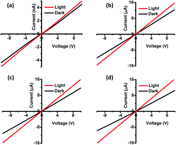 |
| | Fig. 8 Dark and light I–V characteristics of films (a) annealed at 350 °C, (b) selenized at 500 °C, (c) selenized at 525 °C and (d) selenized at 550 °C. | |
Conclusions
CZTS ink was formulated using the NCs synthesized by low-temperature heating up approach. Subsequently, the ink was coated as thin-films using knife-coating followed by annealing. The annealed CZTS films exhibited similar structural, morphological and compositional properties to the powder. Then, the films were annealed under Se/Ar atmosphere at different temperature to enhance the film properties. Structural analysis showed a peak shift towards lower wavelength for CZTSSe films due to Se incorporation into the film. The band gap was tuned from 1.52 to 1.05 eV as a function of selenization temperature. From the morphological analysis, a void-free and smooth surface was observed for the film selenized at 550 °C. Compositional analysis revealed the Cu-poor, Zn-rich composition which is the optimum condition for highly efficient CZTS TFSCs. As the selenization temperature increases, improvement in the mobility and carrier concentration were observed from the Hall effect measurements. Furthermore, film selenized at 550 °C showed higher photoconductivity as compared to other films. Therefore, the results suggested that the obtained CZTSSe film can be employed as an absorber layer in low-cost TFSCs.
Conflicts of interest
There are no conflicts to declare.
Acknowledgements
Authors acknowledge the CeMIE-Sol, P-55 project for their financial support and Dr R. Aruna-Devi acknowledges the postdoctoral fellowship from Fondo Sectorial CONACYT-Secretarìa de Energìa-Sustentabilidad Energètica 2018-2019. We thank Adolfo Tavira (XRD), Miguel Galván Arellano (Raman and I–V characteristics), Jorge Roque de la Puente (LANE-Cinvestav) for FE-SEM and EDAX analysis, Miguel Ángel Luna Arias (Hall Effect measurement) and Angela Gabriela Lopez Fabian (UV-Vis NIR analysis) for their characterization help.
References
- S. W. Shin, W. R. Bae, H. S. Yang, C. W. Hong, H. R. Jung, M. P. Suryawanshi, K. V. Gurav, S. M. Pawar, P. S. Patil, J. Y. Lee and J. H. Kim, RSC Adv., 2014, 4, 32530–32533 RSC.
- Y. Havryliuk, M. Y. Valakh, V. Dzhagan, O. Greshchuk, V. Yukhymchuk, A. Raevskaya, O. Stroyuk, O. Selyshchev, N. Gaponik and D. R. T. Zahn, RSC Adv., 2018, 8, 30736–30746 RSC.
- Y. Gao, H. Yang, Y. Zhang, J. Li, H. Zhao, J. Feng, J. Sun and Z. Zheng, RSC Adv., 2014, 4, 17667–17670 RSC.
- S. Chen, H. Tao, Y. Shen, L. Zhu, X. Zeng, J. Tao and T. Wang, RSC Adv., 2015, 5, 6682–6686 RSC.
- J. Wang, P. Zhang, X. Song and L. Gao, RSC Adv., 2015, 5, 1220–1226 RSC.
- J. Han, S. W. Shin, M. G. Gang, J. H. Kim and J. Y. Lee, Nanotechnology, 2013, 24, 095706 CrossRef PubMed.
- M. Banavoth, S. Dias and S. B. Krupanidhi, AIP Adv., 2013, 3, 082132 CrossRef.
- G.-X. Liang, Y.-D. Luo, J.-G. Hu, X.-Y. Chen, Y. Zeng, Z.-H. Su, J.-T. Luo and P. Fan, Surf. Coat. Technol., 2019, 358, 762–764 CrossRef CAS.
- A. V. Moholkar, S. S. Shinde, G. L. Agawane, S. H. Jo, K. Y. Rajpure, P. S. Patil, C. H. Bhosale and J. H. Kim, J. Alloys Compd., 2012, 544, 145–151 CrossRef CAS.
- C. Sripan, R. Ganesan, R. Naik and A. K. Viswanath, Opt. Mater., 2016, 62, 199–204 CrossRef CAS.
- T. K. Todorov, O. Gunawan, T. Gokmen and D. B. Mitzi, Prog. Photovoltaics, 2013, 21, 82–87 CAS.
- Y. Sun, H. Zheng, X. Li, K. Zong, H. Wang, J. Liu, H. Yan and K. Li, RSC Adv., 2013, 3, 22095–22101 RSC.
- B. Zhou, D. Xia and Y. Wang, RSC Adv., 2015, 5, 70117–70126 RSC.
- K. Cheng, Z. Kuang, J. Liu, X. Liu, R. Jin, Z. Lu, Y. Liu, L. Guo and Z. Du, J. Mater. Sci., 2017, 52, 11014–11024 CrossRef CAS.
- S. Bag, O. Gunawan, T. Gokmen, Y. Zhu, T. K. Todorov and D. B. Mitzi, Energy Environ. Sci., 2012, 5, 7060–7065 RSC.
- W. Wang, M. T. Winkler, O. Gunawan, T. Gokmen, T. K. Todorov, Y. Zhu and D. B. Mitzi, Adv. Energy Mater., 2014, 4, 1301465 CrossRef.
- J. Wang, P. Zhang, X. Song and L. Gao, RSC Adv., 2014, 4, 21318–21324 RSC.
- A. Irkhina, S. Levcenko, V. Hinrichs, P. Plate and T. Unold, RSC Adv., 2017, 7, 11752–11760 RSC.
- D. Vaccarello, A. Tapley and Z. Ding, RSC Adv., 2013, 3, 3512–3515 RSC.
- C. K. Miskin, W.-C. Yang, C. J. Hages, N. J. Carter, C. S. Joglekar, E. A. Stach and R. Agrawal, Prog. Photovoltaics, 2015, 23, 654–659 CAS.
- S. Engberg, Z. Li, J. Y. Lek, Y. M. Lam and J. Schou, RSC Adv., 2015, 5, 96593–96600 RSC.
- A. S. R. Chesman, N. W. Duffy, S. Peacock, L. Waddington, N. A. S. Webster and J. J. Jasieniak, RSC Adv., 2013, 3, 1017–1020 RSC.
- Y. Park, H. Jin, J. Park and S. Kim, CrystEngComm, 2014, 16, 8642–8645 RSC.
- R. Aruna-Devi, M. Latha, S. Velumani, J. Santoyo-salazar and J. Santos-cruz, Mater. Res. Bull., 2019, 111, 342–349 CrossRef CAS.
- R. Saravana Kumar, B. D. Ryu, S. Chandramohan, J. K. Seol, S.-K. Lee and C.-H. Hong, Mater. Lett., 2012, 86, 174–177 CrossRef CAS.
- V. T. Tiong, J. Bell and H. Wang, Beilstein J. Nanotechnol., 2014, 5, 438–446 CrossRef PubMed.
- G. C. A. M. Janssen, Thin Solid Films, 2007, 515, 6654–6664 CrossRef CAS.
- C. Liewhiran and S. Phanichphant, Sensors, 2007, 7, 650–675 CrossRef CAS.
- Z. Li, J. C. W. Ho, K. K. Lee, X. Zeng, T. Zhang, L. H. Wong and Y. M. Lam, RSC Adv., 2014, 4, 26888–26894 RSC.
- X. Zeng, K. F. Tai, T. Zhang, C. W. J. Ho, X. Chen, A. Huan, T. C. Sum and L. H. Wong, Sol. Energy Mater. Sol. Cells, 2014, 124, 55–60 CrossRef CAS.
- S. Das and K. C. Mandal, Mater. Res. Bull., 2014, 57, 135–139 CrossRef CAS.
- D. B. Khadka, S. Y. Kim and J. H. Kim, J. Phys. Chem. C, 2016, 120, 4251–4258 CrossRef CAS.
- J. Guo, Y. Pei, Z. Zhou, W. Zhou, D. Kou and S. Wu, Nanoscale Res. Lett., 2015, 10, 1045 Search PubMed.
- Q. Guo, G. M. Ford, W.-C. Yang, B. C. Walker, E. A. Stach, H. W. Hillhouse and R. Agrawal, J. Am. Chem. Soc., 2010, 132, 17384–17386 CrossRef CAS PubMed.
- N. M. Shinde, P. R. Deshmukh, S. V. Patil and C. D. Lokhande, Mater. Res. Bull., 2013, 48, 1760–1766 CrossRef CAS.
- X. Wang, Z. Sun, C. Shao, D. M. Boye and J. Zhao, Nanotechnology, 2011, 22, 245605 CrossRef PubMed.
- Y. Sun, Y. Zhang, H. Wang, M. Xie, K. Zong, H. Zheng, Y. Shu, J. Liu, H. Yan, M. Zhu and W. Lau, J. Mater. Chem. A, 2013, 1, 6880–6887 RSC.
- K. R. Choudhury, Y. Cao, J. V. Caspar, Q. Guo, L. K. Johnson, I. Malajovich, D. Radu, H. D. Rosenfeld, L. Silverman and W. Wu, IEEE Photovoltaic
Spec. Conf., 34th, 2013, 0043–0046 CAS.
- N. Muhunthan, O. P. Singh and V. N. Singh, Proc. SPIE, Micro/Nano Materials, Devices, and Systems, 2013, vol. 8923, p. 89232H Search PubMed.
- T. Tanaka, T. Nagatomo, D. Kawasaki, M. Nishio, Q. Guo, A. Wakahara, A. Yoshida and H. Ogawa, J. Phys. Chem. Solids, 2005, 66, 1978–1981 CrossRef CAS.
- K. C. Wang, P. Chen and C.-M. Tseng, CrystEngComm, 2013, 15, 9863–9868 RSC.
- S. Sarkar, K. Bhattacharjee, G. C. Das and K. K. Chattopadhyay, CrystEngComm, 2014, 16, 2634–2644 RSC.
- B. Ananthoju, A. Kushwaha, F. J. Sonia and M. Aslam, AIP Conf. Proc., 2013, 1512, 706–707 CrossRef CAS.
- M. Latha, R. Aruna Devi and S. Velumani, Opt. Mater., 2018, 79, 450–456 CrossRef CAS.
|
| This journal is © The Royal Society of Chemistry 2019 |
Click here to see how this site uses Cookies. View our privacy policy here. 
 Open Access Article
 This Open Access Article is licensed under a Creative Commons Attribution-Non Commercial 3.0 Unported Licence
 *a,
M. Latha
*a,
M. Latha