
 Open Access Article
 This Open Access Article is licensed under a Creative Commons Attribution-Non Commercial 3.0 Unported Licence
A novel synthesis of silver nanowires by using 6-chlorohexylzinc bromide as an additive for low haze transparent conductive films
Ximin Yuan,
Hongwei Yang *,
Yuxiu Li,
Yunxiu Chao,
Yao Li,
Li Chen and
Jialin Chen*
*,
Yuxiu Li,
Yunxiu Chao,
Yao Li,
Li Chen and
Jialin Chen*
State Key Laboratory of Advanced Technologies for Comprehensive Utilization of Platinum Metals, Kunming Institute of Precious Metals, 650106 Kunming, People's Republic of China. E-mail: nanolab@ipm.com.cn
First published on 17th June 2019
Abstract
High-quality silver nanowires (AgNWs) with a small diameter of ∼20 nm and a length of ∼40 μm were prepared by using a novel organic 6-chlorohexylzinc bromide as an assistant additive. The diameter of as-synthesized AgNWs was confirmed to be strongly dependent on the dosage of 6-chlorohexylzinc bromide. Moreover, a two-dimensional (2D) transparent conductive film (TCF) with an excellent optical performance was fabricated by as-synthesized AgNWs, which has a 90.3% transmittance and low haze value of <1.0% at a sheet resistance of 48.7 Ω sq−1.
1. Introduction
Currently, indium tin oxide (ITO), which is a transparent conductive material, widely used in highly transparent display devices, because it has relatively low resistivity. However, the ITO films are brittle and easily broken by an externally applied bending force, which have high brittleness and poor flexibility.1,2 With the development of technology and society, in order to meet people's needs for medicine,3 flexible touch screens,4 solar cells,5 wearable devices,6 etc., AgNWs are attracting much attention for their unique electronic conductivity and good flexibility. Therefore, it is very necessary to study and prepare high-quality AgNWs, making it become an ITO replacement material with realistic application prospects, especially as a popular material for flexible screen production.Thus far, there are many ways to prepare AgNWs, for example, electrochemical method,7 hydrothermal method,8 and microwave-assisted method,9 etc. Xi et al. successfully synthesized AgNWs with different diameters (28 nm, 38 nm, 55 nm, 80 nm) through direct-current electrochemical deposition technique, but needed to prepare the template in advance, and it also required complex post-processing.7 Xu et al. synthesized AgNWs with 30 nm in diameter by hydrothermal process in the presence of gemini surfactant; however, the operation was complex and needed two surfactants.8 Ying et al. synthesized AgNWs with the diameter of 40 nm through a microwave-assisted polyol reduction method using 1,2-ethanedithiol as both a reducing reagent and a solvent. But the length of AgNWs was as low as ∼2.2 μm.9 In contrast, AgNWs are mostly prepared by the polyol method. For example, You et al. prepared the AgNWs with diameter of 20 nm by reducing silver nitrate in ethanol solution with dodecylamine as a complex. But the reaction time was too long (heating at 100 °C for 24 h).10 Also, Silva et al. synthesized AgNWs with the diameter of 20 nm by using sodium bromide as a capping agent. However, the length of AgNWs synthesized only approached 20 μm.11 Lee et al. successfully prepared 15 nm AgNWs, which required two additives (NaCl and KBr) and high pressure conditions.12 Thus, it is still necessary to develop a facile method for synthesis of high-quality AgNWs.
In this study, organic 6-chlorohexylzinc bromide was first used to replace the traditional inorganic halide to prepare high-quality AgNWs. The probable controlled mechanism of 6-chlorohexylzinc bromide on the formation of AgNWs was discussed in details. Moreover, flexible transparent conductive films with low haze and resistance were thus fabricated based on the as-prepared AgNWs, indicating the potential application in flexible screen.
2. Experimental
2.1 Materials
Silver nitrate (AgNO3, ≥99.8%) was purchased from Sinopharm Chemical Reagent Co., Ltd. Ethylene glycol (EG, ≥99.0%), polyvinylpyrrolidone (PVP, Mw ∼ 1![[thin space (1/6-em)]](https://www.rsc.org/images/entities/char_2009.gif) 300000) were acquired from Sigma Aldrich. Ethanol (C2H5OH, ≥99.0%) was acquired from Xilong Chemical Co., Ltd. 6-Chlorohexylzinc bromide (6CHZB, 0.5 M in tetrahydrofuran, density of 0.89) was purchased from Fluorochem Ltd., and hydroxyethyl cellulose (HEC, QP-100 MH) was purchased from Dow. Deionized (DI) water was prepared by using a laboratory water purification system with a resistivity of not less than 18.2 MΩ cm and an operating temperature of 25 °C. All chemicals were used as received without further purification.
300000) were acquired from Sigma Aldrich. Ethanol (C2H5OH, ≥99.0%) was acquired from Xilong Chemical Co., Ltd. 6-Chlorohexylzinc bromide (6CHZB, 0.5 M in tetrahydrofuran, density of 0.89) was purchased from Fluorochem Ltd., and hydroxyethyl cellulose (HEC, QP-100 MH) was purchased from Dow. Deionized (DI) water was prepared by using a laboratory water purification system with a resistivity of not less than 18.2 MΩ cm and an operating temperature of 25 °C. All chemicals were used as received without further purification.
2.2 Methods
:1) by stirring at 25 °C for 3 h, and eventually the uniform AgNWs ink was obtained.2.3 Characterization
Phase identification was performed using X-ray diffraction (XRD) of copper Kα radiation (λ = 1.54056 Å), where the intensities of the diffracted X-rays were recorded as a function of 2θ (scanning in steps of 0.02° s−1 from 20° to 90°). The chemical composition characterization was performed by X-ray photoemission spectroscopy (XPS) with a PHI5000 Versaprobe-II instrument using monochromatic aluminum Kα X-radiation, which was operated in the constant-pass energy mode. The binding energy scale was calibrated by measuring the C1s peak at 284.8 eV. The microstructures of the products were observed on a FEI-Versa 3D field emission scanning electron microscopy (FE-SEM) operating at 30 kV. High-resolution transmission electron microscopy (HRTEM) was examined on a Philips CM 200-FEG microscope (200 kV, Cs = 1.35 mm), and the transmission electron micrography (TEM, Tecnai G2-TF30) was performed on device at a stimulation voltage of 120 kV. The UV-vis spectra with a scan range from 190 nm to 900 nm of the sample were performed on a UV-vis spectrophotometer (PERSEE Genera TU-1901). The photoelectric properties of transparent conductive films were studied by SGW-820 transmittance and haze analyzer. The sheet resistance of the AgNW-based TCF was examined using a four-point probe (SB 100A/2) with a probe current of 2 mA.3. Results and discussion
The FE-SEM images of AgNWs prepared under different molar ratio of 6CHZB/AgNO3 are shown in Fig. 1. It can be clearly seen from the FE-SEM images that when the molar ratio of 6CHZB/AgNO3 was 0.01, 0.02, 0.03, and 0.04, the corresponding finest diameter of AgNWs was 31 nm, 22 nm, 29 nm, and 33 nm, respectively. It was apparent that AgNWs have the finest diameter when the molar ratio of 6CHZB/AgNO3 was 0.02. Therefore, 0.02 was determined as the optimum molar ratio of 6CHZB/AgNO3.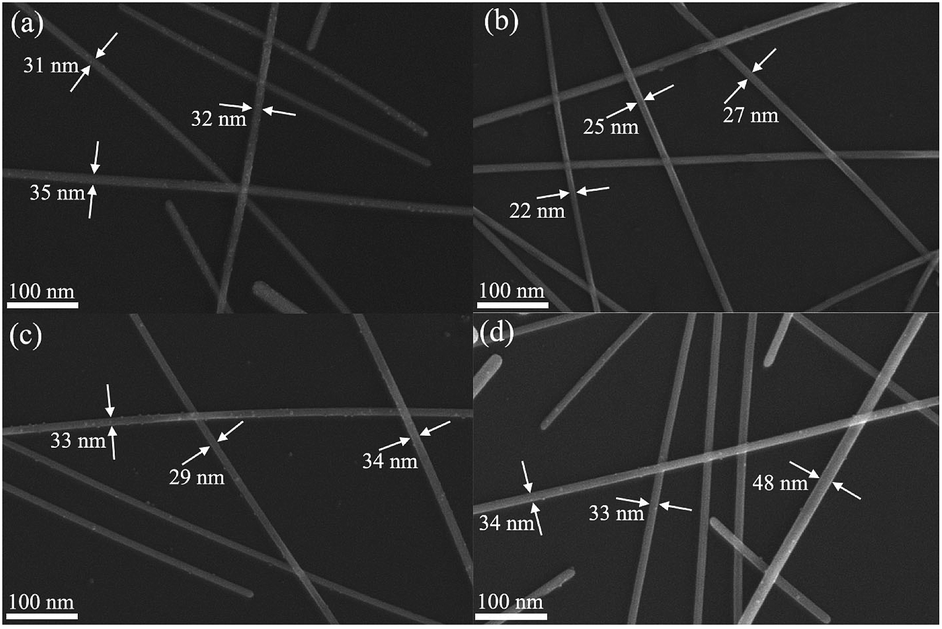 | ||
| Fig. 1 FE-SEM images of AgNWs prepared under different molar ratio of 6CHZB/AgNO3: (a) 0.01, (b) 0.02, (c) 0.03, and (d) 0.04, respectively, reaction temperature = 170 °C. | ||
The effect of reaction temperature on the morphology of AgNWs were further studied, the control experiments at different temperatures were carried out, and the corresponding FE-SEM images of AgNWs preparation were displayed in Fig. 2. When the reaction temperature was 160 °C, the diameter of the finest AgNW was 36 nm (Fig. 2(a)). As increasing the reaction temperature up to 165 °C, the finest diameter of AgNW was 30 nm (Fig. 2(b)). When the reaction temperature was 175 °C, it is clear that the finest diameter of AgNW could reach 26 nm (Fig. 2(d)). By contrast, when the reaction temperature was 170 °C, the AgNWs have the finest diameter of 22 nm (Fig. 2(c)). Based on the above discussion, 0.02 was determined as the optimum molar ratio of 6CHZB/AgNO3 and the optimal reaction temperature was 170 °C. The following discussion below is thereby under these conditions.
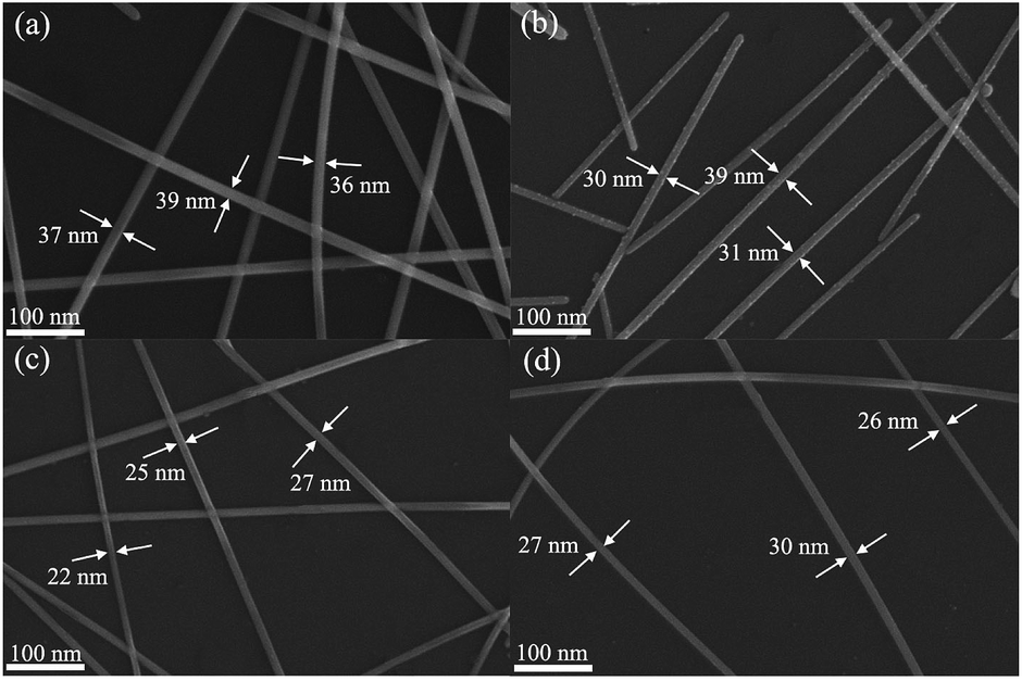 | ||
| Fig. 2 FE-SEM images of AgNWs prepared at different reaction temperatures: (a) 160 °C, (b) 165 °C, (c) 170 °C, and (d) 175 °C, respectively, molar ratio of 6CHZB/AgNO3 = 0.02. | ||
The XRD pattern of the as-synthesized AgNWs is depicted in Fig. 3. The apparent five peaks at 38°, 44°, 64°, 77°, and 81° corresponded to (111), (200), (220), (311), and (222) Bragg reflections of Ag, respectively. By comparing the curve with JCPDS (No. 04-0783) of Ag, it can be fully indexed to a pure phase of face-centered cubic (fcc) Ag crystal (a = b = c = 4.086 Å, space group Fm![[3 with combining macron]](https://www.rsc.org/images/entities/char_0033_0304.gif) m (225)). In addition, no traces of other compounds could be detected, indicating the high purity, which is in good agreement with previous studies.13,14 It is worth noting that the intensity of (111) peak is relatively high, indicating that the AgNWs grew along the (111) Bragg reflection.
m (225)). In addition, no traces of other compounds could be detected, indicating the high purity, which is in good agreement with previous studies.13,14 It is worth noting that the intensity of (111) peak is relatively high, indicating that the AgNWs grew along the (111) Bragg reflection.
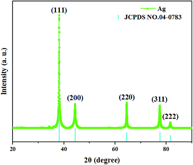 | ||
| Fig. 3 XRD pattern of the as-synthesized AgNWs. | ||
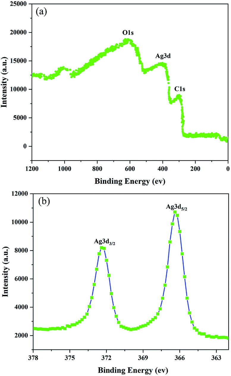
To better understand the chemical composition of the as-synthesized AgNWs, XPS analysis was further carried out, and the results were shown in Fig. 4. Fig. 4(a) is a full-spectrum scan of the as-synthesized AgNWs, which can be clearly found that Ag is the only elements detected except the elements (C, O) from reference substance. The high resolution Ag 3d XPS spectrum shows two prominent peaks around 367 and 373 eV, respectively in good agreement with silver metallic values.15
 | ||
| Fig. 4 XPS spectra of the as-synthesized AgNWs. | ||
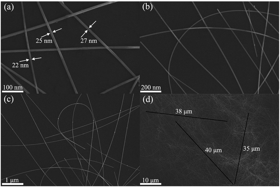
The microscopic morphology of the as-synthesized AgNWs was observed by FE-SEM, and the images of AgNWs at different magnifications are shown in Fig. 5. Fig. 5(a)–(c) clearly shows the structural features of AgNW with a thin and uniform diameter and a narrow size distribution. According to the enlarged FE-SEM image (Fig. 5(a)), the diameter of AgNWs varied from 22 to 27 nm with a narrow size distribution. In addition, one can see that the surface was smooth without tiny structures. As can be seen from Fig. 5(d), the length of the as-synthesized AgNW was estimated to be 35 to 40 μm. More importantly, no other Ag nanostructures such as polyhedrons, spheres and cubes were observed, demonstrating the high uniformity of AgNWs.
 | ||
| Fig. 5 FE-SEM images of AgNWs at different magnifications. | ||
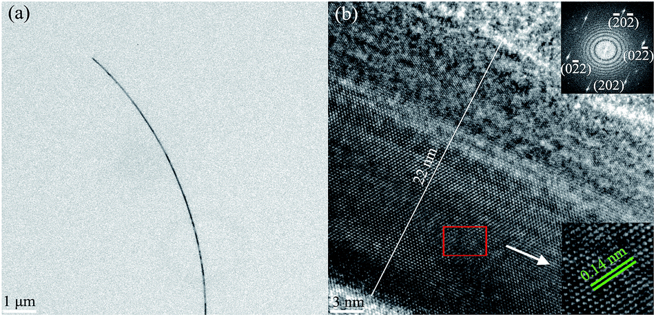
The as-synthesized AgNWs were further characterized by FE-TEM and selected area electron diffraction (SAED) analyses, as shown in Fig. 6. Obviously, the ultra-fine AgNWs have been successfully synthesized. As is clear from Fig. 6(b), AgNW was divided into two halves by a double plane parallel with longitudinal axis, and the insetted SAED pattern further proves that AgNWs has a twin crystalline structure. Further, well-developed lattice fringes having a regular pitch of 0.14 nm can be observed, which was consistent with the separation of Ag (220) crystal plane, and the high crystallinity of the synthesized AgNW was confirmed together with the above XRD analysis.
 | ||
| Fig. 6 FE-TEM images and SAED pattern (inset) of the as-synthesized AgNWs. | ||
To investigate the possible formation mechanism of AgNWs in this work, samples produced at different stages were obtained and the corresponding FE-SEM results were shown in Fig. 7. Firstly, as can be seen from Fig. 7(a), after standing at room temperature for 2 h, almost no substance was visible, suggesting that the reaction did not occur obviously during this process. Second, the silver ions should be reduced to silver atoms on the AgBr particles through EG as shown in Fig. 7(b). In Fig. 7(c), heating was continued and small silver decahedral seeds were formed subsequently on the surface of AgBr particles. When the solution was further heated to 15 min (Fig. 7(d)), the one-dimensional growth of Ag decahedral seeds eventually leads to the formation of AgNWs. Finally, the thick AgNWs continued to grow and produced the ultra-fine AgNWs (Fig. 7(e)).
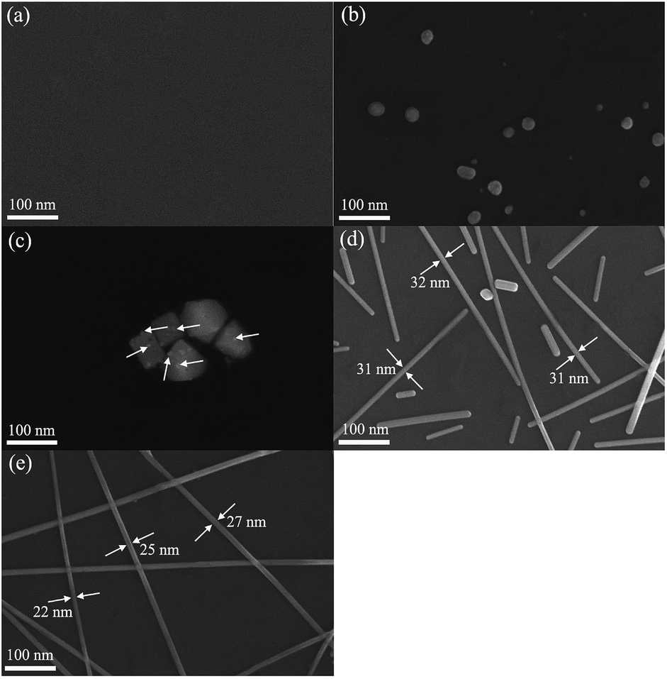 | ||
| Fig. 7 FE-SEM images of samples at different reaction times: (a) standing at room temperature for 2 h, (b) heating for 5 min, (c) heating for 10 min, (d) heating for 15 min, (e) heating for 20 min. | ||
Everyone knows that nano-metals, especially silver, exhibit excessive optical phenomena directly related to surface plasmon resonance (SPR) according to the shape and size of the metals.16 In essence, the UV-vis spectrum can be used to determine the size and shape of the AgNWs because different frequencies correspond to different SPR bands.17 As shown in Fig. 8(a), no apparent absorption peak arose after standing at room temperature for 2 h. The Ag0 nucleis were then formed by heating at 170 °C for 5 minutes (Fig. 8(b)). As can be seen from Fig. 8(c), there were a distinct peak at 417 nm and a slightly tilted peak at wavelength of 600 nm, indicating that nanorods formed at this time, but the number was very small and almost invisible by FE-SEM (Fig. 7(c)). From Fig. 8(d), two distinctly different SPR peaks at 354 nm 371 nm could be seen, indicating that AgNWs were generated after 15 min of reaction at 170 °C. However, the intensity of the SPR peaks at this time was low, implying that only a small amount of AgNWs were produced. As shown in Fig. 8(e), two strong SPR peaks (359 and 368 nm) appeared at significantly shorter wavelengths than the SPR peaks in Fig. 8(d), indicating that a large number of finer AgNWs were eventually synthesized.
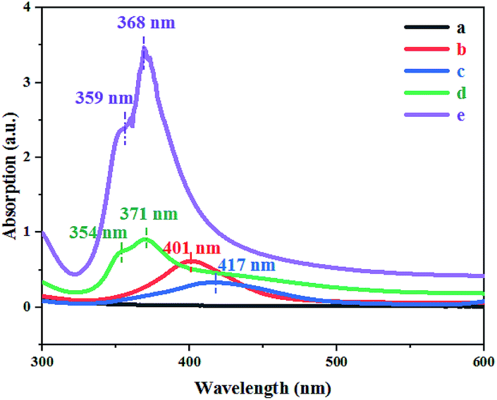 | ||
| Fig. 8 UV-vis absorption spectra of AgNWs at different reaction times: (a) standing at room temperature for 2 h, (b) heating for 5 min, (c) heating for 10 min, (d) heating for 15 min, (e) heating for 20 min. | ||
Based upon the above results and discussions, the possible growth mechanism of AgNWs was proposed, as shown in Fig. 9. In recent years, there were some studies reported that the diameter of AgNWs could be determined by the size of AgBr seed crystal formed in the prime step of the polyol synthesis.18 For the NaBr additive, the diameter of AgNWs between 30 nm and 50 nm were received.19 In this paper, however, it can be clearly seen from Fig. 5(a) that the AgNWs with the diameter < 30 nm even the finest diameter 22 nm were obtained by the 6CHZB assistant polyol process. In this process, 6CHZB should play a very important role, which structure is shown in Fig. 9(b). Because the AgNWs grew on the basis of the silver decahedral seeds formed in the early stage, it could be thus inferred that the 6CHZB additive was more favorable for forming small silver decahedral seeds (Fig. 7(c)). Besides, as is known that the interaction of PVP macromolecule with the {100} facets is stronger than the {111} facets, and this interaction became stronger when the molecular weight of PVP was larger. Also, the bromide ions have been proved to hold an analogous role, adsorbed in the {100} facets, consuming to passivate the newly formed {100} facets, {111} facets at the corner sites would be thereby developed and resulted in the formation of ultrafine AgNWs (Fig. 9(a)).19–23 On the other hand, the molar concentration of 6CHZB also affected the diameter of AgNWs. A suitable molar concentration increased the likelihood of combination of the photoelectron with interstitial silver, Ag+ in the AgBr seed crystals. Eventually, the latent images formed faster in AgBr than that in AgCl, partially owing to the different effective mass of electrons (0.215m0 vs. 0.302m0) and Hall mobility (60 cm2 V−1 s−1 vs. 50 cm2 V−1 s−1) for AgBr and AgCl.24 This may explain why it took a short time to form ultra-fine AgNWs through 6CHZB additive.
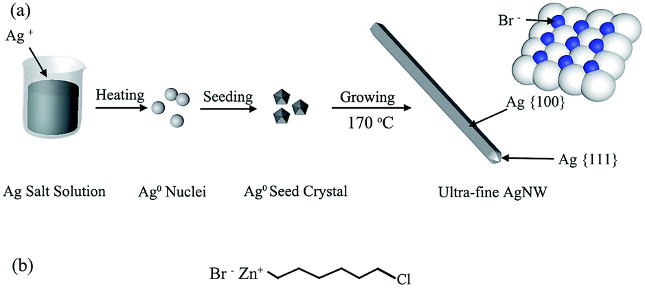 | ||
| Fig. 9 (a) Schematic representation of the proposed growth mechanism of AgNWs, (b) molecular structure of the 6CHZB. | ||
Further, the high-quality AgNWs synthesized by the above method were used to fabricate 2D TCFs by a straightforward bar coating process. Subjectively, as shown in Fig. 10(a), the text below the 2D TCF can be visually observed. In order to verify this phenomenon more scientifically, the transmittance and haze instrument was employed. It can be clearly seen from Fig. 10(d) that the 2D AgNWs film has a high transmittance of 90.3% and an ultra-low haze of 0.99% (Fig. 10(c)). In fact, the AgNWs film formed by the ultrafine AgNWs network was nearly transparent due to the intensity of the scattered light is low. In addition, from Fig. 10(b) we can see that the AgNWs film has a low resistance 48 Ω sq−1, suggesting that the film has a good conductivity, which is sufficient to meet the requirements of electronic components.
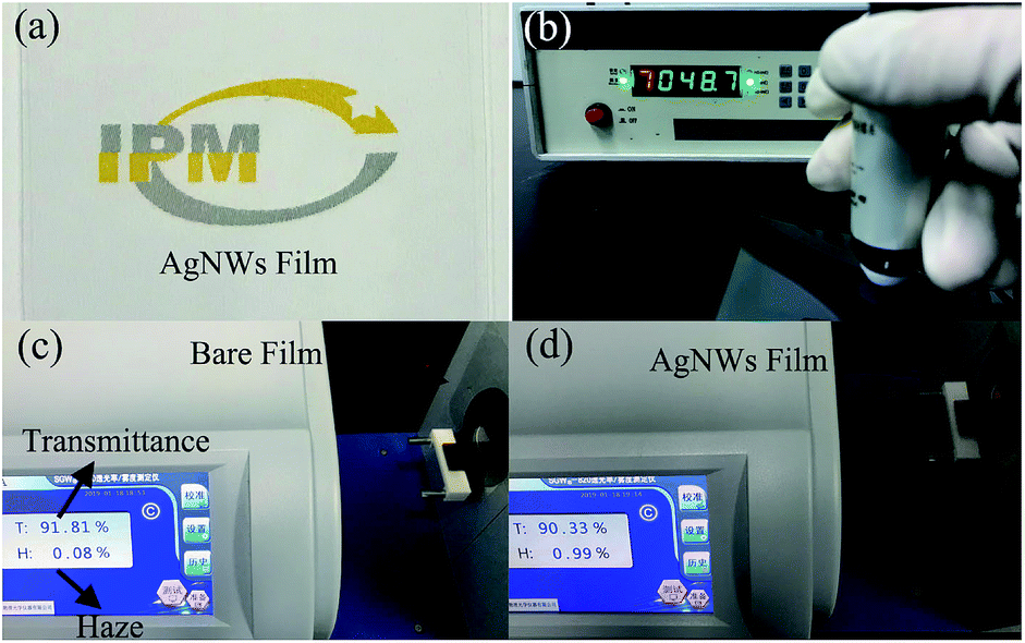 | ||
| Fig. 10 (a) Optical image of the AgNWs film, (b) sheet resistance measurement of the AgNWs film, (c) the transmittance and haze of the bare PET film, (d) the transmittance and haze of the AgNWs film. | ||
4. Conclusion
For the first time, 6CHZB was used as a promoter to successfully synthesize high-quality AgNWs with a diameter of 20 nm and a length of 40 μm. The presence of a moderate amount of 6CHZB has been shown to facilitate the formation of smaller silver decahedral seeds and ultimately to form high quality AgNW. More importantly, transparent conductive film fabricated from AgNWs exhibits a high transmittance of 90.3% and a low haze of <1.0% with a low resistance 48 Ω sq−1, which showed great potential to replace the conventional brittle ITO films.Conflicts of interest
There are no conflicts to declare.Acknowledgements
This work was supported by the National Natural Science Foundation of China (Grant No. 21761016), the Young and Middle-aged Academic and Technical Leaders Reserve Talents Program of Yunnan Province (Grant No. 2017HB060), the Applied Basic Research Foundation of Yunnan Province (Grant No. 2017FB142), the Major R&D Project of Yunnan Province (Grant No. 2018ZE001), the Research Foundation of Key New Products of Yunnan Province (Grant No. 2016BA007), and the Research Foundation of Institute of Yunnan Province (Grant No. 2016DC033).Notes and references
- K. Ellmer, Nat. Photonics, 2012, 6(12), 9–17 CrossRef.
- X. Zhang, X. Yan, J. Chen and J. Zhao, Carbon, 2014, 69, 437–443 CrossRef CAS.
- A. T. Khalil, M. Ovais, I. Ullah, M. Ali, Z. K. Shinwari, S. Khamlich and M. Maaza, Nanomedicine, 2017, 12(15), 1767–1789 CrossRef CAS PubMed.
- P. L. Jun, J. L. Jia, L. Lu, F. Ren, W. Hu, J. Li, S. H. Qi and Q. B. Pei, ACS Nano, 2014, 8(12), 12874–12882 CrossRef PubMed.
- T. Aernouts, P. Vanlaeke, W. Geens, J. Poortmans, P. Heremans, S. Borghs, R. Mertens, R. Andriessen and L. Leenders, Thin Solid Films, 2004, 451(452), 22–25 CrossRef.
- S. Yao and Y. Zhu, Nanoscale, 2014, 6(4), 2345–2352 RSC.
- X. J. Xu, G. T. Fei, X. W. Wang, Z. Jin, W. H. Yu and L. D. Zhang, Mater. Lett., 2007, 61(1), 19–22 CrossRef CAS.
- J. Xu, J. Hu, C. J. Peng, H. L. Liu and Y. Hu, J. Colloid Interface Sci., 2006, 298(2), 689–693 CrossRef CAS PubMed.
- Y. J. Zhu and X. L. Hu, Mater. Lett., 2004, 58(9), 1517–1519 CrossRef CAS.
- T. You, S. L. Xu, S. X. Sun and X. Y. Song, Mater. Lett., 2009, 63(11), 920–922 CrossRef CAS.
- R. R. D. Silva, M. X. Yang, S.-I. Choi, M. F. Chi, M. Luo, C. Zhang, Z. Y. Li, P. H. C. Camargo, S. J. L. Ribeiro and Y. N. Xia, ACS Nano, 2016, 10(8), 7892–7900 CrossRef PubMed.
- E. J. Lee, M. H. Chang, Y. S. Kim and J. Y. Kim, APL Mater., 2013, 105(2), 4211848–4211854 Search PubMed.
- X. L. Tang, M. Tsuji, P. Jiang, M. Nishio, S. M. Jang and S. H. Yoon, Colloids Surf., A, 2009, 338(1–3), 33–39 CAS.
- B. Wu, A. Heidelberg and J. J. Boland, Nano Lett., 2006, 6(3), 468–472 CrossRef CAS PubMed.
- E. Sumesh, M. S. Bootharaju and T. Pradeep, J. Hazard. Mater., 2011, 189(1–2), 450–457 CrossRef CAS PubMed.
- M. A. Khan, A. Qayyum, I. Ahmed, T. Iqbal, A. A. Khan, R. Waleed, B. Mohuddin and M. Malik, Chin. Phys. Lett., 2016, 33(7), 078102 CrossRef.
- Y. L. Wang, T. Herricks and Y. N. Xia, Nano Lett., 2003, 3(8), 1163–1166 CrossRef CAS.
- Q. Zhang, C. H. Moran, X. Xia, M. Rycenga, N. X. Li and Y. N. Xia, Langmuir, 2012, 28(24), 9047–9054 CrossRef CAS PubMed.
- M. Li, M. Jing, Z. Wang, B. Li and X. Q. Shen, J. Nanosci. Nanotechnol., 2015, 15(8), 6088–6093 CrossRef CAS PubMed.
- J. P. Kottmann, O. J. F. Martin, D. R. Smith and S. Schultz, Phys. Rev. B: Condens. Matter Mater. Phys., 2001, 64(23), 235402 CrossRef.
- Y. G. Sun and Y. N. Xia, Analyst, 2003, 128(6), 686–691 RSC.
- Y. J. Rui, W. L. Zhao, D. W. Zhu, H. Y. Wang, G. L. Song, M. T. Swihart, N. Wan, D. W. Gu, X. B. Tang, Y. Yang and T. Y. Zhang, Nanomaterials, 2018, 161(3), 103390 Search PubMed.
- J. F. Hamilton, Adv. Phys., 1988, 37(4), 359–441 CrossRef CAS.
- P. Zhang, Y. L. Wei, M. Ou, Z. Z. Huang, S. D. Lin, Y. Y. Tu and J. W. Hu, Mater. Lett., 2018, 213, 23–26 CrossRef CAS.
| This journal is © The Royal Society of Chemistry 2019 |