
 Open Access Article
 This Open Access Article is licensed under a Creative Commons Attribution-Non Commercial 3.0 Unported Licence
Low-temperature atomic layer deposition of Al2O3/alucone nanolaminates for OLED encapsulation
Guixiong Chen,
Yalian Weng,
Fan Sun,
Xiongtu Zhou *,
Chaoxing Wu,
Qun Yan,
Tailiang Guo and
Yongai Zhang*
*,
Chaoxing Wu,
Qun Yan,
Tailiang Guo and
Yongai Zhang*
College of Physics and Information Engineering, Fuzhou University, Fuzhou 350002, People's Republic of China. E-mail: xtzhou@fzu.edu.cn; yongaizhang@fzu.edu.cn
First published on 4th July 2019
Abstract
Thin film encapsulation (TFE) is one of the key problems that hinders the lifetime and widespread commercialization of flexible organic light-emitting diodes (OLEDs). In this work, TFE of OLEDs with Al2O3/alucone laminates grown by atomic layer deposition (ALD) and molecular layer deposition (MLD) as moisture barriers were demonstrated. The barrier performances of Al2O3/alucone laminates with respect to the individual layer thickness and the number of dyads were investigated. It was found that alucone with suitable layer thickness could reduce the permeation to the defect zones of the inorganic layer by prolonging the permeation pathway, sequentially improving the moisture barrier performance. The water vapor transmission rate (WVTR) could be further lowered with increasing the number of dyads of the laminates, the WVTR value reached 1.44 × 10⁻⁴ g per m2 per day for laminates with 5.5 dyads. These laminates were incorporated in OLEDs with pixel define layer (PDL), and were found to be able to evidently prolong the lifetime of the OLED.
1 Introduction
Organic light-emitting diodes (OLEDs) are considered as one of the most promising display technologies because of their great advantages, such as high efficiency, fast response time and wide viewing angle. In particular, OLEDs are suitable for flexible displays, which are widely accepted as the next-generation display after cathode ray tube (CRT) and flat-panel display (FPD).1 In terms of OLED technology, device encapsulation is the most demanding task because OLEDs require a very high degree of protection from moisture and oxygen permeation. Therefore, gas diffusion barriers with high performance are essential for improving the reliability and lifetime of OLEDs. The conventional encapsulation method has been achieved by sealing the OLED device with a getter in an inert atmosphere using a rigid glass lid or metal, which however, is incompatible with flexible OLED displays.2Thin film encapsulation (TFE) is one of the best developed encapsulation technologies that has been widely developed for flexible encapsulation in recent years. The TFE method has a thinner and lighter form factor, and a higher flexibility of device form during in-flex use.3 Several inorganic thin film barriers, such as Si3N4, SiO2, Al2O3 and TiO2, have been developed for OLEDs encapsulation.4,5 However, thin film barriers consisting of a single-layer normally showed high water vapor transmission rate (WVTR) due to defects in the films caused by the deposition processes and cracks caused by stress when increasing the film thickness. On the other hand, barriers with multilayers comprised of alternating inorganic and organic films were widely used when high barrier performance was required. The incorporation of organic layers could prolong the diffusion pathways and reduce the thin film stress.6,7
A number of approaches to TFE have been developed, atomic layer deposition (ALD) is now being pursued as an alternative to traditional chemical vapor deposition (CVD) and physical vapor deposition (PVD) methods for TFE. ALD is a self-limiting CVD process, which allows for dense and three-dimensional conformal coatings with low number of defects, even at low temperature below 100 °C. In particular, ALD is capable for the fabrication of atomically precise coatings on a variety of surfaces with sub-nanometer precision in film thickness. These features make ALD advantageous to encapsulate the devices with thinner coating, even on the non-planar and/or undulant surfaces.8,9 Indeed, several researches have been reported recently on the multi-layered structure which comprised of alternating layer of different inorganic materials with individual layer thickness in nanometer-scale.10–13 Furthermore, ultra gas-proof polymer hybrid thin layer with WVRT < 10−7 g per m2 per day can be achieved by filling the free volume of the polymer with Al2O3 via gas-phase infiltration using ALD method.14
In order to improve the critical weaknesses of inorganic materials such as cracking and pinhole defects, organic layer can be induced using molecular layer deposition (MLD), which is related to similar self-limiting ALD mechanism. MLD is distinguished from ALD because a molecular fragment can be deposited during the surface reactions, thus the term “molecular” layer deposition has been used to describe this area of work instead of “atomic” layer deposition. The similar deposition mechanisms of ALD and MLD make it possible to combine the two techniques to obtain hybrid inorganic/organic multilayers in the same vacuum chamber. Their composition can be controlled by changing the relative number of ALD and MLD reaction cycles in the reaction sequence, realizing tunable mechanical, chemical, optical, and barrier properties. The ALD/MLD combination structure has been proven to have advanced performances for TFE due to its better film integrity and less defects caused by external factors like sample transfer.15–17 On the other hand, aluminum alkoxides with carbon containing backbones (alucone) fabricated using MLD exhibited superior smoothness with less defect density compared to other organic layers fabricated using spin coating, inkjet printing. The MLD alucone layer could potentially decouple defects and improve the mechanical properties of coating by reducing the internal stress of inorganic films. However, the structure, e.g., the individual layer thickness and the number of stacks, is remained for further improvement.18–20
In this work, Al2O3/alucone with maximum thickness of 102.5 nm have been fabricated using ALD/MLD under a low temperature of 90 °C. The optical and moisture barrier performances were then investigated with respect to the individual layer thickness and the number of stacks. Finally, the barrier performance and three-dimensional conformality of Al2O3/alucone films were confirmed as top barrier of OLED devices with uneven pixel defined layer (PDL).
2 Experimental section
2.1 Fabrication of OLED devices and Al2O3/alucone encapsulation layers
The structures of OLED devices and Al2O3/alucone encapsulation layers are schematically illustrated in Fig. 1a and b. The OLED devices were fabricated by conventional thermal evaporation system (Choshu Industry) under a vacuum of less than 5 × 10⁻⁵ Pa. ITO (8 ohm □−1, 150 nm) was used as anode, and was cleaned with detergent solution, acetone and deionized water, respectively. A pixel define layer (PDL) with groove length × width × height of 165 μm × 60 μm × 1.1 μm was fabricated via photolithography, as shown in Fig. 1c and d. The ITO substrates with PDL were treated by plasma for 3 min, and then transferred to vacuum deposition system. A simple OLED device structure was adopted, where N,N′-bis(naphthalen-1-yl)-N,N′-bis(phenyl)-2,2-diMe (NPD, 50 nm) was used as hole transport layer, tris-(8-quinolato) aluminium (Alq3, 50 nm) was used as light emitting layer and electron transport layer, then lithium fluoride (LiF, 1 nm) and aluminium (Al, 150 nm) were used as electron injection layer and cathode, respectively.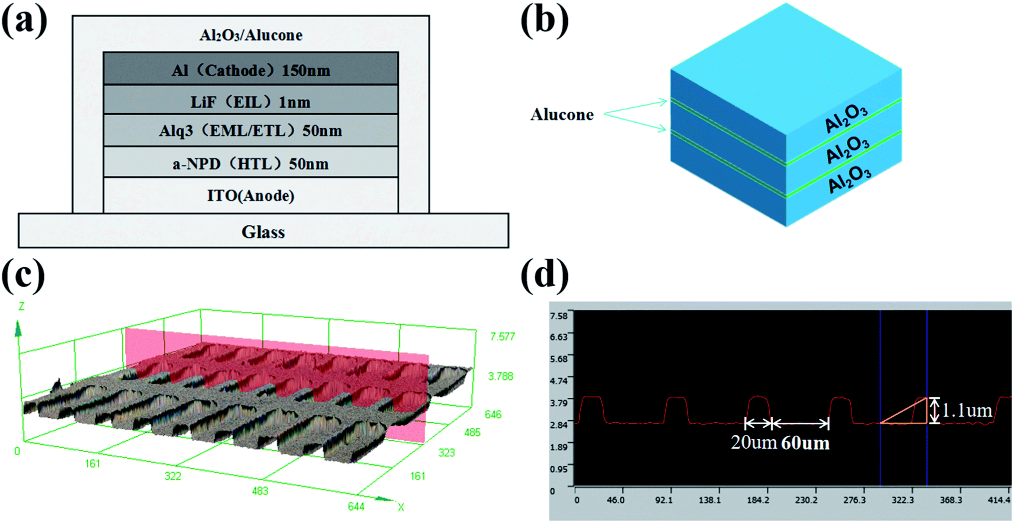 | ||
| Fig. 1 (a) Schematic diagram of an OLED device with TFE. (b) Schematic illustration of Al2O3/alucone 15–2.5 encapsulation layers. (c) The 3D topography of PDL. (d) The height profiles (red line) taken along a typical row of PDL. | ||
Inorganic/organic multilayer barrier films were deposited on the top surface of OLED devices using ALD (Beneq TFS-200) with precisely controlled thickness under the temperature of 90 °C for encapsulation. For preparation of Al2O3 thin films, trimethylaluminum (TMA) and water (H2O) were used as the precursors, with high purity N2 (99.999%) as the carrier gas with flow rate of 20 sccm. A single Al2O3 cycle comprised the following steps: TMA pulse for 0.2 s, N2 purging for 6 s, H2O pulse for 0.15 s and N2 purging for 10 s. Alucone thin films were deposited in the same reactor with TMA and ethylene glycol (EG) as the precursors, before the deposition process, EG was preheated to 60 °C to increase its vapor pressure, the sequence of pulses for a single alucone cycle was as follows: TMA pulse for 0.15 s, N2 purging for 6 s, EG pulse for 0.5 s and N2 purging for 20 s.
Thickness of thin films was measured with both ellipsometry (J.A.Woollam, W-VASE) and field emission scanning electron microscope (FE-SEM, FEI Nova NanoSEM 230, 10 kV acceleration voltage) to determine more precisely the growth per cycle (GPC) of both Al2O3 and alucone films. Then, the ALD sequences were repeated to obtain the desired thicknesses. Thin film barriers with different Al2O3/alucone structure were investigated. For clarity, barriers with alternate Al2O3/alucone of 50/0 nm (single Al2O3 thin film), 22.5/5/22.5 nm, 15/2.5/15/2.5/15 nm, 9/1/9/1/9/1/9/1/9/1 nm and 0/50 nm (single alucone thin film) were denoted as film A50–0, A22.5–5, A15–2.5, A9–1 and A0–50, respectively. The structure of film A15–2.5 was shown in Fig. 1b.
2.2 Characterizations
The composition of Al2O3 was confirmed by X-ray photoelectron spectroscopy (XPS) using an ESCALab250 electron spectrometer (VG USA) with the incident radiation of Al Kα, the binding energies were referenced to the C 1 s line at 284.6 eV of carbon. The morphology of thin films were analyzed by an atomic force microscope (AFM, Bruker Multimode 8) in contact mode to determine their uniformity and surface roughness. The transmittance of the films were measured using UV-vis spectrophotometer (Shimadzu, UV-3600). The luminance of the devices were measured with an spectrophotometer (TOPCON, SR-LEDW). The counting of undamaged pixels were processed using ImageJ software (version 1.51, NIH). The Indentation Modulus was tested by using nano-indentation tester (Anton Paar NHT2) in Oliver model.WVTR measurements were carried out to test the barrier performance of the films through the calcium (Ca) corrosion method.21 Briefly, the amount of water vapor permeating through the film was estimated with the following formula:
3 Results and discussion
3.1 Deposition of Al2O3 and alucone films under low temperature
The GPC of both Al2O3 and alucone with respect to the growth temperature were investigated, as shown in Fig. 2a. It was found that with increasing growth temperature, the GPC for Al2O3 films increased, while the GPC for alucone films decreased. The GPC for alucone films decreased with increasing growth temperature could be attributed to enhanced precursor desorption at high temperature, since the ALD reaction is thermally activated.22–24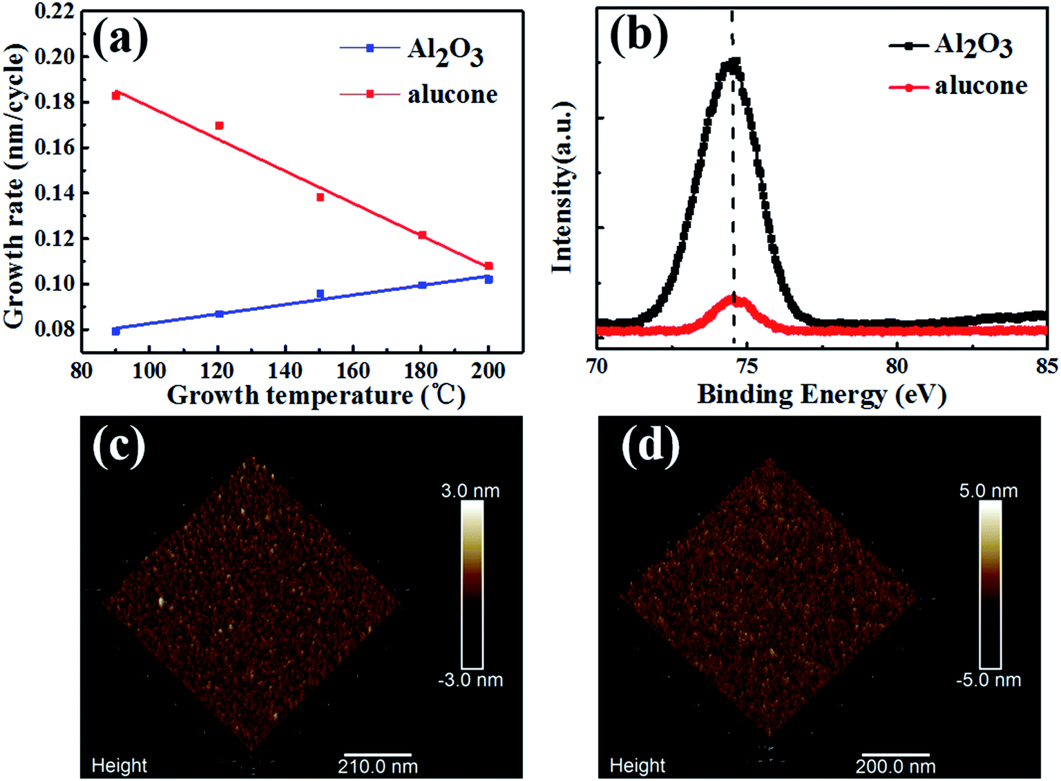 | ||
| Fig. 2 (a) The growth rate (thickness per cycle) of ALD Al2O3 and MLD alucone as a function of reaction chamber temperature. (b) The high resolution binding energy spectrum of Al 2p in the XPS spectra of Al2O3 and alucone. AFM images of film Al2O3 (c) and alucone (d) grown on Si substrate under the temperature of 90 °C. | ||
In order to avoid or to reduce the influence of high temperature on the OLED devices, the encapsulation layers were fabricated under low-temperature of 90 °C. X-ray photoelectron spectroscopy (XPS) and atomic force microscope (AFM) measurements were carried out to examine the composition and morphology of Al2O3 and alucone thin films. As shown in Fig. 2b, the binding energy of Al 2p for Al2O3 and alucone were located at 74.4 eV and 74.55 eV, respectively, which agrees well with that of Al2O3 and alucone in the previous reports.25–27 It was also found that both the Al2O3 and alucone films were very smooth, with root-mean-squared (RMS) surface roughness values (1 × 1 μm2) of 0.352 nm and 0.66 nm for Al2O3 and aluconefilms, respectively, as illustrated in Fig. 2c and d. It was confirmed that both Al2O3 and alucone films were grown successfully under low temperature of 90 °C.
3.2 Optimization of Al2O3/alucone structures and their barrier performance
The single-layer Al2O3 and alucone films prepared by ALD and MLD show smooth surface morphology with less pinholes compared to those fabricated using other methods such as physical vapor deposition (PVD) and plasma enhanced chemical vapor deposition (PECVD).5,18 However, due to the intrinsic defects, such as microcracks and pinholes, these single-layer encapsulation films could only reduce the oxygen and water permeation rates by two to three orders of magnitude from the permeation rate values of bare plastic substrate, which is far from the requirements of OLED application. Inorganic/organic nanolaminates that consist of alternating inorganic and organic multilayers are promising when high-barrier performance is required.14In order to evaluate the effects of individual layer thickness on the encapsulation performance, calcium films were deposited over the Al2O3/alucone laminates with total thickness of 50 nm and various alucone thickness were investigated. Single-layer Al2O3 and alucone films were also studied for reference. For clarity, barriers with alternate Al2O3/alucone of 50/0 nm (single-layer Al2O3 film), 22.5/5/22.5 nm, 15/2.5/15/2.5/15 nm, 9/1/9/1/9/1/9/1/9/1 nm and 0/50 nm (single-layer alucone film) were denoted as film A50–0, A22.5–5, A15–2.5, A9–1 and A0–50, respectively. The WVTR was determined using calcium test, and the results were plotted as normalized resistivity (R0/R) vs. time curve, as shown in Fig. 3a. The values of WVTR calculating from the slope of each linear fitting curve were 2.25 × 10⁻² g per m2 per day, 1.43 × 10⁻² g per m2 per day, 2.51 × 10⁻³ g per m2 per day, 1.01 × 10⁻² g per m2 per day, 6.88 × 10⁻² g per m2 per day for the samples of A50–0, A22.5–5, A15–2.5, A9–1 and A0–50, respectively. It was found that Al2O3/alucone nanolaminated structures exhibited superior barrier performance to single Al2O3 or alucone films with the same total thickness. This improvement might be attributed to the synergetic effect of confinement of the permeation to the defect zones of single-layer materials, providing longer diffusion paths of permeant molecules. The permeation of water vapor was also significantly affected by the thickness distribution of Al2O3 and alucone. Although all the samples of A22.5–5, A15–2.5 and A9–1 consisted of 45 nm Al2O3 and 5 nm alucone, the sample of A15–2.5 exhibited better barrier performance than that of A22.5–5 and A9–1. The incorporation of alucone interlayers were considered to be able to prolong the permeation path way by filling the defects of Al2O3 layer and form chemical bonds with better adhesion between the Al2O3 and alucone layers. However, for sample A22.5–5, there was only one alucone layer, and the improvement of barrier performance was limited. For the sample A9–1, although there was five alucone layers, the thickness of alucone layer was only 1 nm, which might be insufficient to effectively fill the defects of Al2O3 layer. It was concluded that appropriate thickness and layers number of alucone could improve the barrier performance of Al2O3/alucone laminates.
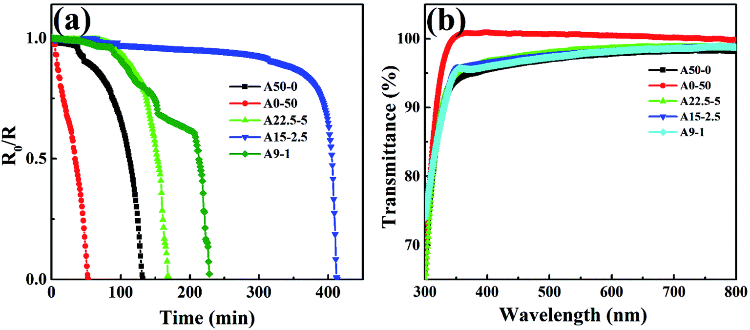 | ||
| Fig. 3 (a) Dependence of the normalized conductance vs. time of the Ca corrosion tests of Al2O3/alucone films in a controlled environment of 25 °C and 60% RH. (b) Transmittance of different Al2O3/alucone films. | ||
Spectrophotometry was also used to measure the optical transmission properties of the samples. The used Al2O3 and alucone films, as well as the Al2O3/alucone laminates were highly transparent in the visible region, as shown in the Fig. 3b. All the samples showed light transmission of above 95%, which could be attributed to the lower surface roughness. This result demonstrated that besides the barrier on the substrates, Al2O3/alucone laminates may also be suitable for the barrier on the top surface of top-emitting OLED devices.
To further study the influences of alucone layer on the barrier performance, Al2O3/alucone laminates with Al2O3 thickness of 15 nm and alucone thickness of 2.5 nm (A15–2.5) were tailored by varying the number of stacks, the results were also plotted as normalized resistivity (R0/R) vs. time curve, as shown in Fig. 4. It was found that the water barrier properties were enhanced with the increase of the dyad (1 Al2O3 layer + 1 alucone layer) of laminates. The WVTR calculating from the slope of each linear fitting curve were 1.74 × 10⁻² g per m2 per day, 2.47 × 10⁻³ g per m2 per day, 6.41 × 10⁻⁴ g per m2 per day, 2.23 × 10⁻⁴ g per m2 per day and 1.44 × 10⁻⁴ g per m2 per day for Al2O3/alucone laminates of 1.5, 2.5, 3.5, 4.5 and 5.5 dyads, respectively. After that, the (R0/R) = f(t) curves fell dramatically because of sudden occurrence of defects in the thin film barrier, which might be caused by particles, or gases from the reaction of Ca with moisture (oxygen), as well as cracks induced by stress changes.
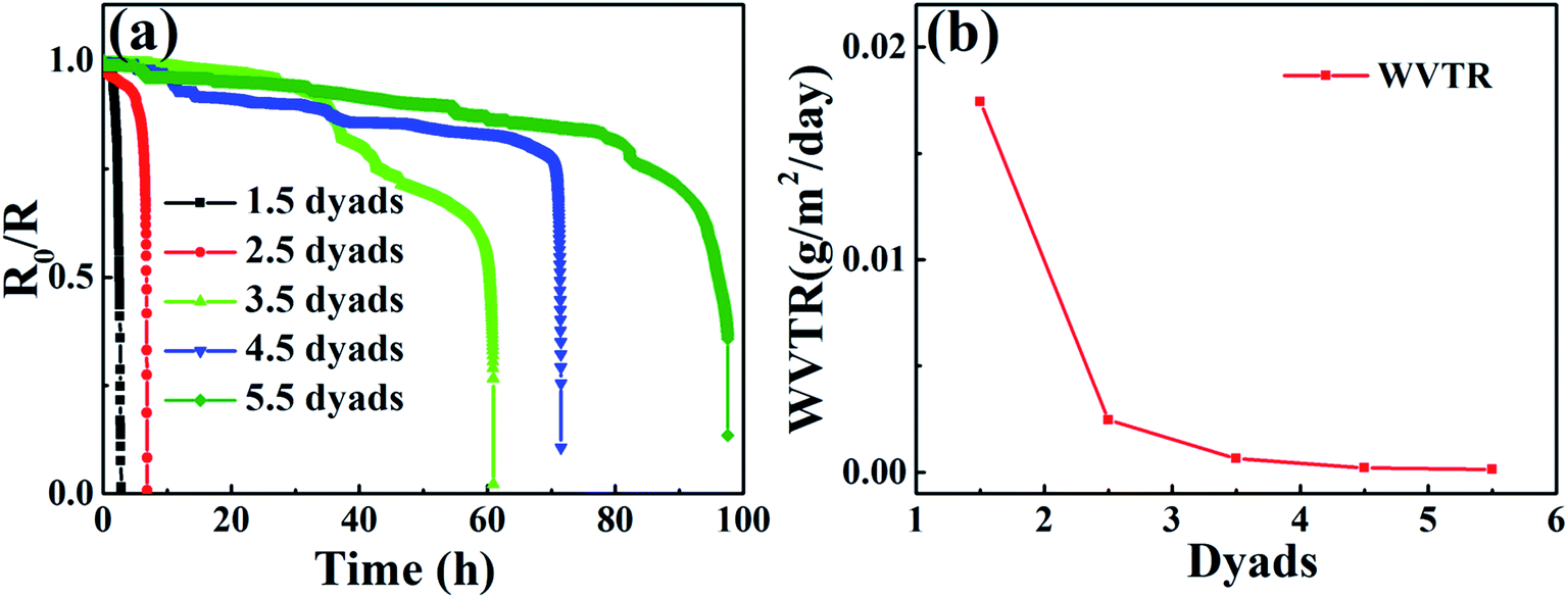 | ||
| Fig. 4 (a) Dependence of the normalized conductance vs. time of the Ca corrosion tests with different dyads of Al2O3/alucone films in a controlled environment of 25 °C and 60% RH. (b) The curve of WVTR changed with different dyads. | ||
The WVTR of the Al2O3/alucone laminates (A15–2.5, 102.5 nm) was comparable with three pairs of hybrid Al2O3 (15 nm)/ZrO2 (15 nm)/alucone (80 nm).19 Commercially, in order to assure the minimum lifetime of most OLEDs at least for 10000 h, the WVTR should be less than 10−6 g per m2 per day.2 Al2O3/alucone laminates with more number of dyads and thickness should be used.
3.3 Lifetime of green OLEDs and the degradation behaviors
The water barrier properties of the Al2O3/alucone laminates were further verified using a subsequent evolution of electroluminescence (EL) from green OLEDs with various laminate dyads, as shown in Fig. 5. All measurements were taken under the same conditions, where the applied DC voltage was 5 volts and the initial EL intensity L0 was 300 cd m−2. From Fig. 5a, it was confirmed that the TFE showed little effect on the EL of devices (intensity and wavelength) compared to bare OLED, which is a requisite for the TFE of OLEDs. It is assumed that the small degree of decreased EL intensity is associated with the thermal annealing during the ALD process. It was obvious that the decay of EL intensity became less abrupt with increasing the dyad of Al2O3/alucone laminates, as shown in Fig. 5b. Without TFE encapsulation, the time where the EL intensity, plotted as normalized intensity (L/L0) vs. time curve, fell 50% below its initial value (L/L0 = 0.5) was around 50 hours. With increasing the dyads of Al2O3/alucone laminates, the lifetime extended. For the sample encapsulated with 5.5 dyads, the luminance kept more than 60% after 380 hours compared to that of its initial value. These degradation behaviors were consistent with the WVTR results, and were in agreement with previous reports, which was normally attributed to unstable fluorescence quenchers.28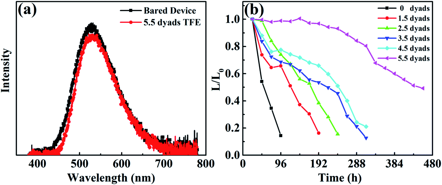 | ||
| Fig. 5 (a) EL spectrum of bared OLED device (without encapsulation) and device with TFE of 5.5 dyads Al2O3/alucone films at the bias voltage of 5 volts. (b) Normalized luminance of the OLED devices vs. time for samples without encapsulation (0 dyad) and with various TFE of Al2O3/alucone films. | ||
Pixel define layer (PDL) was often used in the OLED industry for fabrication of colorful (RGB) devices. However, the PDL will lead to sags and steps on the device surface, which raises higher requirements for the encapsulation. As depicted in Section 2.1, PDL has also been set in this work in order to evaluate the isotropic encapsulation performance of the Al2O3/alucone laminates. Furthermore, the PDL can avoid the sudden degradation because of defects in the thin film barrier, and is useful for analyzing the degradation behaviors of OLED. Al2O3/alucone laminates with various dyads were incorporated with OLED, then the luminance and the lighting states of the samples were tracked over time to observe the black spots and areas caused by the moisture penetration. In consistent with the luminance results (Fig. 5), with increasing the laminate layers, the black spots and areas were obviously suppressed. Fig. 6 illustrates the typical photographs of the samples with 1.5 dyads and 5.5 dyads Al2O3/alucone laminates at different exposing times. It was found that the samples encapsulated with Al2O3/alucone of less dyads (e.g. 1.5 dyads), moisture penetrated from both the edge of PDL and the pinholes, leading to black areas on the edge of pixels, and black spots in the pixels. These black spots and areas were spread rapidly, and only 20% of pixels remained undamaged on the 4th day. With increasing the dyad of Al2O3/alucone laminates, the penetration was improved remarkably due to the high density and good isotropic homogeneity of ALD process. With a 5.5-dyad laminates, few black dot in the pixels appeared two days later, most of damaged pixels were destroyed from the edge. The spreading speed of black areas on the edge of pixels slow down compared to that with a 1.5-dyad laminates, around 70% of the pixels remained undamaged on the 55th day. It could then be assumed that the failure encapsulation of the OLED devices lie in the shadow areas caused by steps or defects such as particle. Fig. 6f illustrate the decreasing tendency of undamaged pixels with time for OLEDs with different TFE. It was also demonstrated that only 102.5 nm of Al2O3/alucone laminates can mainly encapsulate the pixel areas, showing good encapsulation performances of Al2O3/alucone laminates fabricated using ALD. However, thicker laminates should be needed to encapsulate effectively the edge of pixels.
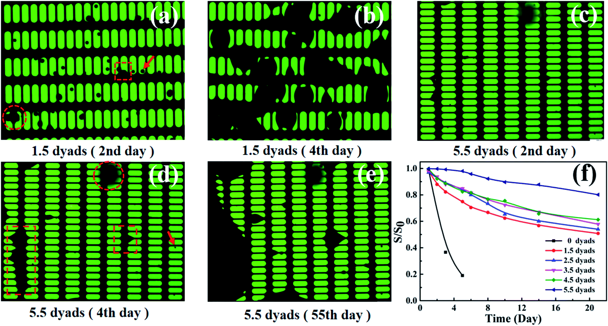 | ||
| Fig. 6 The evolution of pixel images of OLED devices with 1.5 dyads and 5.5 dyads of TFE at different time. (a) 1.5 dyads TFE on the second day, (b) 1.5 dyads TFE on the fourth day, (c) 5.5 dyads TFE on the second day, (d) 5.5 dyads TFE on the fourth day, (e) 5.5 dyads TFE on 55th day. The dash rectangles mark the black areas on the edge of pixels, the red arrows mark the black dots in the pixels, and the dash circles mark a stain in the image view for fixing the same position in the samples. (f) The proportion of undamaged pixels of OLED devices vs. time for different TFE. | ||
3.4 Mechanical properties of Al2O3/alucone structures
Mechanical properties is one of the important concerns of TFE, the elastic modulus and bending behaviours of Al2O3/alucone laminates with 5.5 dyads were also tentatively evaluated by nanoindentation measurements and flexural load. The load versus displacement curves for various measurements of Al2O3/alucone laminate (5.5 dyads) were illustrated in Fig. 7a, from which the elastic modulus and hardness were derived as 64.77 ± 10.65 GPa and 4.9 ± 1.6 GPa, respectively. The elastic modulus of laminates decreased remarkably compared to that of Al2O3 films (380 Gpa),29,30 which could increase the degree of flexibility, since the alucone layers might serve as a stress buffer layer during bending process. Al2O3/alucone laminates (5.5 dyads) deposited on PET substrates with thickness of 0.175 mm were used for the investigation of bending behaviours. The samples were loaded manually along a tube with radii of 4 mm and 12 mm, as schematically shown in the inset of Fig. 7b. During flexural load, the samples develop the sides of a concave and a convex curvature, causing continuous compressive or tensile stress to the substrates. Assume that the centraxonial position would not have elongation during bending test, the laminates set on the convex sides will suffer from elongation of around 2.14% and 0.72% for bending radii of 4 mm and 12 mm, respectively. From the microscopic picture, the laminates showed little damage after more than 200 cycles of bending for bending radius of 12 mm. When reducing the bending radius, some parallel cracks appeared after 40–50 cycles of bending for bending radius of 4 mm, as shown in Fig. 7b. It could be deduced that the Al2O3/alucone laminates might be available for flexible display devices with minimum bending radius around 12 mm.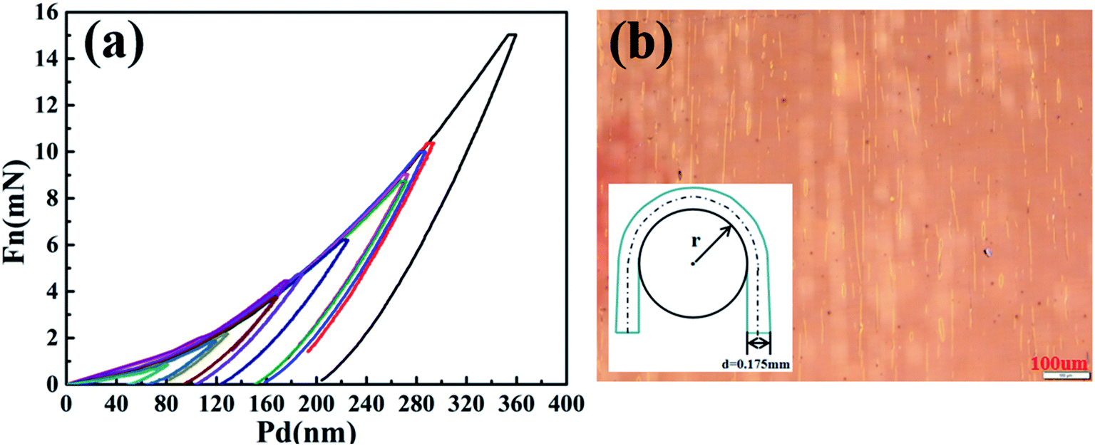 | ||
| Fig. 7 (a) Nanoindentation measurements showing load versus displacement curves for various Al2O3/alucone laminates (5.5 dyads). (b) The microscopic pictures for Al2O3/alucone laminates on PET substrate after 50 cycles of bending (r = 4 mm), the inset show the scheme of bending process, the dash line indicates the centraxonial position of the sample. | ||
4 Conclusions
In summary, Al2O3/alucone laminates were successfully grown under the low temperature of 90 °C using atomic layer deposition (ALD) and molecular layer deposition (MLD), showing dense and smooth surfaces. The barrier performances of Al2O3/alucone laminates with respect to the individual layer thickness and the number of dyads were investigated. It was found that alucone with suitable layer thickness could reduce the permeation to the defect zones of the inorganic layer by prolonging the permeation path way, sequentially improve the moisture barrier performance. The water vapor transmission rate (WVTR) could be further lower with increasing the dyad of the laminates, the WVTR value reached 1.44 × 10⁻⁴ g per m2 per day for laminates with 5.5 dyads. Their barrier performances were further demonstrated by tracking the active areas of organic light-emitting diodes (OLEDs) with thin film encapsulation using various Al2O3/alucone laminates, and were found to able to prolong the lifetime of OLED evidently.Conflicts of interest
The authors declare no conflict of interest.Acknowledgements
This work was financially supported by the National Natural Science Foundation of China (No. 61775038), the National Natural Science Foundation of Fujian Province, China (2017J01758), and the Program for New Century Excellent Talents in Fujian Province University. The content of this work is the sole responsibility of the authors.References
- S. M. Lee, J. H. Kwon, S. Kwon and K. C. Choi, IEEE Trans. Electron Devices, 2017, 64, 1922–1931 CAS.
- D. Yu, Y. Q. Yang, Z. Chen, Y. Tao and Y. F. Liu, Opt. Commun., 2016, 362, 43–49 CrossRef CAS.
- Y. C. Han, E. G. Jeong, H. Kim, S. Kwon, H. G. Im, B. S. Bae and K. C. Choi, RSC Adv., 2016, 6, 40835–40843 RSC.
- E. K. Park, S. Kim, J. Heo and H. J. Kim, Appl. Surf. Sci., 2016, 370, 126–130 CrossRef CAS.
- K. W. Park, S. Lee, H. Lee, Y. H. Cho, Y. C. Park, S. G. Im and S. H. K. Park, RSC Adv., 2019, 9, 58–64 RSC.
- K. H. Yoon, H. S. Kim, K. S. Han, S. H. Kim, Y. E. K. Lee, N. K. Shrestha, S. Y. Song and M. M. Sung, ACS Appl. Mater. Interfaces, 2017, 9, 5399–5408 CrossRef CAS PubMed.
- R. Grover, R. Srivastava, M. N. Kamalasanan and D. S. Mehta, RSC Adv., 2014, 4, 10808–10814 RSC.
- M. Park, S. Oh, H. Kim, D. Jung, D. Choi and J. S. Park, Thin Solid Films, 2013, 546, 153–156 CrossRef CAS.
- M. U. Jewel, M. D. S. Mahmud, M. A. Monne, A. Zakhidov and M. Y. Chen, RSC Adv., 2019, 9, 1841–1848 RSC.
- V. Chawla, M. Ruoho, M. Weber, A. Abou Chaaya, A. A. Taylor, C. Charmette, P. Miele, M. Bechelany, J. Michler and I. Utke, Nanomaterials, 2019, 9, 88 CrossRef PubMed.
- P. Han, T. C. Lai, M. Wang, X. R. Zhao, Y. Q. Cao, D. Wu and A. D. Li, Appl. Surf. Sci., 2019, 467, 423–427 CrossRef.
- F. Romo-Garcia, H. J. Higuera-Valenzuela, D. Cabrera-German, D. Berman-Mendoza, A. Ramos-Carrazco, H. Tiznado, G. A. Hirata, O. E. Contreras and R. Garcia-Gutierrez, Thin Solid Films, 2019, 669, 419–424 CrossRef CAS.
- C. Giovinazzo, C. Ricciardi, C. F. Pirri, A. Chiolerio and S. Porro, Appl. Phys. A: Mater. Sci. Process., 2018, 124, 686 CrossRef.
- L. Lee, K. H. Yoon, J. W. Jung, H. R. Yoon, H. Kim, S. H. Kim, S. Y. Song, K. S. Park and M. M. Sung, Nano Lett., 2018, 18, 5461–5466 CrossRef CAS PubMed.
- B. J. Kim, H. Park, H. Seong, M. S. Lee, B. H. Kwon, D. H. Kim, Y. I. Lee, H. Lee, J. I. Lee and S. G. Im, Adv. Eng. Mater., 2017, 19, 1600819 CrossRef.
- I. Cora, Z. Baji, Z. Fogarassy, Z. Szabo and B. Pecz, Mater. Sci. Semicond. Process., 2019, 93, 6–11 CrossRef CAS.
- J. Li, J. Wu, J. Liu and J. Sun, Nanoscale Res. Lett., 2019, 14, 75 CrossRef PubMed.
- W. Xiao, D. Y. Hui, C. Zheng, D. Yu, Y. Y. Qiang, C. Ping, C. L. Xiang and Z. Yi, Nanoscale Res. Lett., 2015, 10, 1–7 CrossRef CAS PubMed.
- H. Zhang, H. Ding, M. Wei, C. Li, B. Wei and J. Zhang, Nanoscale Res. Lett., 2015, 10, 1–5 CrossRef PubMed.
- M. Park, S. Oh, H. Kim, D. Jung, D. Choi and J. S. Park, Thin Solid Films, 2013, 546, 153–156 CrossRef CAS.
- Y. Weng, G. Chen, X. Zhou, Q. Yan, T. Guo and Y. Zhang, Nanotechnology, 2019, 30, 085702 CrossRef CAS PubMed.
- M. D. Groner, F. H. Fabreguette, J. W. Elam and S. M. George, Chem. Mater., 2004, 16, 639–645 CrossRef CAS.
- D. W. Choi, M. Yoo, H. M. Lee, J. Park, H. Y. Kim and J. S. Park, ACS Appl. Mater. Interfaces, 2016, 8, 12263–12271 CrossRef CAS PubMed.
- C. Hossbach, F. Nehm, A. Singh, H. Klumbies, D. Fischer, C. Richter, U. Schroeder, M. Albert, L. Müller-Meskamp, K. Leo, T. Mikolajick and J. W. Bartha, J. Vac. Sci. Technol., A, 2015, 33, 01A119 CrossRef.
- K. H. Yoon, H. Kim, Y. E. K. Lee, N. K. Shrestha and M. M. Sung, RSC Adv., 2017, 7, 5601–5609 RSC.
- C. Fares, F. Ren, E. Lambers, D. C. Hays, B. P. Gila and S. J. Pearton, J. Electron. Mater., 2019, 48, 1568–1573 CrossRef CAS.
- X. Li, X. Xiong, T. Li, T. Gao and Y. Wu, IEEE Electron Device Lett., 2018, 39, 1952–1955 CAS.
- J. Wu, F. Fei, C. Wei, X. Chen, S. Nie, D. Zhang, W. Su and Z. Cui, RSC Adv., 2018, 8, 5721–5727 RSC.
- J. Nohava, R. Musalek, J. Matejicek and M. Vilemova, Surf. Coat. Technol., 2014, 240, 243–249 CrossRef CAS.
- W. C. Oliver, J. Mater. Res., 1992, 7, 1563–1583 CrossRef.
| This journal is © The Royal Society of Chemistry 2019 |