
 Open Access Article
 This Open Access Article is licensed under a Creative Commons Attribution-Non Commercial 3.0 Unported Licence
Gallium–tin alloys as a low melting point liquid metal for repetition-pulse-laser-induced high energy density state toward compact pulse EUV sources†
Christopher Stephen Andrew Musgrave‡
 ,
Nan Lu,
Rie Sato and
Keiji Nagai*
,
Nan Lu,
Rie Sato and
Keiji Nagai*
Laboratory for Chemical and Life Sciences, Institute of Innovative Research, Tokyo Institute of Technology, R1-26 Suzukake-dai, Midori-ku, Yokohama 226-8503, Japan. E-mail: nagai.k.ae@m.titech.ac.jp
First published on 7th May 2019
Abstract
Here, we show the easy-handling of a liquid gallium–tin alloy (Ga![[thin space (1/6-em)]](https://www.rsc.org/images/entities/char_2009.gif) :Sn) as a laser target source for 13.5 nm light generation. The alloys have ∼30 °C freezing points according to a differential scanning calorimetry cooling process. A Nd:YAG laser (1064 nm, 1 ns, 7.1 × 10¹⁰ W cm−2) ablated the alloys, obtaining a similar extreme ultraviolet emission intensity to Sn despite a small quantity of Sn. Finally, we demonstrate a liquid metal alloy jet and droplets using a plastic nozzle for high-repetition target supply.
:Sn) as a laser target source for 13.5 nm light generation. The alloys have ∼30 °C freezing points according to a differential scanning calorimetry cooling process. A Nd:YAG laser (1064 nm, 1 ns, 7.1 × 10¹⁰ W cm−2) ablated the alloys, obtaining a similar extreme ultraviolet emission intensity to Sn despite a small quantity of Sn. Finally, we demonstrate a liquid metal alloy jet and droplets using a plastic nozzle for high-repetition target supply.
Liquid metals have generated interest in relation to electronics due to the possibilities of producing flexible circuitry, moldable parts, and stretchable electrodes.1 Liquid metals can dissolve other metal ions, often further lowering the melting point through bond disruption.1b In particular, gallium has shown strong potential as it exists readily in a liquid state at room temperature, with a non-oxygenated bulk and non-toxic properties. For example, gallium-based catalysts are exciting in terms of CO2 reduction.1c
A cruder, but no less interesting, way of using liquid metals is in laser plasma generation. Laser plasma sources are of interest in fields such as extreme ultraviolet lithography (EUVL) and quantum beam generation.2 EUVL generation is a process whereby a material, typically tin, is heated by a high-intensity laser pulse to ∼100 eV. The energy losses from the laser pulse (IL) are excess heating to high ionization (Iion), greater kinetic energy of ions and electrons (Ikin), and out-of-band radiation (Ioobrad) as follows:2e
| IL = Ikin + Iion + Irad + Ioobrad | (1) |
In order to obtain the most favorable wavelength of 13.5 nm for the lithography optics, tin is the best element with the highest Irad under optimized conditions.2e
The light produced by this heating will be applied in the high volume manufacturing of semiconductors as a lithographic process. Currently, commercial EUVL sources are supplied as a test tool for lithography; powers at the intermediate focus are ever increasing (>125 W), and the source is highly available (>80%).3 However, more is needed from EUVL sources due to the need for higher throughput.4 Furthermore, practical issues remain problematic, such as the durability issue of the reflective optics.4,5
In addition to EUVL, compact EUV sources with different target sources, such as gas puff targets6 and low-density materials,7 are becoming attractive. These sources should be low cost, allowing exploration of different applications such as surface modification of materials8 and time-resolved ultraviolet photoelectron spectroscopy (UPS) studies, etc. By combining high-power laser compactness9 and emerging target materials and technologies,7e,10 reliable quantum beam sources can be developed. Overall, laser plasma target materials play an important role in producing very high temperature plasmas, X-ray and higher quantum beam emission.
To date, many works have focused on the technical optimization of EUV, such as the laser and target parameters.10,11 However, optimizing the target source could be just as beneficial for EUV and other laser plasma sources; for example clever target design can improve laser conversion efficiency (CE).11f This area is firmly established with the chemical synthesis of these low-density targets.7f,10,11b,11f The plasma generated from well-defined low-density targets have lower self-reabsorption than full-density targets.11a Dilution of tin is also an effective method for obtaining a high CE by-polymer,11d and lithium dilution.11f One criticism of minimum mass and well-defined low-density targets is that large laser systems would require a substantial design modification in order to be accommodated. However, an alternative dilution by a liquid metal droplet source would not suffer the same issues as liquid tin. This could be easily adapted to existing EUV design protocols, and should be considered for larger laser plasma sources. Furthermore, construction of new generations of EUV sources based on a low melting point liquid alloy would be simpler than liquid tin. Low melting point metals such as gallium or indium have caught the interest of EUV researchers.12 One alloy that heavily utilizes gallium, commercially known as Galinstan®, is typically composed of Ga (62–95%), In (5–22%) and Sn (0–16%), and has a strong emission of 13.5 nm light due to the presence of Sn.12a Therefore, Galinstan® could be highly desirable as a target source for EUVL given the very low reported melting point of −19 °C. However, low CE and the broad and flat shaped EUV spectrum due to the presence of indium (∼15/16 nm) and gallium (∼11/12 nm) restricts Galinstan® to metrology applications.12b For EUV, the choice between utilization of gallium or indium is a decision for researchers. Such as a 50:50% Sn:In alloy has the same density as liquid Sn, and a melting point of ∼155 °C.13 On the other hand, gallium has a lower melting point than indium, meaning that alloys of gallium–tin could remain liquid at temperatures less than 100 °C. Although gallium has been mentioned on patents,14 there is a lack of accessible experimental data to assess the viability of gallium alloys as an EUV source.
The aim of this work was to demonstrate that Ga:Sn alloys are an easy-handling liquid metal alternative to Sn as a laser plasma target source. Ga:Sn alloys of differing atomic (at%) ratios were synthesized, then characterized using differential scanning calorimetry (DSC) and scanning electron microscopy (SEM) with X-ray dispersive spectroscopy (EDS). A Nd:YAG laser (1 ns, 2 mJ) was used to generated EUV under similar conditions to previous work,15 with a grazing incidence spectrometer (GIS). As an example, we show that EUV emission intensity for the Ga:Sn alloy was equal to bulk Sn, depending on the alloy composition. The CE for the Ga:Sn alloy was also estimated in comparison with bulk tin using a calorimeter. We also show the emission properties of the alloy irradiated by 10 Hz exposure in order to demonstrate the potential as a practical and flexible laser plasma target source. Finally, our progress developing Ga:Sn jets and droplets is shown.
DSC data shown in Fig. S1–S4† exhibit consistency with the phase diagram reported;16 the endothermic peak on the liquidus and exothermic peaks at the solidus (27 °C), and supercooling solidus from the metastable state (–25 °C) are shown in Table 1.
:Sn alloy composition (at%), estimated melting points (°C), and conversion efficiency (CE) (%) at 13.5 nm 2% bandwidth
| Ga:Sn composition |
Melting point (°C) | Freezing point (°C) | CE (%) | |
|---|---|---|---|---|
| Atomic% prepared | Atomic% ratio measured by EDS | |||
| a Literature value.b EDS mapping struggled to correlate well to the prepared atomic percentage, however the EUV data suggested the correct composition was obtained. | ||||
| 0:100 |
N/A | 232a | 1.3 | 1.3 |
| 100:0 |
N/A | 29a | 0.5 | 0.5 |
| 90:10 |
90:10 ± 2 |
22 | −9 | 0.8 |
| 80:20 |
89:11b ± 2 |
30 | 60, −25 | 1.0 |
| 70:30 |
74:26 ± 3 |
30 | 80, −25 | 1.3 |
| 60:40 |
66:34 ± 4 |
30 | 90, −25 | 1.3 |
In order to utilize the alloy as a laser target, more detailed characterization is necessary, such as the microstructure of the metastable phase and stability. SEM was used to image the 10 at% Ga:Sn alloy surface structure, while the EDS probe measured the elemental composition (at%). SEM revealed the globular alloy microstructure (Fig. 1), which appeared as a distinctive light (tin) and dark (gallium) spotted pattern. More examples of such architectural features can be found in the ESI.† The island-sea-like globular microstructure of the alloy is one of several typical structures formed by alloys. Here, the globular structure is composed of heterogeneous sized ‘islands’ of tin surrounded by a gallium ‘sea’. These tin ‘islands’ typically vary from 20 μm to 200 μm in diameter. We were required to apply additional carbon tape to image the lower tin at% containing alloys due to electron beam charge up, and difficulties associated with imaging semi-molten samples.
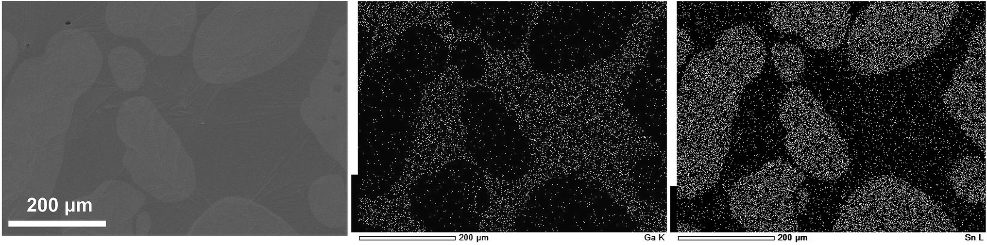 | ||
| Fig. 1 SEM image (left) and EDS maps (Ga, middle and Sn, right) from a Ga:Sn = 90:10 at% alloy on a glass substrate. The globule islands are composed of tin, surrounded by gallium. Unlike the SEM images, the lighter grey patterning represents the element measured by the EDS probe in each case. | ||
From the phase diagram, the SEM images at room temperature (Fig. S5–S8†) are characterized as eutectic phases with an island-sea structure. On the whole, the alloys were in a metastable semi-molten state on the surface of the glass substrate at 25 °C. The molten alloy was easy to handle, and unreactive in air. This is because of the properties of the mother metals, which is an attractive quality of the alloy. Furthermore, the sub 100 °C melting point meant that plastic nozzles could be used for the injection systems. For high-repetition (kHz) EUV generation, a further study examining the alloy debris properties is pertinent.
The EDS probe revealed the elemental at% composition, which is consistent with the ratio of Sn and Ga (Fig. S9–S12† and Table 1). One small issue we had during characterization was measuring the at% elemental composition data for the Ga:Sn 80:20% alloy. The SEM images showed the alloyed regions, and mapped tin in a higher quantity than 90:10%, yet the EDS measurement was performed multiple times on several samples and could not resolve 80:20% at%. The reason for this was uncertain, other than potentially insufficient EDS probe resolution. On the other hand, the EUV data indicated that the correct alloy ratio was fabricated due to the intensity of the spectra obtained in comparison to lower and higher Sn% alloys. If the incorrect ratio was synthesized, it would have been evident from the EUV intensities. However, the EUV intensity of 80:20% Ga:Sn was measured between the intensities of 90:10% and 70:30% Ga:Sn (Fig. 2).
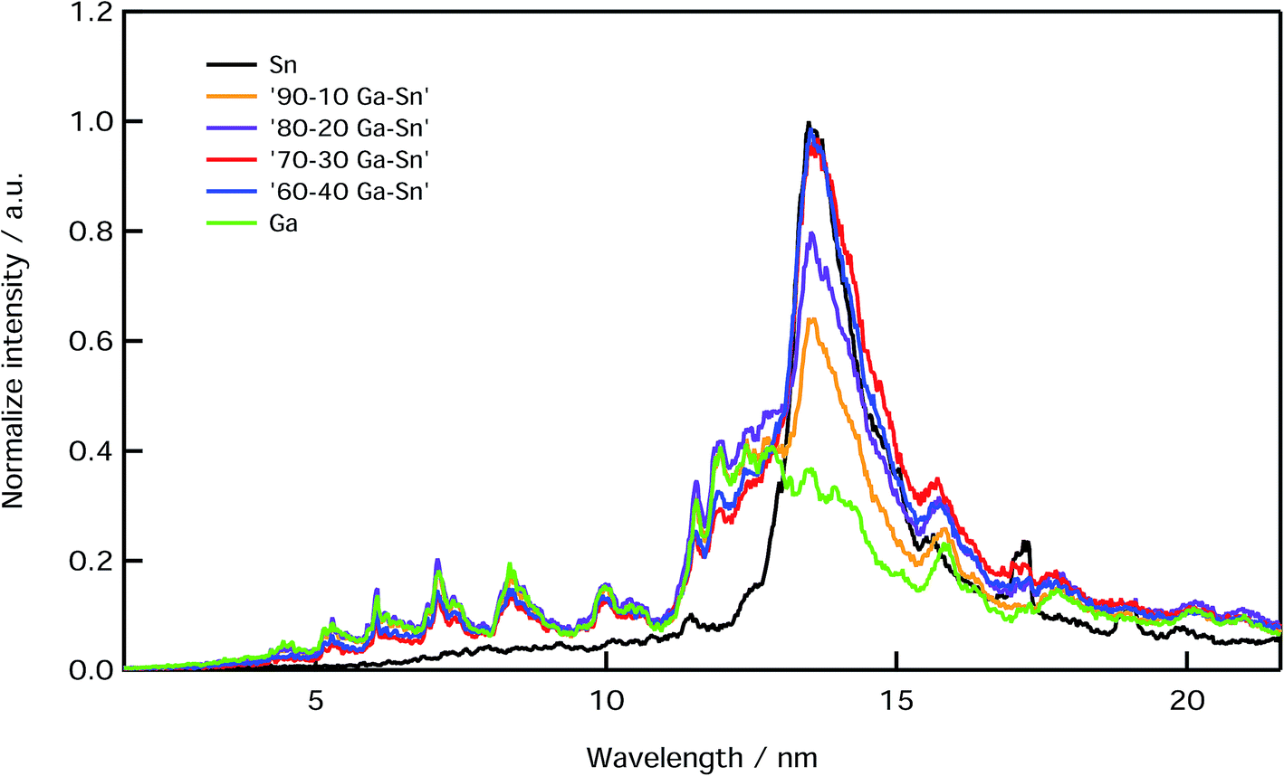 | ||
| Fig. 2 Spectra overlay of the relative EUV emission intensities of the Ga:Sn alloys and reference metals ablated using a laser intensity of 7.1 × 10¹⁰ W cm−2. | ||
Fig. 2 shows the overlaid EUV spectra for all the Ga–Sn alloys, and Sn and Ga reference metals. Tin EUV emissions have been described as an unresolved transmission array (UTA) from Sn8+ to Sn21+ from 4d–4f transmissions.17 Gallium UTA emission in the 13.5 nm region arises from Ga8+ to Ga11+ from 3p–3d transitions, and 3d–4p transitions of Ga8+.12a In the case of the Ga:Sn alloys, a large UTA across 11–15 nm was observed with a distinctive peak at 13.5 nm arising from tin transmissions, as detailed above.
The emission intensity at 13.5 nm reached a plateau at 30% tin content, as shown in Fig. S13.† We confirmed this by observing that there was very little difference between the intensities of 30% and 40% Sn content and bulk Sn. The Ga EUV emissions for the alloys containing 30% and 40% tin can still be seen in the ∼11–13 nm region. This established that the alloys were ablated in the alloyed region instead of a tin island, which we would expect to be devoid of strong Ga emissions.
The increasing intensity of the peak at 13.5 nm as the tin content increased was an expected trend. Based on this, we anticipated that a feasible EUV source could be composed of a Ga:Sn alloy with as low as 30–40% Sn content. This alloy would also have the advantage of keeping the liquid metal target source at around 40 °C. On the other hand, gallium metal had a significantly lower CE at 13.5 nm (0.5% vs. 1.3% Sn). This was expected given the low relative intensity of the emission at 13.5 nm 2% bandwidth. We did not investigate alloys with more than 50% tin content due to the increasing melting point, without corresponding increases in the EUV intensity at 13.5 nm.
We were concerned with the ‘island-sea’ heterogeneity of the alloys, not only the SEM images but also in generating EUV. Developing a low melting point alloy with inconsistent EUV emission properties would not be practical. Generally, alloy heterogeneity was not an issue we encountered, but it was possible to obtain such inconsistent emission intensities after trial and error (Fig. 3(a) and (b)). In each case, the spectrum was dominated by one metal rather than emission properties from both metals. For the gallium-dominated emission (Fig. 3(a)), there was still a distinctive emission at 13.5 nm which can be attributed to the solvated tin atoms present (0–10% at% Sn content) in the gallium. We considered that the laser spot ablated a very small alloyed region. The tin-dominated spectra (Fig. 3(b)) had a strong emission around 13.5 nm due to large volume of tin ablated. To further test the alloy, we performed 10 Hz exposure experiments using an auto-stage to ablate the fresh alloy during laser exposure (Fig. 3(c)). The resulting EUV emission was more representative of the higher tin content alloys rather than ablating a large region of a single metal. We confirmed the location of the 10 Hz emission by SEM (Fig. 4). The laser spot encompassed the alloyed region of the alloy, deforming the surface approximately to the diameter of the laser spot size. The consistency of the 10 Hz emission was encouraging for higher repetition EUV emission. A refined synthesis of the alloy would reduce any inconsistency relating to emission intensity. This would therefore retain high-power output at the intermediate focus, while retaining a sub 100 °C melting point.
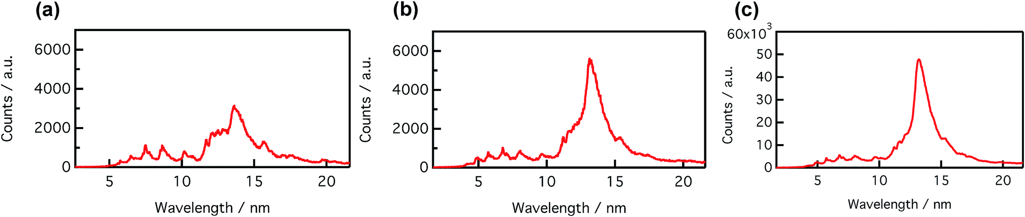 | ||
| Fig. 3 Single shot EUV emission of a Ga:Sn alloy in two different locations (a) and (b), and a 10 Hz emission (c) of the same target. An auto-stage was used to ensure fresh target was ablated during a 10 Hz exposure at 2.5 × 10¹⁰ W cm−2. The shifting speed of the target was 2 mm s−1. | ||
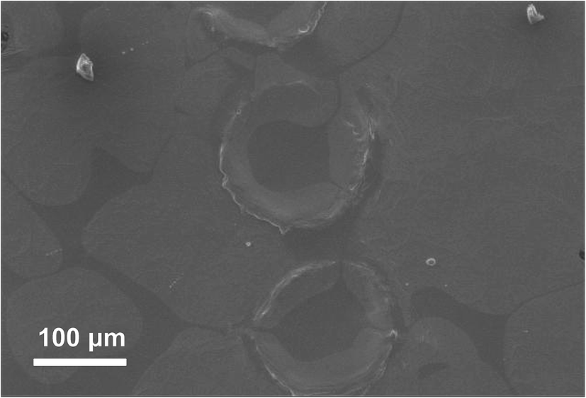 | ||
| Fig. 4 SEM micrograph of the ablation trace on a Ga:Sn alloy using 10 Hz exposure from a Nd:YAG laser region. | ||
Alloy oxidation generally was an issue for EUV generation, even though oxidation occurs after sample preparation from the surface.11f,15 Oxygen has a characteristic EUV peak at 17 nm, that only grows with increasing Sn content (Fig. 2). In fact, this peak was not observed during the 10 Hz experiments. Perhaps the gallium oxide layer was significantly thinner than tin oxide, and thus did not affect EUV generation until higher Sn content was reached.
Although the reduced melting point is a step forward for handling the alloy target source, SEM revealed that all alloys had a heterogeneous globular structure. Our concern for this alloy as an EUV light source material stems from its practical use. For example, producing inconsistent power at the intermediate focus due to ablation of larger amounts of one metal in the alloy is very undesirable. Exploring improved synthesis processes to produce a more homogeneous globular structure would be highly attractive. Finally, we used a polytetrafluoroethylene (PTFE) nozzle (inner diameter of 150 μm) and syringe pump to produce Ga:Sn droplets or a liquid Ga:Sn jet. To achieve Ga:Sn droplets or a jet we controlled the pump rate of the apparatus between 1.1 mL min−1 and 2 mL min−1, respectively (Fig. 5). This is an important aspect of laser plasma generation, especially where requirements range from Hz to kHz speeds, depending on the application.3 Ablation of alloy droplets could suit slower repetition rates, whereas a jet could satisfy higher repetition needs. From a practical perspective, PTFE nozzles were necessary due to gallium amalgam chemistry. Amalgamation of common metal nozzles such as aluminum could risk damage to the nozzle, or target supply contamination with the amalgamated metal. Moreover, the low melting point of the alloys opened up the possibility of using plastic components. This is difficult currently due to the high temperature required for maintaining liquid tin (232 °C). This could be attractive on a more industrial scale for laser plasma generation.
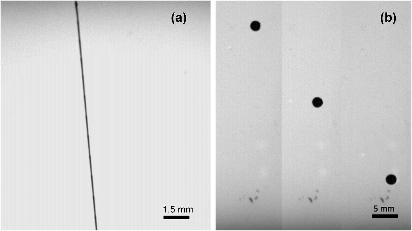 | ||
| Fig. 5 CCD camera images of Ga:Sn capturing below 100 mm of a syringe containing the Ga:Sn (a) at 10 °C and (b) at 30 °C. The exposure time was 0.1 ms and the duration among the image was 10 ms for (b). The nozzle of the syringe was PTFE with inner and outer diameters of 150 μm and 760 μm, respectively. | ||
In summary, we showed that liquid metal Ga:Sn alloys are promising as a laser plasma target source. The Ga:Sn alloys have a wide metastable temperature region when compared with liquid tin (>30 °C vs. > 232 °C). An area of future focus would be to reduce alloy eutectic issues that could affect performance as a source of EUV light. By selecting the alloy ratio, we could obtain the EUV emission properties without significant loss of performance compared with bulk tin. Our data indicated that 30 at% content was necessary for an estimated melting point of ∼30 °C and CE of 1.3% (vs. 1.3% bulk tin), striking an ideal balance between the two metals. We performed 10 Hz exposures, and plastic nozzle injection tests demonstrated the potential for this material from a practical point of view as a laser plasma target source for quantum beam sources.
Conflicts of interest
There are no conflicts to declare.Acknowledgements
We thank Grant-in-Aid for Scientific Research (KAKENHI) and the Dynamic Alliance for Open Innovation Bridging Human, Environmental and Materials from MEXT. We also thank the Suzukakedai Materials Analysis Division, Technical Department, Tokyo Institute of Technology, for assistance with SEM-EDS and DSC analysis.Notes and references
- (a) M. D. Dickey, ACS Appl. Mater. Interfaces, 2014, 6, 18369 CrossRef CAS PubMed; (b) T. Daeneke, K. Khoshmanesh, N. Mahmood, I. A. de Castro, D. Esrafilzadeh, S. J. Barrow, M. D. Dickey and K. Kalantar-Zadeh, Chem. Soc. Rev., 2018, 47, 4073 RSC; (c) D. Esrafilzadeh, A. Zavabeti, R. Jalili, P. Atkin, J. Choi, B. J. Carey, R. Brkljaca, A. P. O'Mullane, M. D. Dickey, D. L. Officer, D. R. MacFarlane, T. Daeneke and K. Kalantar-Zadeh, Nat. Commun., 2019, 10, 865 CrossRef PubMed.
- (a) N. M. Ceglio, A. M. Hawryluk and G. E. Sommargren, Appl. Opt., 1993, 32, 7050 CrossRef CAS; (b) C. Wagner and N. Harned, Nat. Photonics, 2010, 4, 24 CrossRef CAS; (c) R. Peters, S. Lok, E. van Alphen, N. Harned, P. Kuerz, M. Lowisch, H. Meijer, D. Ockwell, E. van Setten, G. Schiffelers, J.-W. van der Horst, J. Stoeldraijer, R. Kazinczi, R. Droste, H. Meiling and R. Kool, Proc. SPIE, 2013, 8679, 86791F CrossRef; (d) T. Ito and S. Okazaki, Nature, 2000, 406, 1027 CrossRef CAS PubMed; (e) K. Nishihara, et al., Phys Plasmas, 2008, 15, 056708 CrossRef.
- A. Pirati, R. Peeters, D. Smith, S. Lok, M. van Noordenburg, R. van Es, E. Verhoeven, H. Meijer, A. Minnaert, J.-W. van der Horst, H. Meiling, J. Mallmann, C. Wagner, J. Stoeldraijer, G. Fisser, J. Finders, C. Zoldesi, U. Stamm, H. Boom, D. Brandt, D. Brown, I. Fomenkov and M. Purvis, Proc. SPIE, 2016, 9776, 97760A–97762A Search PubMed.
- H. Mizoguchi, H. Nakari, T. Abe, K. M. Nowak, Y. Kawasuji, H. Tanaka, Y. Watanabe, T. Hori, T. Kodama, Y. Shirasishi, T. Yanagida, Y. Yamada, T. Yamazaki, S. Okazaki and T. Saitou, Proc. SPIE, 2017, 10097, 1009702 CrossRef.
- (a) A. L. Klein, W. Bouwhuis, C. W. Visser, H. Lhuissier, C. Sun, J. H. Snoeijer, E. Villermaux, D. Lohse and H. Gelderblom, Phys. Rev. Appl., 2015, 3, 044018 CrossRef; (b) K. Tomita, Y. Sato, S. Tsukiyama, T. Eguchi, K. Uchino, K. Kouge, H. Tomuro, T. Yanagida, Y. Wada, M. Kunishima, G. Soumagne, T. Kodama, H. Mizoguchi, A. Sunahara and K. Nishihara, Sci. Rep., 2017, 7, 12328 CrossRef PubMed.
- P. W. Wachulak, Rev. Sci. Instrum., 2016, 87, 091501 CrossRef PubMed.
- (a) T. Okuno, S. Fujioka, H. Nishimura, Y. Tao, K. Nagai, Q. Gu, N. Ueda, T. Ando, K. Nishihara, T. Norimatsu, N. Miyanaga, Y. Izawa and K. Mima, Appl. Phys. Lett., 2006, 88, 161501 CrossRef; (b) S. S. Harilal, M. S. Tillack, Y. Tao, B. O'Shay, R. Paguio and A. Nikroo, Opt. Lett., 2006, 31, 1549 CrossRef CAS PubMed; (c) L. Ge, K. Nagai, Z. Gu, Y. Shimada, H. Nishimura, N. Miyanaga, Y. Izawa, K. Mima and T. Norimatsu, Langmuir, 2008, 24, 10402 CrossRef CAS PubMed; (d) Q. Gu, K. Nagai, T. Norimatsu, S. Fujioka, H. Nishimura, K. Nishihara, N. Miyanaga and Y. Izawa, Chem. Mater., 2005, 17, 1115 CrossRef CAS; (e) K. Nagai, C. S. A. Musgrave and W. Nazarov, Phys. Plasmas, 2018, 25, 030501 CrossRef; (f) K. Nagai, Q. Gu, Y. Yasuda, T. Norimatsu, S. Fujioka, H. Nishimura, N. Miyanaga, Y. Izawa and K. Mima, J. Polym. Sci., Part A: Polym. Chem., 2009, 47, 4566 CrossRef CAS.
- A. Bartnik, H. Fiedorowicz, R. Jarocki, J. Kostecki, M. Szcurek, O. Chernyayeva and J. W. Sobczak, J. Electron Spectrosc. Relat. Phenom., 2011, 184, 270 CrossRef CAS.
- G. A. Mourou, T. Tajima and S. V. Bulanov, Rev. Mod. Phys., 2006, 78, 309 CrossRef CAS.
- S. Yuspeh, Y. Tao, R. A. Burdt, M. S. Tillack, Y. Ueno and F. Najmabadi, Appl. Phys. Lett., 2011, 98, 201501 CrossRef.
- (a) M. Yamaura, S. Uchida, A. Sunahara, Y. Shimada, H. Nishimura, S. Fujioka, T. Okuno, K. Hashimoto, K. Nagai, T. Norimatsu, K. Nishihara, N. Miyanaga, Y. Izawa and C. Yamanaka, Appl. Phys. Lett., 2005, 86, 181107 CrossRef; (b) H. Lan, H. Lei, D. Zuo, X. Wan and G. Zheng, Vacuum, 2017, 135, 86 CrossRef CAS; (c) T. H. Dinh, Y. Suzuki, R. Hirose, H. Hara, H. Ohashi, B. Li, P. Dunne, G. O'Sullivan, A. Sunahara and T. Higashiguchi, Rev. Sci. Instrum., 2014, 85, 116104 CrossRef PubMed; (d) S. Namba, S. Fujioka, H. Nishimura, Y. Yasuda, K. Nagai, N. Miyanaga, Y. Izawa, K. Mima and K. Takiyama, Appl. Phys. Lett., 2006, 88, 171503 CrossRef; (e) K. Nagai, Q. Gu, Z. Gu, T. Okuno, S. Fujioka, H. Nishimura, Y. Tao, Y. Yasuda, M. Nakai, T. Norimatsu, Y. Shimada, M. Yamaura, H. Yoshida, M. Nakatsuka, N. Miyanaga, K. Nishihara and Y. Izawa, Appl. Phys. Lett., 2006, 88, 094102 CrossRef; (f) K. Nagai, C. S. A. Musgrave, N. Kuwata and J. Kawamura, ACS Omega, 2018, 3, 12422–12427 CrossRef CAS.
- (a) B. Li, H. Hara, Y. Suzuki, G. Arai, T. Higashiguchi, H. Ohashi, W. Jiang, T. Makimura, H. A. Sakaue, C. Suzuki, D. Kato, I. Murakami, P. Dunne, E. Long, P. Sheridan, X. Chen and G. O`Sullivan, J. Appl. Phys., 2015, 118, 073302 CrossRef; (b) I. Tobin, L. Juschkin, Y. Sidelnikov, F. O'Reilly, P. Sheridan, E. Sokell and J. G. Lunney, Appl. Phys. Lett., 2013, 102, 203504 CrossRef.
- D. Kurilovich, A. L. Klein, F. Torretti, A. Lassie, R. Hoekstra, W. Ubachs, H. Gelderblom and O. O. Versolato, Phys. Rev. Appl., 2016, 6, 014018 CrossRef.
- (a) N. R. Bowering, O. V. Khodykin, A. N. Bykanov, I. V. Fomenkov, US2006/0249699 A1, United States, 2006; (b) L. Yuning, W. Xinbing, Z. Duluo, L. Peixiang, CN105333953B, China, 2016.
- C. S. A. Musgrave, T. Murakami, T. Ugomori, K. Yoshida, S. Fujioka, H. Nishimura, H. Atarashi, T. Iyoda and K. Nagai, Rev. Sci. Instrum., 2017, 88, 033506 CrossRef PubMed.
- T. J. Anderson and I. Ansara, J. Phase Equilib., 1992, 13, 181–189 CrossRef CAS.
- Y. Shimada, H. Nishimura, M. Nakai, K. Hashimoto, M. Yamaura, Y. Tao, K. Shigemori, T. Okuno, K. Nishimura, T. Kawamura, A. Sunahara, T. Nishikawa, A. Sakai, K. Nagai, T. Norimatsu, S. Fujioka, S. Uchida, N. Miyanaga, Y. Izawa and C. Yamanaka, Appl. Phys. Lett., 2005, 86, 051501 CrossRef.
Footnotes |
| † Electronic supplementary information (ESI) available: Detailed synthesis, experimental procedures and characterisation data are given. See DOI: 10.1039/c9ra01905g |
| ‡ Present address: Centre of Micro/Nano Manufacturing Technology (MNMT-Dublin), University College Dublin, D14 YH57, Dublin, Ireland. |
| This journal is © The Royal Society of Chemistry 2019 |