
 Open Access Article
 This Open Access Article is licensed under a Creative Commons Attribution-Non Commercial 3.0 Unported Licence
Influence of defect structure on colour tunability and magneto optical behaviour of WO3 nanoforms
Kriti  a,
Puneet Kaura,
Simranpreet Kaura,
Deepawali Aroraa,
K. Asokanb and
D. P. Singh*a
a,
Puneet Kaura,
Simranpreet Kaura,
Deepawali Aroraa,
K. Asokanb and
D. P. Singh*a
aDepartment of Physics, Guru Nanak Dev University, Amritsar-143005, India. E-mail: dpsingh.phy@gndu.ac.in
bMaterials Science Division, Inter University Accelerator Centre, Aruna Asaf Ali Marg, New Delhi-110067, India
First published on 2nd July 2019
Abstract
The present study reports the impact of thermal annealing on the structural, optical and magnetic properties of WO3 nanostructures, synthesized using an acid precipitation method by, employing various spectroscopic and magnetic measurements. The X-ray diffraction and Raman measurements confirmed the orthorhombic structure of as dried WO3·H2O and monoclinic structure of WO3 nanopowders annealed at or above 500 °C. The morphological characterization shows the formation of different microstructures like nanosheets, nanoplatelets and nanocuboids in the micro-scale with the variation of annealing temperatures. The optical band gap has been calculated using the Kubelka–Munk function. The room temperature photoluminescence (PL) spectra recorded at different excitation wavelengths show intense near ultraviolet (NUV) emission which might be due to the presence of localized states associated with oxygen vacancies, and the surface states in the conduction band. The emissions in visible region correspond to the structural defects such as oxygen vacancies present within the band gap and band to band transitions. The spectral chromaticity colour coordinates indicate that the light emitted from the prepared samples shows shift from violet to red region with the change of excitation wavelength. Magnetic measurements show decrease in room temperature ferromagnetism (FM) with annealing temperature. The X-ray absorption spectroscopy (XAS) measurements at O K-edge show the significant change in the W–O hybridizations. The decrease in PL intensity and ferromagnetic ordering with increase in annealing temperatures are directly correlated with the filling up of oxygen vacancies in the samples. The oxygen vacancies based F-Center exchange model is discussed to understand the origin of FM in WO3 nanostructures.
1 Introduction
The tuning of the physical properties of transition metal oxide (TMO) semiconductors has been a major topic of interest from both fundamental and technological points of view. These nanostructure oxides possess enhanced performance of their functionalities with unique properties that do not exist in their bulk form.1,2 At the nanoscale, improved properties of TMOs originate from large surface-to-volume ratio of the atoms, spatial confinement, significantly altered surface energies, lattice imperfections and point defects. These oxides are gaining attention due to their high temperature stability, tunable electronics, phonon transport, and mechanical properties. Among the various TMOs, WO3 is a wide band gap, n-type semiconductor3 with an electronic band gap corresponding to the difference between the energy levels of the valence band formed by filled O 2p orbitals and the conduction band formed by the empty W 5d orbitals.4–8 It is one of the few oxides that can crystallize in different crystallographic structures suitable for designing new devices that require materials with particular structural characteristics. WO3 with different polymorphic forms have physical and chemical properties with potential applications as electrochromic windows,4 photocatalysts,5 gas sensors,10 dielectric material,11 photochromic,12,13 solar filters,14 gaschromic15 and photocatalytic cum antibacterial16 material. The band gap of WO3 ranges from 2.4 to 3.2 eV depending upon the crystallographic phases.9,17 It is made up of perovskite unit, which is well known for its non-stoichiometric properties, as the lattice can withstand a considerable amount of oxygen deficiency. Only a partial loss of oxygen content from WO3 is needed to affect its electronic band structure and increase its conductivity by large amount.15,16 Nevertheless, the properties of the WO3 depend closely on their crystal structure, particle size, morphology, surface area and activity. The phase transformations have been observed in WO3 by in situ heating at different temperatures in 1D WO3 nanoribbons.18 Ahmed et al. have prepared nanorods, nanosheets like WO3 nanostructures at different calcination temperatures and reported improved photocatalytic activity.5 Further, to monitor the material properties in a controllable way, suitable annealing temperature and ambient environment have to be chosen.21,22 Thermal annealing is widely used to improve crystal quality, which affects the structural and electrical properties by reducing defects in material.21 During the annealing process, dislocations and other structural defects may smear out in the material, and adsorption/decomposition may change the structural, stoichiometric and electrical properties of the material.19,20,22 Therefore, the interest in this material arises primarily because of the fact that with the variation of oxygen defects various colour centers can be formed in nanostructured WO3 either by irradiating with UV light or by electric field. Annealing the samples in an oxygen atmosphere at a higher temperature results in the suppression of oxygen vacancies which greatly influence the density of defects and emission efficiencies of the existing colour centers.20 Such variations can be easily studied via Photoluminescence (PL) spectroscopy as the intensity can be easily correlated with the defect densities which will give us insight into the charge excitation, electronic structure and defect states of oxides. Two strong emissions from WO3 nanostructures, near-ultraviolet (NUV) emission and blue emission have been reported earlier. Nevertheless, there is still some controversy regarding the origin of these two emissions. Niederberger et al. reported a broad blue emission from WO3 nanoparticles in ethanol solution at room temperature and suggested that the blue emission is due to band–band transition in WO3.23 But Lee et al. and Feng et al. suggested that UV-VIS emissions are attributed to band–band transition in WO3 and blue emission is due to localized states of oxygen vacancies.24,25 Manfredi et al. reported light emission in thin WO3 films at liquid nitrogen temperature which disappears at room temperature, showing PL in WO3 is not preferred at room temperature.26Recent studies have also demonstrated ferromagnetic like phases in undoped elementary semiconductors, like C,27 GaN,28 ZnO,29 and TiO2.30 A common property for these FM-undoped semiconductors is that they all have short cation–anion bond lengths, a property of WO3. Ferromagnetism (FM) was first reported in iron-doped WO3 nanorods.31 And recently cobalt-doped WO3 is found to have both ferro and anti-ferromagnetic properties.32 Theoretically, the prediction of oxygen vacancy-induced magnetism in WO3 has been reported by Baldissera and Person.33 Accordingly, in this work we investigated the possibility to obtain defect induced FM in the prepared nanoparticles. Therefore, enormous research efforts were focused on the control of material surface nanostructure through annealing processes, which is of interest for various technologies. A large variety of preparation methods for WO3 nanostructures have been reported in literature including reactions assisted by thermal decomposition,34 sol–gel processing,35 pyrolysis,36 emulsion based37 and ion exchange38 methods. However, very limited explanation of the influence of annealing temperature on the physical properties of nanostructured WO3 has been presented till date.
In this study, WO3 nanoparticles were synthesized by the acid precipitation method. The effect of thermal annealing on the crystallite size, along with its effect on the structural, morphological, optical and magnetic properties of chemically synthesized WO3 nanoparticles were studied via different characterization techniques. This study throws light on the changes that occur in the band gap energy of WO3 nanoparticles with varying oxygen vacancy defects and dependency of the emission wavelength of WO3 nanoparticles on the excitation energy. Further, to obtain the detailed information on the chemical bonding and peculiarities of the local atomic structure, the X-ray absorption spectra at O–K edge have been recorded for all the samples and discussed.
2 Experimental
The WO3 nanoparticles were synthesized by the acid precipitation method using the hydrated sodium tungstate (Na2WO4·2H2O) and hydrochloric acid (HCl) solution. The tungstate precursor, water and acid were mixed in the ratio of 1![[thin space (1/6-em)]](https://www.rsc.org/images/entities/char_2009.gif) :3:5. A predetermined amount of the tungstate was first dissolved in de-ionized water and the resulting solution was heated to 80 °C. With constant and vigorous stirring, 30% HCl solution was added drop by drop. The solution precipitated to give greenish-yellow precipitates of WO3. For the complete reaction to occur, the resulting solution was kept at 80 °C for 1 hour, after which the precipitates were allowed to settle for 1 day at room temperature. For the complete removal of residual salts and acid, the precipitates were repeatedly washed by addition of large amount of de-ionized water into the precipitates followed by stirring for about 10 min and allowing the precipitates to settle down completely before decanting the liquid. Finally the precipitates were filtered and dried in oven at 110 °C to obtain WO3·H2O for 10 hours. These dried powders were annealed in air at temperatures ranging from 550 °C to 1100 °C for 6 hours and were named and referred here after as W110, W550, W750, W950, and W1100 with numeric value indicating the annealing temperature.
:3:5. A predetermined amount of the tungstate was first dissolved in de-ionized water and the resulting solution was heated to 80 °C. With constant and vigorous stirring, 30% HCl solution was added drop by drop. The solution precipitated to give greenish-yellow precipitates of WO3. For the complete reaction to occur, the resulting solution was kept at 80 °C for 1 hour, after which the precipitates were allowed to settle for 1 day at room temperature. For the complete removal of residual salts and acid, the precipitates were repeatedly washed by addition of large amount of de-ionized water into the precipitates followed by stirring for about 10 min and allowing the precipitates to settle down completely before decanting the liquid. Finally the precipitates were filtered and dried in oven at 110 °C to obtain WO3·H2O for 10 hours. These dried powders were annealed in air at temperatures ranging from 550 °C to 1100 °C for 6 hours and were named and referred here after as W110, W550, W750, W950, and W1100 with numeric value indicating the annealing temperature.
To determine the structure and crystallographic orientation of the compounds, Shimadzu XRD 7000 X-ray diffractometer (CuKα λ = 1.54 Å) was used. The morphological and compositional analyses of all samples were carried out using Supra (ZIESS) Scanning Electron Microscope at 15.0 kV. The band gap of the samples was determined by recording diffuse reflectance spectra of the samples with the help of a (UV-VIS-NIR) PerkinElmer Lambda 35 Spectrometer in the range 200–1100 nm with a spectral resolution of ± 1 nm. The fluorescence spectra of prepared samples were recorded with the help of PerkinElmer Fluorescence LS45 spectrophotometer with a resolution of ±1 nm. Raman studies were performed at room temperature using Renishaw Invia Microscopy Raman Spectrophotometer with an Argon ion laser at an excitation wavelength of 514 nm. The magnetization measurements were performed using a Microsense E29 Vibrating Sample Magnetometer (VSM) at room temperature. X-ray Absorption Spectroscopy (XAS) experiments were carried out at the National Synchrotron Radiation Research Centre (NSRRC), Taiwan. The X-ray Absorption near Edge Fine Structure (XANES) measurements at the O–K edge were performed at HSGM beamline using total electron yield (TEY) mode. The energy resolution was set to 0.2 eV.
3 Results and discussions
3.1 XRD analysis
Fig. 1 shows the XRD patterns of the prepared samples. Using the characteristic peaks, the sample W110 is identified as Tungsten Oxide monohydrate (WO3·H2O), also known as Tungstite, having orthorhombic structure [JCPDS card no. 84-0886 (ref. 39)]. Annealing at 550 °C and above results in WO3 having monoclinic structure [JCPDS card no. 43-1035 (ref. 40)].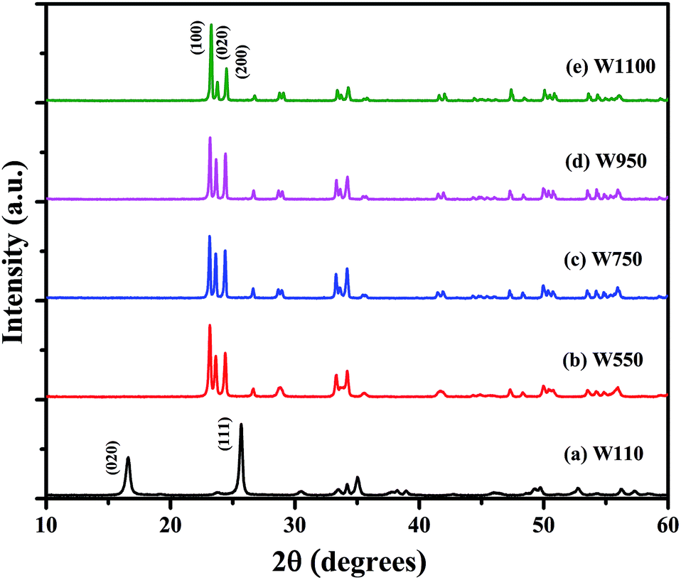 | ||
| Fig. 1 XRD pattern of (a) W110, (b) W550, (c) W750, (d) W950, (e) W1100 showing the phase transformation from orthorhombic phase (a) to monoclinic phase (b)–(e) and definite planes of growth with increase in annealing temperature. | ||
Absence of characteristic peaks corresponding to other impurities such as W or W(OH)6 indicates the phase purity of WO3 phase. The more separated and sharper peaks and higher number of reflections were observed in the XRD patterns of the WO3 annealed at higher temperature indicating an increase in degree of crystallinity with higher annealing temperature. This observation reveals that in the process of nanostructure formation definite planes of growth are affected by the varying temperature. The WO3 can exist in several polymorphic forms such as monoclinic, hexagonal and pyrochlore around room temperature. Choi et al. reported that sol prepared WO3 by ion exchange method contains both the hexagonal and pyrochlore phases which transform to the monoclinic phase on heating 500 °C and cooled down to room temperature.41 However, in the present study all the annealed samples exhibit only monoclinic WO3. A heat treatment leads to the removal of water molecules and formation of WO3 from WO3·H2O, as it is clearly evident from the changes in the XRD pattern shown in Fig. 1.
To verify the phase purity of the prepared samples, Rietveld refinement of all the samples was carried out using fullproof software as shown in Fig. 2. For sample W110, Rietveld refinement was done with WO3 orthorhombic phase having space group Pmnb. For samples W550, W750, W950 and W1100 the refinements were performed with WO3 monoclinic structure having space group P21/n. The refined lattice parameters are summarized in the Table 1. The reported parameters are in agreement with the earlier reported values.42 The observed Bragg's peaks of the diffractograms are characteristics of single phase WO3 in all the samples. Sample W110 contains single orthorhombic phase of tungstite while other samples W550, W750, W950 and W1100 contain single monoclinic phase structure of WO3. The reported lattice parameters do not show any significant lattice change which clearly indicates the absence of any additional crystalline phase or impurity.
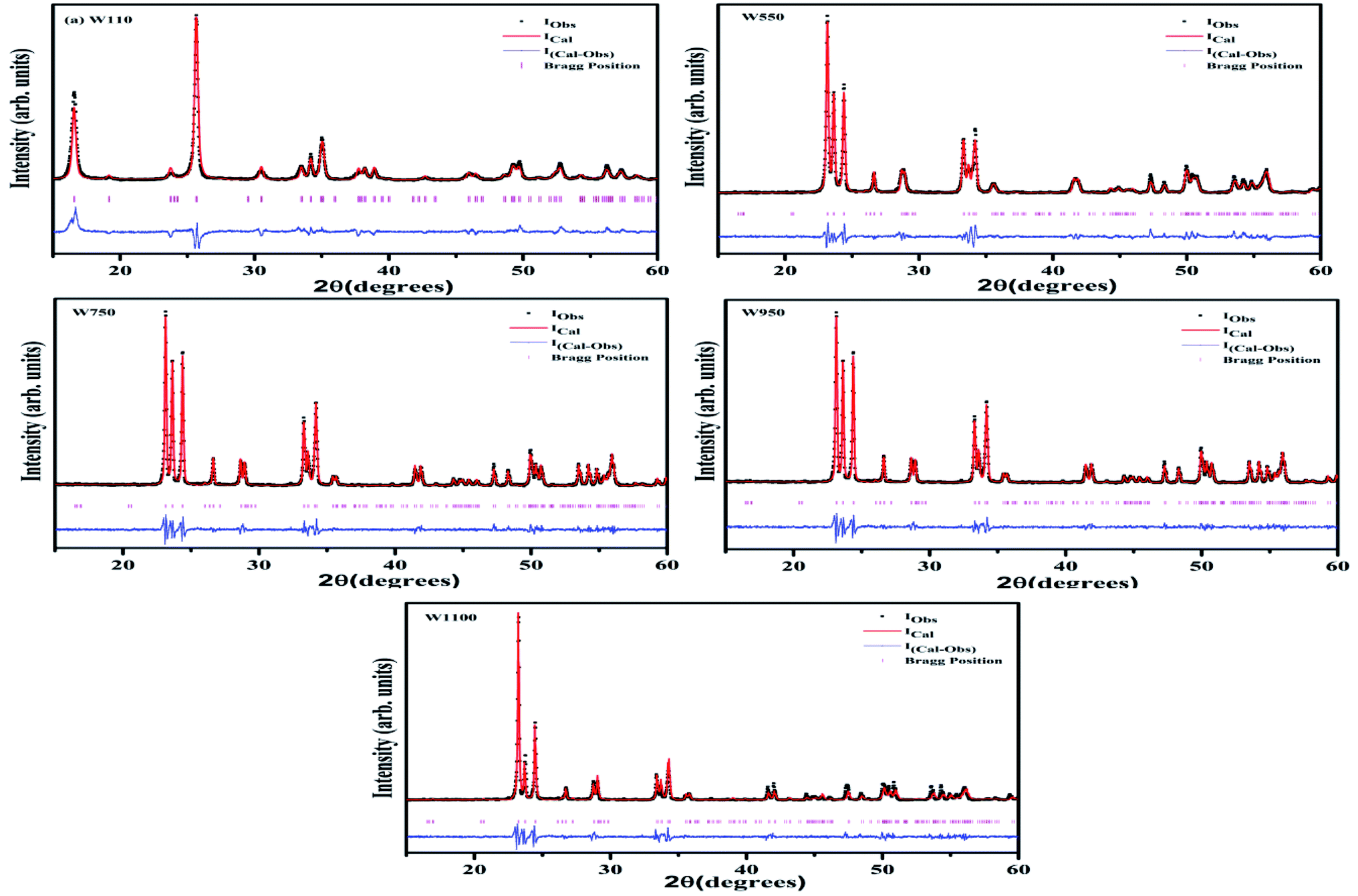 | ||
| Fig. 2 Rietveld analyses: observed and calculated XRD profiles of prepared samples. | ||
| Sample name | Lattice constants | Reliability factors | Goodness of fit (χ2) | ||||
|---|---|---|---|---|---|---|---|
| a/Å | b/Å | c/Å | Rp/% | Rwp/% | Rexp/% | ||
| W110 | 5.243 | 10.696 | 5.132 | 20.2 | 18.8 | 9.17 | 4.21 |
| W550 | 7.297 | 7.529 | 7.681 | 15.6 | 15.0 | 8.56 | 3.06 |
| W750 | 7.299 | 7.528 | 7.686 | 17.2 | 16.3 | 9.45 | 2.99 |
| W950 | 7.299 | 7.528 | 7.686 | 17.4 | 16.5 | 9.46 | 3.04 |
| W1100 | 7.297 | 7.528 | 7.680 | 16.9 | 16.4 | 8.46 | 3.75 |
XRD patterns show the broadening of peaks and are used to estimate the crystallite size (D) by Debye Scherrer's equation.43
 | (1) |
| βhkl2 = [βmeasured2 − βinstrumental2] | (2) |
The instrumental broadening was measured from the XRD pattern of standard material such as silicon. The values of the peak broadening were obtained by fitting of the major peaks i.e. (002), (120) and (200) for the WO3 (monoclinic) and (111) and (020) for the WO3·H2O (orthorhombic). The peaks become narrower i.e. the full width half maxima (FWHM) of samples decrease with increasing annealing temperature. The calculated crystallite size (D) and surface-to-volume ratio of the prepared samples at various annealing temperatures are shown in Table 2. As the particle size increases, the surface-to-volume ratio decreases. This behaviour is expected because the heating facilitates the diffusion and agglomeration of the particles. This can be attributed to the thermally promoted crystallite growth. The dislocation density (δ), which represents the amount of defects in the sample, is defined as the length of dislocation lines per unit volume of the crystal was also calculated and reported in Table 2.
| Sample name | Scherrer's D (nm) | Surface to volume ratio (nm−1) | Dislocation density × 10−3 (nm−2) | Williamson–Hall method | |
|---|---|---|---|---|---|
| D (nm) | Strain (ε) × 10−3 | ||||
| W110 | 25 | 0.04 | 1.60 | 29.57 | 0.69 |
| W550 | 34 | 0.03 | 0.87 | 49.18 | 0.42 |
| W750 | 48 | 0.020 | 0.043 | 53.7 | 0.43 |
| W950 | 56 | 0.017 | 0.032 | 60.33 | 0.36 |
| W1100 | 62 | 0.016 | 0.026 | 65.68 | 0.23 |
Along with the crystallite size, lattice strain also contributes to the broadening of the XRD peaks and has been estimated using the Williamsom–Hall (W–H) analysis. W–H analysis is a simplified integral breadth method used for estimating crystallite size and lattice strain, considering the broadening of peak as function of 2θ. On assuming that the particle size and strain contributions to X-ray line broadening are independent to each other, the observed line breadth can be given as
 | (3) |
On rearranging eqn (2), we get
 | (4) |
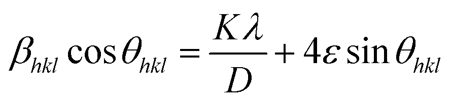
Eqn (3) is the W–H equation representing the uniform deformation model (UDM).45,46 In this model, crystal is considered as isotropic in nature and therefore it is assumed that the strain is uniform in all directions. The term (βhklcosθhkl) on y-axis was plotted as a function of (4sinθhkl) on x-axis as shown in Fig. 3 for the preferred orientation peaks of WO3 with orthorhombic and monoclinic structure. The strain (ε) and particle size (D) are represented by the slope and y intercept of the linearly fitted line. The values of D estimated using the W–H plot shows a similar trend to that obtained by Scherrer's equation and is tabulated in Table 2. The presence of O vacancies, structural imperfections and surface defects in WO3 nanoparticles can introduce micro-diffraction strain ε that results in the broadening of XRD peaks. It is found that the micro-diffraction strain for sample W110 has larger value which further decreases with increase in annealing temperature. This occurs because of defects like dislocations, edges or cuts. The oxygen vacancies are probably removed during annealing process. Thus, the microstrain ‘ε’ decreases and crystallite size ‘D’ increases with annealing temperature because of the decrease in surface defects and improved crystallinity due to higher annealing temperature.
 | ||
| Fig. 3 The W–H analysis of the prepared samples assuming UDM. Fit to the data, the strain is extracted from the slope and the crystalline size is extracted from the y-intercept of the fit. | ||
3.2 Scanning electron microscopy (SEM)
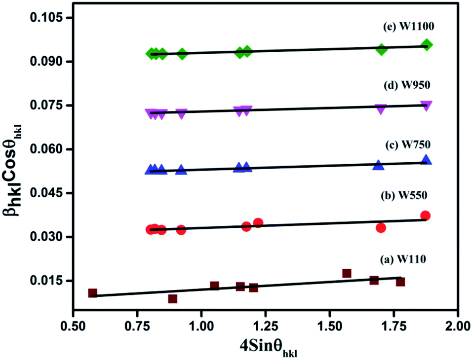
The surface morphology and composition of the samples were determined by SEM equipped with EDX analysis. Fig. 4(a–e) shows the SEM micrographs along with respective EDX patterns of W110, W550, W750, W950 and W1100. The images show that W110 has 2D layered nanosheets morphology with sharp edges and varying sizes grown in the direction of most intense (020) peak of the orthorhombic structure.1 The aggregation observed in the morphology of tungstite is due to the presence of water molecules which are connected to each other inside WO3 matrix with hydrogen bonds. On annealing the samples the water seems to be vaporized and removed from WO3 powders and hence the amount of aggregation is reduced. For W550 morphology has changed from nanosheets to nanoplatelets with soft edges grown along the intense (002) peak. For W750, well defined grain boundaries with cuboidal morphology having smooth surfaces are observed (Fig. 4(c)). Fig. 4(d) clearly shows the formation of more well defined 3D nano cuboids with larger grains as compared to the samples annealed at lower temperature.42 Due to thermal treatment the average grain size has increased by the diffusion of grain boundaries which resulted in the grain growth as observed from XRD results. It seems that at elevated temperatures, the high values of Gibb's energy favour agglomeration in a particular direction of most intense (002) peak of WO3 monoclinic structure, resulting into the change of morphology from nanocuboids to sea-rock like structure at 1100 °C.5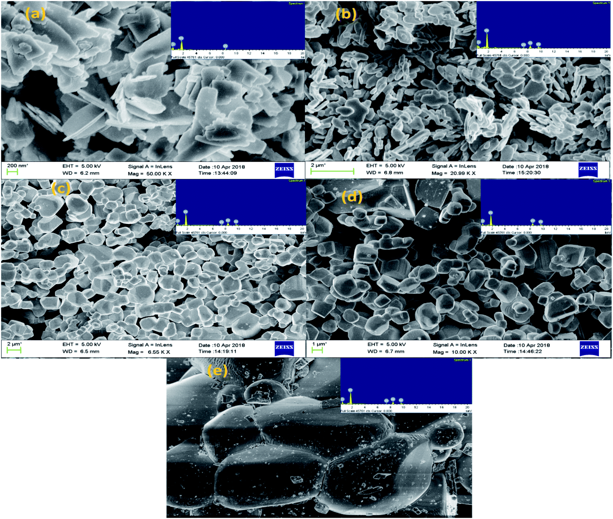 | ||
| Fig. 4 SEM images along with the EDX images in the inset for (a) W110, (b) W550, (c) W750, (d) W950, (e) W1100 sample. The figures clearly show the effect of annealing temperature on the surface morphology and grain size in the prepared samples. | ||
All the EDX patterns indicate W and O ions as the major elements with no remarkable impurities. Oxygen content is maximum in W110 sample due to additional O present in the form of water molecules. However, with phase transition from orthorhombic WO3·H2O to monoclinic WO3, the oxygen content has reduced considerably. With further annealing of the samples, the O content goes on increasing due to filling of O vacancies converting non-stoichiometric WO3−x into more stoichiometric WO3. Besides this, the hue of the WO3 powders also depends on the annealing temperature.44 The annealed powders W110, W550, W750, W950 and W1100 are yellow, light green, green, dark green and dark lustrous green in colour respectively.
3.3 Diffuse reflectance spectra (DRS)
Fig. 5 shows the diffused reflectance spectra of W110, W550, W750, W950, and W1100. A considerable red shift is observed in the absorption edge with increasing annealing temperature which indicates the decrease in band gap of WO3. The band gap energies (Eg) have been calculated using the Kubelka–Munk (K–M) model.47 | ||
| Fig. 5 Reflectance spectra of the annealed samples. Blue shift is observed in the sample W550 as compared to the sample W110. A red shift is observed in all the samples annealed above 500 °C due to increasing particle size with increasing annealing temperature. | ||
According to the K–M model at any given wavelength, F(R) = (1 − R)2/2R, where F(R) is the K–M function. A graph is plotted between [F(R)hν]n versus hν (Fig. 6), where n = 1/2 for indirect transitions, and the intercept value give the band gap energy Eg of the individual sample. The calculated band gap energies of all the annealed samples39 are tabulated in Table 3. These values are in agreement with the values reported in literature.46 Table 3 shows the decrease in band gap with the annealing temperature.
 | ||
| Fig. 6 Tauc plots indicating the indirect band gap for the corresponding reflectance spectra. The band gap energy is calculated from extrapolated (dashed) line fitted to respective linear portions in the graphs of the prepared samples. | ||
| Sample name | Band gap Eg/(eV) |
|---|---|
| W110 | 2.33 |
| W550 | 2.64 |
| W750 | 2.56 |
| W950 | 2.28 |
| W1100 | 2.13 |
It is generally agreed that the top of the valence band arises from O 2p states and the bottom of the conduction band is mainly W 5d states with some mixing with O 2p states.4–9,49 The band gap is a sensitive function of W–O bond length. Therefore, in WO3 containing O vacancies there is a structural relaxation resulting in an increase of W–W distance due to Coulomb repulsion and change in W–O splitting. Consequently, the band gap increases which are consistent with the experimental observations that in samples W550, W750 with more oxygen vacancies, the band gap is significantly larger as compared to the samples W950 and W1100. The structural distortions in WO6 octahedra can lead to the displacement of W-ion from the center of the octahedron. This off-centring results in lowering of the valence band and raising the conduction band with a consequent increase in the band gap as the structure changes from more symmetric WO3·H2O orthorhombic to less symmetric WO3 monoclinic. The decrease in the band gap values can also be ascribed to the increasing crystallite growth with increasing annealing temperature.
3.4 Raman studies
In order to investigate the effect of annealing temperature on the vibrational properties of WO3 nanostructures, a Raman scattering study has been performed on the prepared samples (Fig. 7). For the sample W110, the peaks at 638 cm−1 and 946 cm−1 are assigned to the ag phonons of the WO3·H2O lattice, in agreement with previous reports.48 These two peaks are associated with the stretching mode of the W(6+)–O(2) and W(6+)–O(3) respectively. For Tungstite, the W![[double bond, length as m-dash]](https://www.rsc.org/images/entities/char_e001.gif) O bond peak, is caused by structural water molecules. One of the axial O positions in the octahedron can be occupied by a structural water molecules and this O is associated with a single bond and the opposite axial O forms a strong WO double bond. These two O bonds are associated with the 638 cm−1 and 946 cm−1 respectively are characteristic peaks of orthorhombic WO3·H2O. The bond length of band at 638 cm−1 is larger than that of band at 946 cm−1; hence the former appears at lower frequency than latter. Two smaller peaks in the range 180–250 cm−1 are assigned to the bonding or the deformation of O–W–O bonds in WO3·H2O.48
O bond peak, is caused by structural water molecules. One of the axial O positions in the octahedron can be occupied by a structural water molecules and this O is associated with a single bond and the opposite axial O forms a strong WO double bond. These two O bonds are associated with the 638 cm−1 and 946 cm−1 respectively are characteristic peaks of orthorhombic WO3·H2O. The bond length of band at 638 cm−1 is larger than that of band at 946 cm−1; hence the former appears at lower frequency than latter. Two smaller peaks in the range 180–250 cm−1 are assigned to the bonding or the deformation of O–W–O bonds in WO3·H2O.48
 | ||
| Fig. 7 Raman spectra for different annealed samples (a) W110, (b) W550, (c) W750, (d) W950, and (e) W1100. The characteristic Raman modes of WO3 are indicated in each case. The peak positions marked with arrows in (a) show orthorhombic phase of WO3·H2O. | ||
The Raman spectra of the samples W550, W750, W950, W1100, are quite similar which clearly indicate that WO3 does not change the crystalline phase with the annealing temperature above 500 °C. The intense peaks centred at 807cm−1and 719 cm−1 are the typical Raman peaks of the crystalline monoclinic WO3 (m-phase) that corresponds to the stretching vibrations of the bridging oxygen ν (O–W–O).39 The sharp peaks at 274 cm−1 and 329 cm−1 are assigned to the bending vibrations of δ (O–W–O) bond. In the low wave number regions, the band at 36 cm−1 can be assigned to the existence of WO3 grains in monoclinic phase. However, the peaks observed in the region 50–100 cm−1 are ascribed to the lattice vibrations of both WO3·H2O and monoclinic WO3.
3.5 Photoluminescence
The PL studies of the materials help to understand the presence of various defects, impurities and energy states available within the conduction band and valence band of the material. Karazhanov et al. studied the oxygen vacancies in cubic WO3 by using the first principle pseudo-potential calculations.52 Their theoretical findings show that oxygen vacancies in WO3 give rise to 3 types of defect states, a donor like state within the fundamental band gap, a hyper deep resonant state in the valence band and a high lying resonant state in the conduction band. According to these studies, the NUV emission is ascribed to the recombination between the electron occupying the resonant defect state in conduction band and a hole in the valence band. Such an electron–hole pair forms a Frenkel exciton bound nearby an oxygen vacancy.53 Once an electron is excited to the states at or above a resonant level, it is probable to be trapped by the resonant state. If the electrons are excited to the higher states above resonant level, then there is larger probability of an electron to get trap at resonant levels. This explains the strong dependency of the NUV emission at the excitation wavelength.The PL measurements were performed for all the synthesized samples at room temperature. The samples were excited by light at wavelengths 250 nm, 320 nm and 450 nm. At λexc = 250 nm (4.96 eV), the electrons are excited to the highest unoccupied energy levels between eg and t2g levels which can be supported from the fact that crystal field splitting energy of t2g and eg levels is 5.26 eV.20 The similar energy gap between t2g and eg levels has been recorded through XAS studies (Fig. 16) in the later section of the paper. In the emission spectra recorded at excitation wavelength 250 nm (Fig. 8), two emission peaks at 293 nm and 397 nm are observed in the NUV region.49,50 These NUV emissions are attributed to the localized resonant states of the O vacancies in the conduction band of the prepared samples. Luo et al. attributed the NUV emission centred at 395 nm due to the states of oxygen vacancies in the conduction band of WO3−x nanowire networks.51 At λexc = 320 nm, the PL spectrum shows four peaks at 386 nm, 463 nm, 478 nm, and 527 nm (Fig. 9). The emission at 386 nm corresponds to NUV emission. The blue shift is observed in the peaks of sample W550 as compared to sample W110, which is usually caused by band structure deformation resulting from lattice disorder as the phase of WO3 changes from orthorhombic to monoclinic.54 The blue emission at 463 nm (2.68 eV) agrees with the value of 2.6–2.7 eV for the indirect band gap of monoclinic WO3 suggesting that the blue emission is due to band to band transition.45 In the Fig. 10, the samples excited at 450 nm give single emission peak at 623 nm. As shown in Fig. 9 and 10 respectively, the emissions observed at 478 nm, 527 nm (λexc = 320 nm) and 623 nm (λexc = 450 nm) can be explained as optical transitions due to oxygen vacancy states (neutral V0O, singly charged VO1+, doubly charged VO2+) lying below the conduction band minimum within the fundamental band gap. The recorded values are in accordance with the previously reported values in the literature.5,55,56 The reduction in emission intensity is observed in sample W550 as compared to sample W110 due to structural phase transformation as observed in XRD, Raman and XAS studies. While the further reduction in intensity in the samples W750, W950 and W1100 (as observed in Fig. 8, 9 and 10) is due to the filling up of oxygen vacancies and removal of defects with increase in annealing temperature. As the annealing temperature of WO3 nanostructures increases up to 1100 °C, the crystallite size becomes larger and the crystallinity becomes better, while the intensity of the oxygen vacancies related luminescence peaks (478 nm and 560 nm) is found to decrease. With the increase in annealing temperature up to 500 °C, the concentration of surface oxygen increases and the further increase in annealing temperature is accompanied by a decrease in oxygen vacancies, while the relevant crystalline performance is enhanced by a decrease in bulk defects. Such a decrease in NUV emission intensity observed in samples due to decrease in oxygen vacancies also suggests the formation of more stoichiometric WO3. The decrease in PL intensity in other peaks except NUV is observed due to change in morphology of the WO3 nanostructures from 2D-nanosheets to 3D-nanocuboids. By combining the PL results with SEM analysis, it is observed that with increase in annealing temperature, the average particle size has increased in samples, in other words, the surface-to-volume ratio of the nanostructures decreases leading to longer mean free path of electron motion which accounts for lower emission intensity.58 Therefore, the emission peaks at 478, 527 and 623 nm show decrease in the emission intensity. Also, the shift observed in the position of emission bands, as we move from sample W550 to W1100, could be resulted due to the change of strain in the samples because of lattice distortions and relaxations on annealing the samples.
 | ||
| Fig. 8 PL spectra of the annealed samples recorded at λexc = 250 nm showing the emissions in NUV region due to presence of different resonant vacancy states in conduction band. | ||
 | ||
| Fig. 9 PL spectra of the annealed samples recorded at λexc = 320 nm giving emission at 386 nm due to resonant states in the CB; emission at 463 nm due to band–band transition and emission peaks at 478 nm and 527 nm due to donor like states present within band gap. | ||
 | ||
| Fig. 10 PL spectra of the annealed samples recorded at λexc = 450 nm. The emission is due to optical transition from different oxygen vacancy states (VO2+/VO1+). | ||
To explore further the different charged states of oxygen vacancies responsible for emission peaks; we tried to get better insight into the influence of crystal structure over oxygen vacancies inside WO3 matrix. As a result of pseudo-Jahn–Teller distortion in monoclinic WO3, the axes are tilted relative to each other and the central W atom exhibits an off-centring displacement along the three crystallographic directions a, b and c.57 Due to such distortion, the band gap drastically increases as one moves from most symmetric cubic phase to monoclinic structures. Such transitions cause the change in the hybridization properties of valence band (VB) and conduction band (CB) edges as a result of W–O bond length splitting and tilting of the octahedron. This structural anisotropy as observed in the XAS spectra (Fig. 16) reflects the different behaviours of the oxygen vacancies depending on the direction of the W–O–W chain where these are created. Thus, the emission properties are also expected to be affected by such anisotropy. The oxygen vacancies oriented on crystallographic axes ‘a’ tend to form colour centers configurations with the excess charge localized in the vacancy void to yield a closed shell singlet ground state.
On the other hand, oxygen vacancies oriented along the b and c axes give rise to polaronic defect centers due to strong lattice relaxations occurring along the defective W–O–W chain. The excess charge primarily localizes on the 5d orbitals of the W atoms along the chain, yielding a neutral vacancy, an open shell triplet ground state.20 Thus, the obtained PL spectra exhibit several peaks, which can be explained in light of above said theory. The emission at 527 nm (Fig. 9) can be explained due to (VO2+/VO1+) vertical transitions involving oxygen vacancies along crystallographic axes b and c, while the emission at 623 nm (Fig. 10) is due to (VO2+/VO1+) optical transitions involving oxygen vacancies along the crystallographic axes ‘a’.20 In this case, an excited electron from the CB is initially trapped at doubly charged (VO2+) oxygen site to form a singly charged (VO1+) oxygen vacancy and then simultaneous recombination of defect electron with hole in the VB would lead to emission of photons with energies 2.3 and 1.99 eV along their respective axes.
On the same background, the peak at 478 nm (Fig. 9) is expected to arise due to (VO2+/V0O) vertical transition along crystallographic axes b and c. All these observations suggest that the emissions are related to electron–hole recombination involving the valence band and midgap donor like oxygen vacancies defect level. The band diagram of WO3, including recombination between different states leading to strong visible luminescence and NUV emissions due to high lying resonant oxygen vacancies states, is illustrated in Fig. 11.
 | ||
| Fig. 11 Band diagram of WO3 showing NUV emissions (293 nm, 397 nm, and 386 nm) due to resonant states of oxygen vacancies, band to band transition (463 nm), emission due to midgap defect states along (+2/0) transition along crystallographic axes b and c (478 nm), along (+2/+1) transition along crystallographic axes b, c (527 nm) and axes a (623 nm). | ||
The overall emitted colours have been characterized with the help of Commission International De I'Eclairage (CIE) chromaticity coordinates, where any colour can be expressed in terms of (x, y) colour coordinates. The colour coordinates evaluated for the prepared samples under excitation at 250 nm, 320 nm and 450 nm are shown in Fig. 12. With the change of excitation wavelength, the light emitted from the prepared samples shows shift from violet to red region. So, prepared samples can be tuned and controlled for various lighting applications.
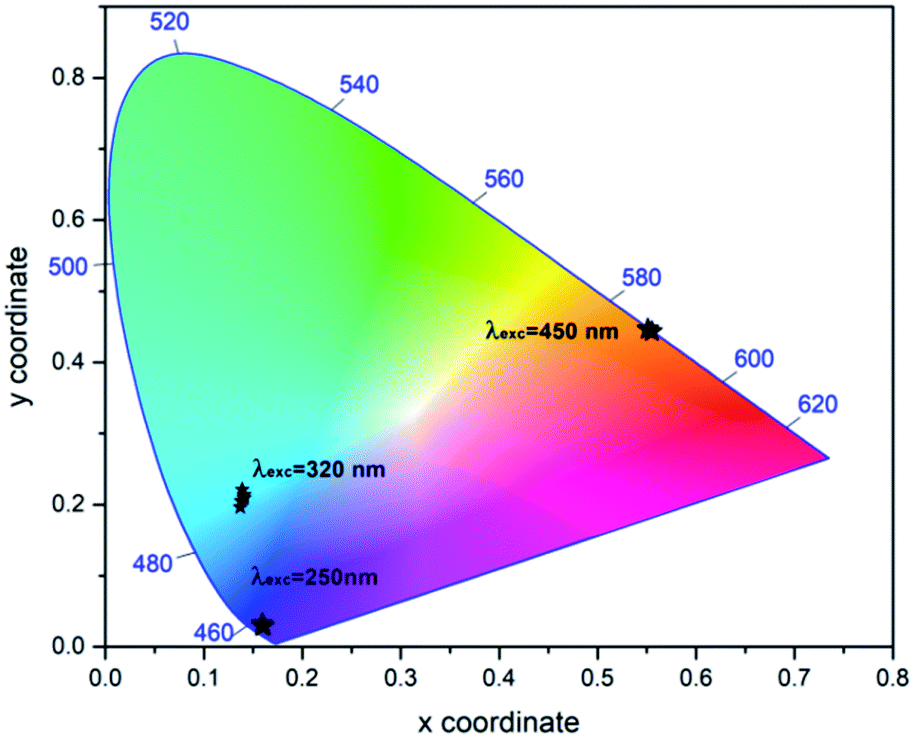 | ||
| Fig. 12 Spectral chromaticity colour coordinate diagram. | ||
3.6 Magnetic studies
Magnetization loops for the as dried and annealed samples were measured at 300 K using a VSM magnetometer and the M–H curves are shown in Fig. 13. The actual magnetization of the samples was determined after subtraction of the diamagnetic background. It is observed that all the samples exhibit a clear hysteresis loop, indicating that these nanostructures are ferromagnetic in nature59 with Curie temperature > 300 K. The curves for all the samples clearly show the typical ferromagnetic saturation behaviour. From Fig. 13 it is clearly seen that the sample W110 having orthorhombic phase has highest value of Ms (0.005 emu g−1). Thiyagarajan et al. have reported a maximum Ms of 0.009 emu g−1 in undoped WO3 nanorods.60 The appreciable decrease in Ms value (0.0013 emu g−1) is observed for the monoclinic sample. It is well known that the magnetic properties of the materials are very sensitive to change of the underlying electronic structure and the band structure which are further dependent on the crystal structure. Therefore, such decrease could have occurred due to phase transition from orthorhombic to monoclinic which leads to variation in splitting of the eg and t2g orbitals of the conduction band of tungsten ion.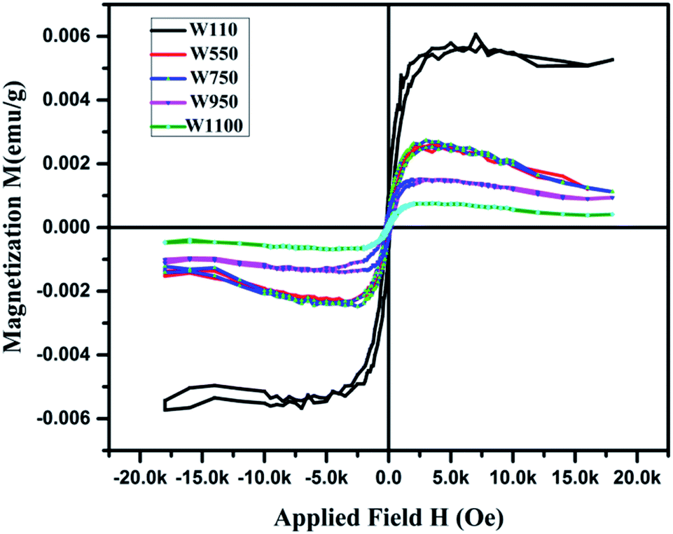 | ||
| Fig. 13 Typical hysteresis loops of the annealed samples at 300 K. | ||
For samples W750, W950 and W1100, Ms decreases with increasing annealing temperature. It clearly points out that the FM in WO3 nanostructures is intrinsic and defect mediated. Decrease in magnetic moment has been observed in the samples annealed above 500 °C which proves the fact that the magnetism in WO3 originates from oxygen vacancies.61 Filling up of oxygen vacancies enormously degrades the magnetic ordering of these compounds.62,63 Nguyen Hoa Hong also reported the assumption that magnetism in HfO2 thin films originates from defects and/or oxygen vacancies.64 We further tried to explore the connection between the structural changes and magnetization for all these samples. From the XRD results, it is clearly evident that the annealing at higher temperature causes a monotonic increase of the crystallite size (D) of the samples. Thus, if one plots the MS vs. 1/D, the variation is more or less linear (Fig. 14). The parameter 1/D can be taken as proportional to the grain surface to volume ratio.
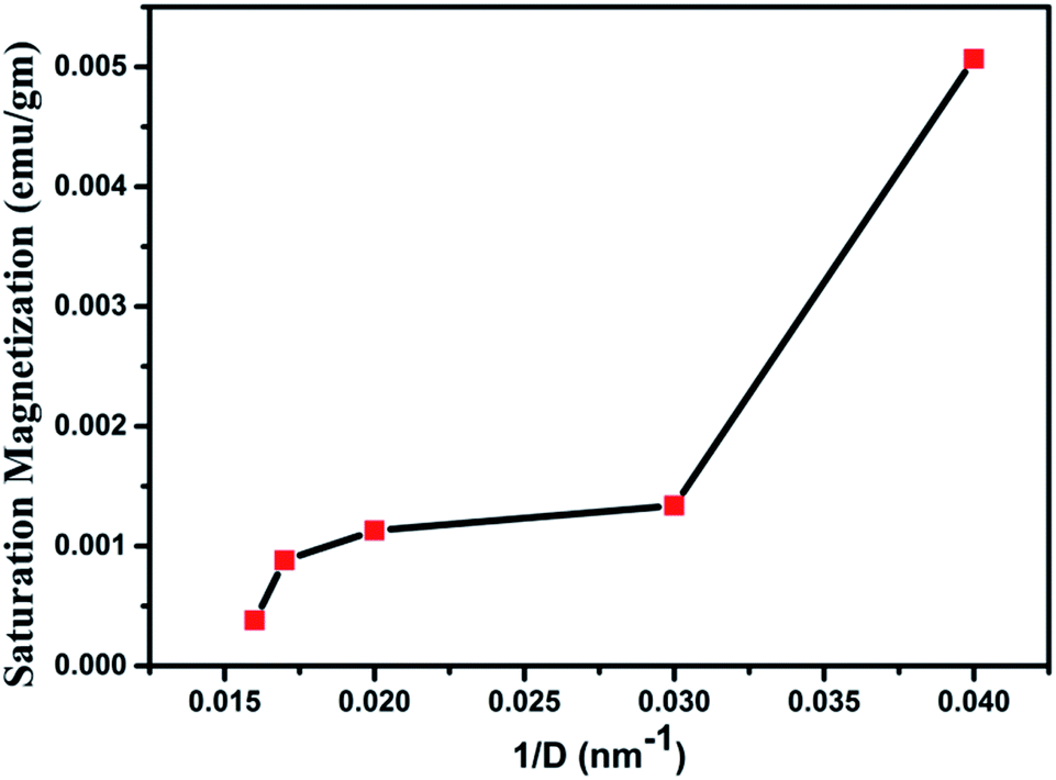 | ||
| Fig. 14 Variation of saturation magnetization with inverse of average grain size for WO3 samples. | ||
In fact, this increasing trend of Ms with 1/D agrees with the previous reported trends in the literature. Such trend clearly indicates that FM in WO3 is indeed a grain surface related phenomenon besides the presence of defects present in the system.65 Fig. 15 illustrates the variation of Ms and coercivity (Hc) with annealing temperature. Below 500 °C both the parameters decrease with increase in annealing temperature. This could be due to change in phase transformation from orthorhombic to monoclinic structure. Above 500 °C, the variations of Ms and Hc with annealing temperature exhibit opposite nature. This behaviour is a typical of a soft ferromagnet.66 However, above 950 °C both parameters decrease with increasing annealing temperature. Such observation reveals that Ms and Hc are related to not only the grain size of the samples as occurred for ordinary ferromagnetic materials but also to the intrinsic defects present inside the sample and at the grain boundaries. Such a decrease may be due to the expected cross over from the single domain to multi-domain nature in the sample with increase in annealing temperature.
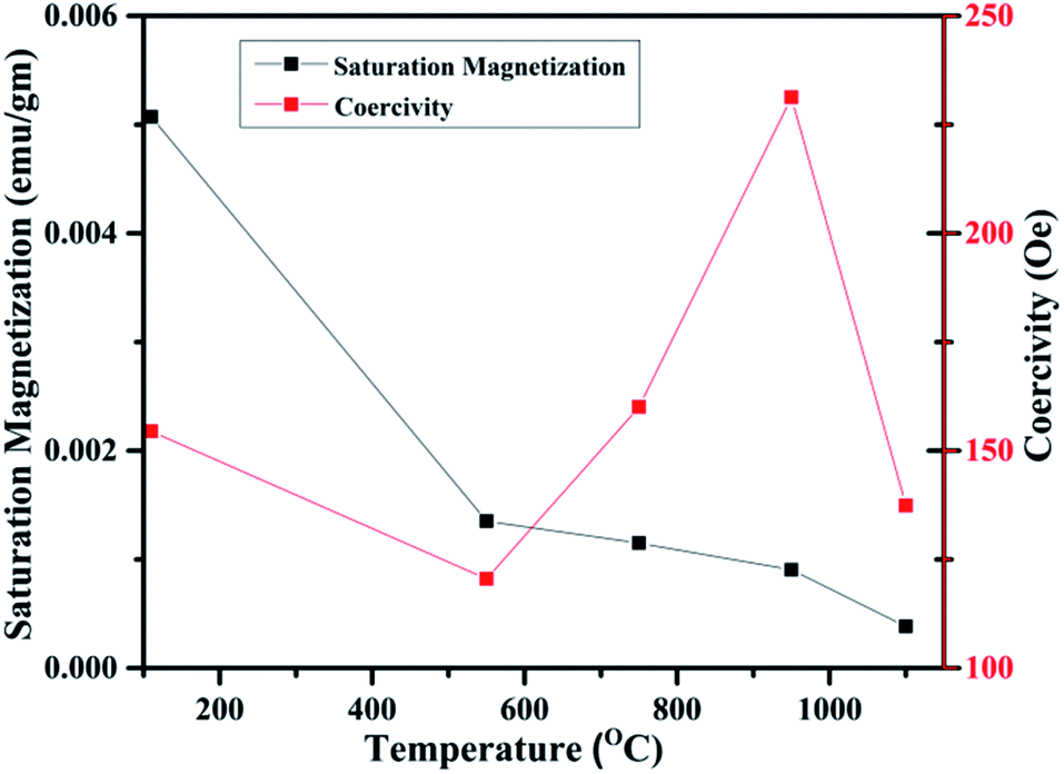 | ||
| Fig. 15 Variation of saturation magnetization and coercivity with temperature. | ||
3.7 XAS studies
The normalized spectra of O–K edge studies are shown in Fig. 16. The origin of the first peak is related to the unoccupied states at the bottom of the conduction band. The first absorption peak (A, B) with maximum intensity consists of the main peak A and the shoulder B. This peak arises from the O 2p and W 5d anti bonding states of local symmetry48 i.e. due to 5d(t2g)–2p(O)67 interaction. Since the pre-peak of O K-edge of WO3 is originated from the strong hybridization between O 2p and W 5d orbitals, any change of the pre-peak reflects the change of 5d occupancy, which may be associated with the oxygen vacancy. As per the dipole selection rules, O K-edge spectra provide information about the transitions involved from O 1s to unoccupied bound and free states with p-character which are relaxed in the presence of the 1s core hole +ve charge. Due to hybridization between metal d and oxygen 2p orbitals, we can gather some information about the shape of density of metal d-states from the O K-edge spectra. The shoulder B reflects the anisotropy of the d(t2g) band presented in the non-cubic perovskites such as m-WO3 and WO3·H2O. Such anisotropy results due to presence of non-equivalent Oxygen atoms of the first co-ordination shell. The amount of the TM–O bond covalency and the occupancy of the conduction band determine the number of 2p(O) empty states. The peak intensity of A and B determines the number of 2p(O) empty states. Therefore, from Fig. 16, it is clearly seen that the intensity of the peak A increases for the sample W110, W550 to W750 and decreases for the W950 to W1100. Therefore, it is expected that the samples become more covalent with increase in annealing temperature up to 750 °C and further the covalent character decreases with rise in temperature from 950 °C to 1100 °C which is expected due to increasing particle size and changing morphology of the nanoparticles. Moreover, the FWHM of the peak is related to the width of the d(t2g) band.
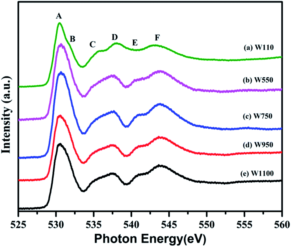 | ||
| Fig. 16 O–K edge fine structure of prepared samples (a) W110, (b) W550, (c) W750, (d) W950 and (e) W1100. Disappearance of peaks B and C in spectra (b)–(e) reflects the change in hybridization between O 2p and W 5d orbitals with structural phase transformation. | ||
The intensity of the first peak at 530.50 eV increases significantly from WO3·H2O to W750 and decreases from W950 to W1100. A similar trend is observed in broadening as we move from sample W110 to W1100 which suggests that crystal symmetry initially decreases from orthorhombic WO3·H2O to monoclinic WO3 but with increase in temperature the symmetry improves with the decrease in strain and increase in particle size. The area of the first peak is greatly influenced by the W–O bond covalency. Therefore, sample W750 is considered to have the strong covalent W–O bonds. The splitting of the first peak A (Fig. 16) in distorted perovskites (WO3·H2O) is prominently seen due to presence of several non-equivalent oxygen atoms.68 WO3·H2O, being a layered compound as observed in SEM results (Fig. 4(a)), has two main contributions from the intralayer and interlayer oxygen atoms, giving rise to two peaks A and B respectively. Due to the absence of oxygen atoms of the interlayer water molecule in m-WO3, the peak becomes less prominent and eventually vanishes with increase in annealing temperature. The peaks C and D result due to 5d(eg)(W)–2p(O) hybridization which is strongly influenced by the distortion of the WO6 octahedra.67,68 Increase in intensity of peak C and peak D in the annealed samples at low temperature suggests partially covalent interaction between oxygen and metal ions which eventually decreases in samples annealed at higher temperature. The difference between the A and C peaks gives the rough estimate of the splitting between the t2g and eg sub bands in tungsten oxide. This energy difference between t2g and eg orbitals for all the samples is found to be in the range 5.048–5.312 eV which is comparable to the theoretical estimate 5.5 eV for cubic WO3.20 The peaks E and F are attributed to 6sp(W)–2p(O) interaction and their variations have similar behaviour as that of peaks C and D.
Above results clearly show the presence of oxygen vacancies associated with interesting optical properties and the observation of FM in thermally annealed nanostructured WO3.
Of the models available to understand these oxides, Bound Magnetic Polaron (BMP) model is commonly used. In this model, the oxygen vacancy as defect mediates the spins of localized electrons of dopant ions in their d orbitals.69 But the mechanism of FM in pure WO3 without magnetic ions is still debatable. Here, we give simple approach; a large concentration of oxygen vacancy defects is observed in the prepared samples from the PL spectrum. It is supposed that the possible origin of the FM in WO3 nanoparticles is through F-centre exchange (FCE), which is a sub-category of the BMP model. The concept of the FCE coupling is based on the BMP model and is interpreted with reference to the presence of oxygen vacancies; the magnetic ions via vacancies (F-center) constitute a BMP and produce FM.70 The WO3 nanostructures have comparable octahedral W–O bonds where each W atom has 6 neighbouring O atom. With the removal of an oxygen atom, the two electrons are left behind in reduced WO3 which may form three kind of oxygen vacancy related colour centers such as oxygen vacancy with doubly occupied electrons V0O (F-center with two electrons), singly ionized oxygen vacancy VO1+ (F+ center with one electron) and doubly ionized oxygen vacancy VO2+ (F++center with no electron). However, the F and F++ centers have spin-zero ground states; thus, they do not induce FM in WO3. It is known that the F+ centers are paramagnetic and can activate BMPs in WO3. Direct exchange among these BMPs leads to the formation of ferromagnetic domains. As a consequence, it might be assumed that the singly occupied oxygen vacancies (i.e., the F+ centers) possibly induce the FM in WO3 nanoparticles which also coincides with some previously reported results. Coey et al. reported that F centers with two electrons form 1s2 state, which give rise to weak antiferromagnetic exchange.71 Da Pieve et al. reported that F++centers would not favour FM in TiO2 based systems.72 Thus, F+ centers seems to be a main carrier for the origin of FM. Apart from this, the localization of the excess electrons takes place on the 5d orbitals of the W6+cations of WO3. As a result there will be formation of mixed W6+, W5+ and W4+ states in the nanoparticles.20 Moreover, two W5+ ions seem to induce an equal and opposite local magnetic moment at neighbouring oxygen vacancies which would result in net anti FM. Therefore, the FM might consequently arise from a nearest neighbour interaction double exchange (W5+–O–W6+), (W5+–O–W4+), or superexchange (W5+–O–W5+) both of which are mediated by oxygen vacancies via F center exchange.
To further verify this, the defect analysis using PL studies also show the presence of singly occupied oxygen vacancies. The emission at 527 nm (Fig. 9) and 623 nm (Fig. 10) in the PL spectra is due to transitions involving singly charged oxygen vacancies. The PL intensity and magnetic parameters decrease gradually with increase in the annealing temperature and eventually for the samples annealed at 1100 °C a weak FM is observed. This is directly related to the decrease in concentration of singly ionized oxygen vacancy VO1+ and increase in size of the nanoparticles.73
Aljawfi et al. reported the similar results where the FM in the pure ZnO may be correlated with the change in the net number of electrons in the 3d state of Zn induced by VO.69
4 Conclusions
In summary, we have synthesized the pure WO3 nanostructures through acid precipitation method and annealed at various temperatures. The structure and morphology are studied by XRD and SEM. XRD confirms the phase transformation from tungstite to tungsten oxide with increase in annealing temperature and formation of crystalline monoclinic lattice structure at or above 500 °C. The crystallite size calculated from Scherrer's formula agrees with that obtained from W–H plot analysis. The UV-DRS studies exhibit a decrease in band gap of annealed WO3 nanostructures attributed to the structural distortions and increased crystallite growth. Micro-Raman spectra also reflect the phase transition from orthorhombic WO3·H2O to monoclinic WO3 without any further change in crystal structure with annealing temperature.PL studies conclude the presence of defects states (O vacancies along different crystallographic axes) in the samples which has shown decrease with increasing annealing temperature as indicated by the decrease in the intensity of emission bands. The spectral chromaticity colour coordinates indicate the wavelength dependent visible emission from violet to red region in the prepared samples making them promising candidates for use in optical displays. We have observed the room temperature FM in undoped WO3 nanostructures which is otherwise diamagnetic in nature. Since there is no sign of impurity observed from XRD and Raman studies, we found that oxygen vacancies VO are mainly responsible for dictating the magnitude of FM in these samples. By comparing the oxygen vacancy VO related visible emissions from PL spectra and saturation magnetization from M–H loops, the observed room temperature FM is explained on the basis of BMPs whose formation is due to the F center exchange interaction between different tungsten ions in the vicinity of VO. The value of saturation magnetization decreases with increase in the annealing temperature. XAS studies reflect the variations in the local electronic structure and covalent character of the nanostructured WO3 with annealing temperature. Above studies show that the colour tunability can be achieved in WO3 based systems by exciting the material at different wavelengths while the magnetization values can be tuned by changing the relative concentration of oxygen vacancies that can be further achieved by varying the annealing temperature.
Conflicts of interest
There are no conflicts to declare.Acknowledgements
Authors thank Dr C. L. Dong, Department of Physics, Tamkang University, Taiwan for research discussion and XAS measurements.References
- S.-Q. Guo, M.-M. Zhen, M.-Q. Sun, X. Zhang, Ya-P. Zhao and L. Liu, RSC Adv., 2015, 5, 16376–16385 RSC.
- S. Wang, S. V. Kershaw, G. Li, K. Michael and H. Leung, J. Mater. Chem. C, 2015, 3, 3280 RSC.
- M. A. Butler, J. Appl. Phys., 1977, 48, 1914–1920 CrossRef CAS.
- C. G. Granqvist, Sol. Energy Mater. Sol. Cells, 2000, 60, 201–262 CrossRef CAS.
- B. Ahmed, S. Kumar, A. K. Ojha, P. Donfack and A. Materny, Spectrochim. Acta, Part A, 2017, 175, 250–261 CrossRef CAS PubMed.
- P. P. González-Borrero, F. Sato, A. N. Medina, M. L. Baesso, A. C. Bento, G. Baldissera, C. Persson, G. A. Niklasson, C. G. Granqvist and A. Ferreira da Silva, Appl. Phys. Lett., 2010, 96, 061909 CrossRef.
- B. Marsen, B. Cole and E. L. Miller, Sol. Energy Mater. Sol. Cells, 2007, 91, 1954–1958 CrossRef CAS.
- G. Hodes, D. Cahen and J. Manassen, Nature, 1976, 260, 312–313 CrossRef CAS.
- F. Di Quarto, A. Di Paulo and C. Sunseri, Electrochim. Acta, 1981, 26, 1177–1184 CrossRef CAS.
- T. Siciliano, A. Tepore, G. Micocci, A. Serra, D. Manno and E. Filippo, Sens. Actuators, B, 2008, 133, 321–326 CrossRef CAS.
- B. Ahmed, A. K. Ojha, F. Hirsch, I. Fischer, D. Patrice and A. Materny, RSC Adv., 2017, 7, 13985 RSC.
- C. O. Avellaneda and L. O. S. Bulhoes, Solid State Ionics, 2003, 165, 117–121 CrossRef CAS.
- W. Jing, X. Jiao, T. Wang and D. Chen, J. Mater. Chem. C, 2015, 3, 7597–7603 RSC.
- X. Zeng, Y. Zhou, S. Ji, H. Luo, H. Yao, X. Huang and P. Jin, J. Mater. Chem. C, 2015, 3, 8050–8060 RSC.
- C. Pedro, V. Rico-Gavira, C. Lopez-Santos, A. Barranco, V. Perez-Dieste, C. Escudero, J. P. Espinos and A. R. Gonzalez-Elipe, J. Phys. Chem. C, 2017, 121, 15719–15727 CrossRef.
- B. Ahmed, A. K. Ojha, A. Singh, F. Hirsch, I. Fischer, D. Patrice and A. Materny, J. Hazard. Mater., 2018, 347, 266–278 CrossRef CAS PubMed.
- R. Chatten, A. V. Chadwick, A. Rougier and P. J. D. Lindan, J. Phys. Chem. B, 2005, 109, 3146–3156 CrossRef CAS PubMed.
- P. M. Woodward, A. W. Sleight and T. Vogt, J. Phys. Chem. Solids, 1995, 56, 1305–1315 CrossRef CAS.
- F. Wang, C. Di Valentin and G. Pacchioni, Phys. Rev. B: Condens. Matter Mater. Phys., 2011, 84, 073103 CrossRef.
- M. Gerosa, C. Di Valentin, G. Onida, C. E. Bottani and G. Pacchioni, J. Phys. Chem. C, 2016, 120, 11716–11726 CrossRef CAS.
- C. V. Ramana, S. Utsunomiya, R. C. Ewing, C. M. Julien and U. Becker, J. Phys. Chem. B, 2006, 110, 10430–10435 CrossRef CAS PubMed.
- R. S. Vemuri, K. Kamala Bharathi, S. K. Gullapalli and C. V. Ramana, ACS Appl. Mater. Interfaces, 2010, 2, 2623–2628 CrossRef CAS PubMed.
- M. Niederberger, M. H. Bartl and G. D. Stucky, J. Am. Chem. Soc., 2002, 124, 13642–13643 CrossRef CAS PubMed.
- K. Lee, W. S. Seo and J. T. Park, J. Am. Chem. Soc., 2003, 125, 3408–3409 CrossRef CAS PubMed.
- M. Feng, A. L. Pan, H. R. Zhang, Z. A. Li, F. Liu, H. W. Liu, D. X. Shi, B. S. Zou and H. J. Gao, Appl. Phys. Lett., 2005, 86, 141901 CrossRef.
- M. Manfredi, C. Paracchini, G. C. Salviati and G. Schianchi, Thin Solid Films, 1981, 79, 161–166 CrossRef CAS.
- J. Eervenka, M. I. Katsnelson and C. F. J. Flipse, Nat. Phys., 2009, 5, 840 Search PubMed.
- J. Hong, J. Appl. Phys., 2008, 103, 063907 CrossRef.
- M. Khalid, M. Ziese, A. Setzer, P. Esquinazi, M. Lorenz, H. Hochmuth, M. Grundmann, D. Spemann, T. Butz, G. Brauer, W. Anwand, G. Fischer, W. A. Adeagbo, W. Hergert and A. Ernst, Phys. Rev. B: Condens. Matter Mater. Phys., 2009, 80, 035331 CrossRef.
- N. H. Hong, J. Sakai, N. Poirot and V. Brize, Phys. Rev. B: Condens. Matter Mater. Phys., 2006, 73, 132404 CrossRef.
- P. Z. Si, C. J. Choi, E. Bruck, J. C. P. Klaasse, D. Y. Geng and Z. D. Zhang, Phys. B, 2007, 392, 154–158 CrossRef CAS.
- V. Hariharan, V. Aroulmoji, K. Prabakaran, B. Gnanavel, M. Parthibavarman, R. Sathyapriya and M. Kanagaraj, J. Alloys Compd., 2016, 689, 41–47 CrossRef CAS.
- G. Baldissera and C. Person, Eur. Phys. J., 2013, 86, 273 Search PubMed.
- T. Inoue, K. Ohtsuka, Y. Yoshida, Y. Matsuura and Y. Kajiyama, Sens. Actuators, B, 1995, 24–25, 388–391 CrossRef.
- J. J. Shieh, H. M. Feng, M. H. Hon and H. Y. Juang, Sens. Actuators, B, 2002, 86, 75–80 CrossRef CAS.
- M. Akiyama, J. Tamaki, N. Miura and N. Yamazoe, Chem. Lett., 1991, 273, 1611–1614 CrossRef.
- Z. Lu, S. M. Kanan and C. P. Tripp, J. Mater. Chem., 2002, 12, 983–989 RSC.
- Y. G. Choi, G. Sakai, K. Shimanoe, N. Miura and N. Yamazoe, Sens. Actuators, B, 2002, 87, 63–72 CrossRef CAS.
- C. L. Veenas, IOP Conf. Ser.: Mater. Sci. Eng., 2015, 73, 012119 Search PubMed.
- R. Ponnusamy, A. Gangan, B. Chakraborty and C. S. Rout, J. Appl. Phys., 2018, 123, 024701 CrossRef.
- Y. G. Choi, G. Sakai, K. Shimanoe, N. Miura and N. Yamazoe, Sens. Actuators, B, 2002, 87, 63–72 CrossRef CAS.
- N. Dirany, M. Arab, V. Madigou, Ch. Leroux and J. R. Gavarri, RSC Adv., 2016, 6, 696 RSC.
- M. J. F. Guine, Acta Mater., 2014, 69, 203–209 CrossRef.
- C. N. J. Wagner, Local Atomic Arrangements Studied by X-Ray Diffraction, Gordon and Breach, New York, ch. 7, 1966 Search PubMed.
- D. Susanti, Front. Chem. Sci. Eng., 2012, 6, 371–380 CrossRef CAS.
- V. D. Mote, J. Theor. Appl. Phys., 2012, 6, 6 CrossRef.
- G. Singla, Appl. Phys. A, 2013, 113, 237–242 CrossRef CAS.
- M. B. Johansson, P. T. Kristiansen, L. Duda, G. A. Niklasson and L. Osterlund, J. Phys.: Condens. Matter, 2016, 28, 475802 CrossRef CAS PubMed.
- J. Purans, A. Kuzmin, P. Parent and C. Laffone, Ionics, 1998, 4, 101–105 CrossRef CAS.
- J. Purans, A. Kuzmin and Ph. Parent, Electrochim. Acta., 2001, 46, 1973–1976 CrossRef CAS.
- J. Gaidelene, A. Kuzmin and J. Purans, J. Phys.: Condens. Matter, 2004, 16, 6619–6625 CrossRef CAS.
- L. Meng, H. Han, D. Zhou, Y. Xia, Z. Wang and J. Meng, Optik, 2016, 127, 3454–3458 CrossRef CAS.
- S. Park, H. Kim, C. Jin and C. Lee, Nanoscale Res. Lett., 2011, 6, 451 CrossRef PubMed.
- J. Y. Luo, F. L. Zhao, L. Gong, H. J. Chen, J. Zhou, Z. L. Li, S. Z. Deng and N. S. Xu, Appl. Phys. Lett., 2007, 91, 093124 CrossRef.
- S. Zh. Karazhanov, Y. Zhang, L. W. Wang, A. Mascarenhas and S. Deb, Phys. Rev. B: Condens. Matter Mater. Phys., 2003, 68, 233204 CrossRef.
- J. Y. Luo, N. S. Xu, F. L. Zhao, S. Z. Deng and Y. T. Tao, J. Appl. Phys., 2011, 109, 024312 CrossRef.
- J. Y. Luo, F. L. Zhao, L. Gong, H. J. Chen, J. Zhou, Z. L. Li, S. Z. Deng and N. S. Xu, Appl. Phys. Lett., 2007, 91, 093124 CrossRef.
- J. Wang, P. S. Lee and J. Ma, J. Cryst. Growth, 2009, 311, 316–319 CrossRef CAS.
- M. B. Johansson, B. Zietz, G. A. Niklasson and L. Osterlund, J. Appl. Phys., 2014, 115, 213510 CrossRef.
- I. B. Bersuker, Chem. Rev., 2013, 113, 1351–1390 CrossRef CAS PubMed.
- L. Meng, Z. Zhao, M. Zhang, X. Zhu, X. j. Geng, J. f. Liu, Y. Xia and Z. c. Wang, Ceram. Int., 2017, 43, 7048–7056 CrossRef CAS.
- V. Hariharan, J. Alloys Compd., 2016, 689, 41–47 CrossRef CAS.
- K. Thiyagarajan, M. Muralidharan and K. Sivakumar, J. Supercond. Novel Magn., 2017, 31, 1–9 Search PubMed.
- B. Panigrahy, Adv. Funct. Mater., 2010, 20, 1161–1165 CrossRef CAS.
- S. Ghose, J. Appl. Phys., 2013, 114, 073516 CrossRef.
- G. Baldissera, Eur. Phys. J. B, 2013, 86, 273 CrossRef.
- N. H. Hong, J. Sakai, N. Poirot and V. Brize, Phys. Rev. B: Condens. Matter Mater. Phys., 2006, 73, 132404 CrossRef.
- N. H. Hong, Phys. Status Solidi C, 2007, 4, 1270–1275 CrossRef CAS.
- R. N. Aljawfi, Mater. Lett., 2013, 99, 18–20 CrossRef.
- D. Arora, K. Asokan, A. Mahajan, H. Kaur and D. P. Singh, RSC Adv., 2016, 6, 78122 RSC.
- J. M. D. Coey, A. P. Douvalis, C. B. Fitzgerald and M. Venkatesan, Appl. Phys. Lett., 2004, 84, 1332–1334 CrossRef CAS.
- F. Da Pieve, S. Di Matteo, T. Rangel, M. Giantomassi, D. Lamoen, G. M. Rignanese and X. Gonze, Phys. Rev. Lett., 2013, 110, 136402 CrossRef CAS PubMed.
- A. E. Morales, E. S. Mora and U. Pal, Rev. Mex. Fis., 2007, 5, 18–22 Search PubMed.
| This journal is © The Royal Society of Chemistry 2019 |