
 Open Access Article
 This Open Access Article is licensed under a Creative Commons Attribution-Non Commercial 3.0 Unported Licence
Enhanced optical, magnetic and hydrogen evolution reaction properties of Mo1−xNixS2 nanoflakes†
Levna Chacko a,
Pankaj Kumar Rastogib,
Tharangattu N. Narayananb,
M. K. Jayarajc and
P. M. Aneesh*a
a,
Pankaj Kumar Rastogib,
Tharangattu N. Narayananb,
M. K. Jayarajc and
P. M. Aneesh*a
aDepartment of Physics, Central University of Kerala, Tejaswini Hills, Periye, Kasaragod, Kerala, India-671316. E-mail: aneeshpm@cukerala.ac.in
bTata Institute of Fundamental Research-Hyderabad, Sy. No. 36/P Serilingampally Mandal, Gopanapally Village, Hyderabad-500 107, India
cCentre for Advanced Materials, Department of Physics, Cochin University of Science and Technology, Kochi, Kerala, India-682022
First published on 1st May 2019
Abstract
Due to exceptional electronic, optoelectronic and catalytic properties, MoS2 has attracted extensive research interest in various applications. In the present scenario, the exploitation of noble-metal-free catalysts for hydrogen evolution is of great interest. Herein, we report the structural, optical, magnetic and electrocatalytic properties of pure and nickel-substituted MoS2 nanostructures synthesized by the hydrothermal method. X-ray diffraction (XRD) analysis reveals that all samples exhibit the hexagonal structure of MoS2 and the formation of NiS2 at higher concentrations of nickel. Vibrating sample magnetometer (VSM) measurements of the Mo1−xNixS2 nanostructures show a hysteresis loop at room temperature with a higher saturation magnetization for 1% Ni-substituted MoS2 nanostructures, confirming the ferromagnetic behaviour of the sample. The indirect-to-direct band gap transition of few-layered nanostructures was confirmed by the optical absorption spectrum showing bands in the 600–700 nm and 350–450 nm regions. This study also highlights the excitation wavelength-dependent down- and up-conversion photoluminescence of the as-synthesized samples, providing new horizons for the design of MoS2-based optical and spintronic devices. The electrocatalytic effect of 3% Ni-substituted MoS2 nanostructures has been found to be higher than that of other deposit concentrations as it corresponds to the efficient hydrogen evolution reaction (HER).
Introduction
The successful discovery of graphene by Novosolev and Geim has created a resurgence of interest in two-dimensional (2D) van der Waals crystal systems, such as boron nitride, transition metal dichalcogenides, metal oxides and hydroxides, etc., for both semiconductor technology and flexible nanotechnology. Graphene, a crystalline allotrope of carbon with a 2D hexagonal crystal structure, has received significant research interest and attention due to its unique and novel electronic, optoelectronic, chemical and mechanical properties.1,2 However, the zero-band gap energy and weak spin–orbit coupling of graphene creates a significant challenge, such as the inability to switch off graphene-based transistors, for many electronic applications. The perception of the limitations of graphene thus fueled the need of other analogues for the successful designing, fabrication and miniaturization of electronic and other flexible devices.3 These include boron nitride, transition metal chalcogenides (TMCs), transition metal dichalcogenides (TMDs), black phosphorous, 2D metal oxides and hydroxides, etc. Among the family of 2D materials, TMDs have attracted significant research interest and effects in the field of material science and condensed matter physics, especially MoS2. They are stacked into graphene-like layers with the common formula MX2, in which M represents transition metal elements of the IV, V and VI groups, forming hexagonal layers sandwiched between two hexagonal sheets of X, where X is a chalcogen (X = S, Se, Te)4 These can be metallic, semi-metallic or semiconducting depending on the type of metal coordinated to the chalcogen and are also affected by the insertion or intercalation of foreign materials into the MX2 matrix. Unlike graphene, MoS2 is a non-zero band gap energy material with large binding energy of excitons and undergoes transition from the indirect energy gap in the bulk to the direct energy gap in the few-layers. The direct optical band gap (∼1.9 eV) of MoS2 in the visible region offers a new paradigm in optoelectronic device applications.5 Moreover, the strong spin splitting and absence of inversion symmetry in MoS2 enable its potential applications in various nanoelectronics and spintronic devices.6Dilute magnetic semiconductors (DMSs) are semiconductors where a small portion of the cation is replaced by rare earth or transition metal (TM) ions that produce localized magnetic moments in the semiconductor lattice. The enhanced strong spin–orbit coupling and associated spin splitting, exciton spin polarization, etc. account for the exceptional properties and potential applications of the 2D-DMSs in spintronics. Although the electronic and optoelectronic response of MoS2 has been studied, the magnetic nature remains less explored due to its diamagnetic behavior. Ferromagnetism in pure MoS2 has been reported due to zig-zag and armchair edges, sulfur vacancies, etc.7–9 For the first time, our studies have confirmed the formation of wasp-waisted magnetism in pure MoS2 nanoflakes.10 Substitutional doping with foreign elements into the MoS2 matrix having an S–Mo–S structure, can achieve the fine-tuning of its electronic, magnetic, chemical and structural properties which plays an essential role in nanostructured device applications. Modulations in the semiconducting and optical functionalities together with the presence of distinctive magnetic behavior increases the potential of TM-doped MoS2 to be a multifunctional material. Several theoretical studies have been reported on the magnetic ordering in MoS2 doped by alkali metals (Li, Na, K); transition metals such as Sc, Ti, V, Cr, Mn, Fe, Co, Ni, Cu, Zn, Pd, Cd, etc.; and non-metals such as H, N, etc.11–15 In a study, Xia et al.16 investigated the magnetic properties of hydrothermally synthesized Cu-doped MoS2 nanosheets and found the paramagnetic to ferromagnetic transition with increased Cu doping.
Unlike graphene, in which the zero-band gap of the Dirac cone inhibits the photoluminescence property, MoS2 nanoflakes exhibit electronic transitions at different energy levels resulting in strong luminescence in the nanoscale limit. The particle size and novel morphologies of these nanomaterials have a great impact on their optical properties, expanding its unique features to the realm of luminescence and potential applications in sensors, photocatalysis, luminescent liquid crystal displays, solar energy conversion, and optoelectronic devices.17–25 Particularly, the existence of excitation-wavelength-dependent photoluminescence (EWDPL),26,27 up-conversion photoluminescence (UCPL)28,29 in metal oxides and semiconductors have amassed great research interest because of the unique and novel luminescent properties and flexible device applications. With a hydrogen binding energy close to that of Pt-group metals, MoS2 and its different derivatives display excellent HER activity, thus making them promising alternatives for high-cost and less-abundant noble Pt metals.30–32 Through controllable defect engineering in MoS2 nanosheets, Xie et al.33 achieved remarkable HER activity by exposing additional active edge sites. Wang et al.34 reported that the electrochemical H2 generation activity of MoS2 was found to be enhanced by Ni doping due to the increased number of active sites and better conductivity. With Ni doping, they overcame the intrinsic properties of MoS2 such as poor conductivity, limited surface area and lower availability of active sites, which always limited its application as an efficient electrocatalyst for better hydrogen evolution reaction (HER) performance. Through such chemical doping/substitution, the chemical, physical and electronic properties of the materials can be effectively engineered. The introduction of Ni atoms into MoS2 led to the occupation of Mo sites by Ni atoms, thereby causing lattice distortion and electronic structure modification. It is also a viable way to activate the inert basal planes of MoS2, which can achieve the enhanced HER catalysis of MoS2. The excellent H2O dissociation activity of the Ni site and superior hydrogen adsorption capability of the molybdenum site was found to promote the catalytic kinetics and resulted in enhanced HER activity. In order to achieve improved catalytic activity, it is necessary to design various nanostructures of molybdenum-nickel disulphides, and to obtain non-precious metal electrocatalysts, we examined the effect of different Ni concentrations in MoS2 using the hydrothermal technique. The as-synthesized nanostructures were characterized to determine their enhanced structural, optical and magnetic properties. Our work also elucidates the interesting luminescent properties of MoS2 such as excitation-wavelength dependence and up-conversion photoluminescence, which were enhanced by substitution of nickel. Correspondingly, Ni-substituted MoS2 exhibited significant improvement of electrocatalytic activity in the HER compared to pure MoS2.
Experimental section
The hexagonal MoS2 nanostructures were synthesized in polycrystalline form by a facile hydrothermal method. A well-dissolved solution of 1 M sodium molybdate dihydrate (Na2MoO4·2H2O) and 8 M thiourea (CH4N2S) was continuously stirred for 1 h. This solution was transferred into a 100 ml Teflon-lined stainless-steel autoclave and maintained at a temperature of 200 °C for 12 h. Finally, the obtained precipitate was filtered and washed several times with distilled water. The final MoS2 nanopowders were obtained by drying in an oven at 200 °C for 1 h. In order to induce structural and magnetic variations, the substitution of nickel at different concentrations from 1, 3, 5, 10 wt% into Na2MoO4·2H2O was carried out by adding nickel acetate dihydrate (Ni(CH3COO)·2H2O).The phase analysis and crystallinity of the as-prepared samples were studied using an X-ray diffractometer (Rigaku Miniflex 600) under Cu Kα radiation (λ = 1.5406 Å) and a Horiba JOBIN YVON LabRAM HR Raman Spectrometer equipped with a 514.5 nm Ar-ion laser as the excitation source. Surface morphology was analyzed by field-emission scanning electron microscopy (ΣIGMA, ZEISS). The current–voltage (I–V) characteristics were measured using an Agilent Technologies B1500A semiconductor device analyser by drop-casting Mo1−xNixS2 nanostructures dispersed in deionised water on a Si/SiO2 substrate patterned with Cr/Au pads. The optical properties of the as-prepared samples were investigated using SHIMADZU UV-2600, UV-vis spectrophotometer and the photoluminescence emission was observed with a PerkinElmer LS55, fluorescence spectrophotometer. The magnetic properties of the samples were studied at room temperature using a Quantum Design physical property measurement system. The M–H loops were recorded with a maximum applied field of 3 T. All electrochemical measurements were carried out using a BioLogic (model SP-300) electrochemical workstation in a conventional three-electrode system with Pt wire as a counter electrode, Ag/AgCl (sat. KCl) as a reference electrode and glassy carbon (GC, 3 mm diameter) coated with different MoS2 samples as a working electrode. The HER performance of the Mo1−xNixS2 samples was evaluated in 0.5 M H2SO4 aqueous electrolyte. The catalyst inks were prepared by adding 10 mg of respective catalyst into a water (500 μL) and isopropanol (450 μL) mixture containing 50 μL of 5 wt% Nafion solutions and then sonicating for 30 min. All the catalyst electrodes were prepared by drop drying the catalyst inks onto a glassy carbon electrode (GCE) with a mass loading of 0.56 mg cm−2. All the potentials presented throughout this manuscript are referenced to the reversible hydrogen electrode (RHE). In this work, with 0.5 M H2SO4, ERHE = EAg|AgCl + 0.197 V.
Results and discussion
A typical XRD pattern of the as-prepared pure and Ni-substituted MoS2 nanostructures shown in Fig. 1(a), indicates that the crystallinity of the sample reduced with increasing concentration of Ni. All diffraction peaks can be clearly indexed to hexagonal MoS2, which is consistent with the reported data for MoS2 (JCPDS Card File No. 37-1492), except for 10% Ni-substituted MoS2 systems. The presence of NiS2 phases was noticed at higher concentrations of Ni. XRD measurements imply that the grain size of the samples was in the range of 3 to 6 nm. A clear shift and broadening of all peaks were also observed with increasing concentration of Ni and is attributed to the distortion of the MoS2 host lattice with Ni substitution due to the difference in the ionic radii of Ni (0.069 Å) and Mo (0.068 Å). The (0 0 2) peak, which is the lowest energy surface in MoS2, is an indication of the well-ordered stacking forming the layered structure. With increasing substitution, the sharpness of the (0 0 2) peak was found to decrease, resulting in a distortion in the stacking of layer structure. In the (0 0 2) peak, Bragg scattering occurs from the inner atoms of more than one sandwiched (S–Mo–S) layer. Also, the slightly increasing d-values of the (0 0 2) peak (represented in Table 1) discloses the stacking and rotational disorder of layers with substitution.35 Thus, the reducing intensity of the (0 0 2) reflections confirms the distortion in the layered structure of MoS2 and is also an indication of the decrease in layer number.36 On the other hand, in the (1 0 3) reflections, Bragg scattering commenced from a small number of atoms in different sandwich layers. The broadening and subsequent disappearance of the (h 0 l) peak also indicate that the interlayer stacking and rotational disorder of the layers greatly weaken the scattering of atoms from different sandwich layers thus leading to the poor crystallinity of the samples.35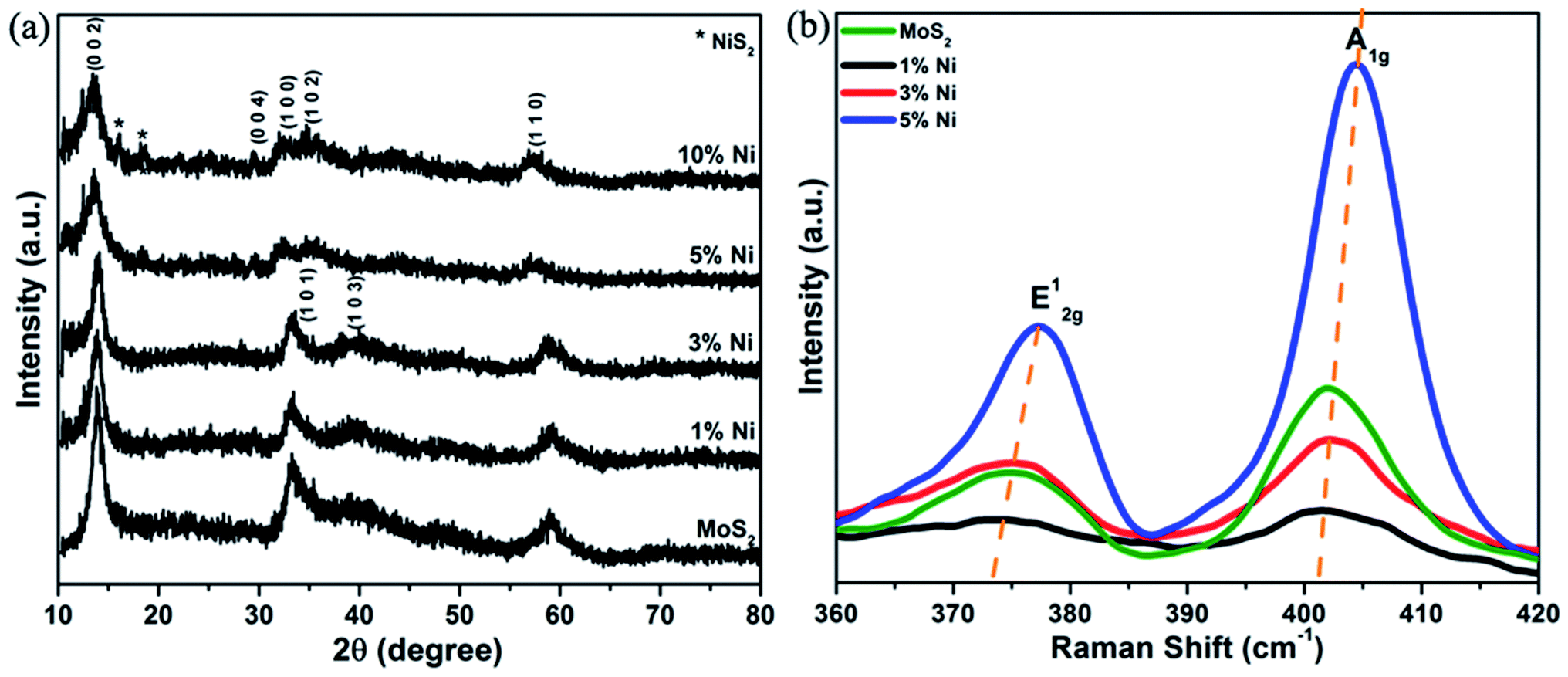 | ||
| Fig. 1 (a) XRD pattern and (b) Raman spectra of the Mo1−xNixS2 nanostructures. | ||
| Sample | Grain size (nm) | Lattice parameters (Å) | Interplanar spacing (d) (0 0 2) (Å) | |
|---|---|---|---|---|
| a | c | |||
| Bulk MoS2 [JCPDS no. 37-1492] | — | 3.16 | 12.29 | 6.16 |
| MoS2 | 6 | 3.13 | 12.69 | 6.35 |
| 1% Ni–MoS2 | 6 | 3.12 | 12.84 | 6.42 |
| 3% Ni–MoNiS2 | 6 | 3.13 | 12.76 | 6.38 |
| 5% Ni–MoNiS2 | 3 | 3.20 | 13.19 | 6.60 |
Micro-Raman studies were performed to investigate the number of layers and the effect of substitution of each facet. The difference in Raman shifts between the E12g and A1g Raman modes is sensitive to the number of layers and can be used to identify the number of layers in MoS2. The E12g mode corresponds to the in-plane vibration of two S atoms with respect to the Mo atom between them in the opposite direction, while the A1g mode is attributed to the out-of-plane vibration of only S atoms in opposite directions. The E12g mode is largely affected by the long-range interlayer coulombic interactions and structural variations, whereas the A1g mode is less affected by interlayer interactions. The A1g mode greatly corresponds to interlayer van der Waals forces.37 Our experimental results represented in Fig. 1(b) shows that both E12g and A1g modes of 1% Ni-substituted MoS2 undergo a red shift compared with pure MoS2. From Table 1, it was observed that for 1% Ni-substituted MoS2, the lattice parameter ‘a’ is slightly decreased and ‘c’ increased compared to pure and other Ni-substituted MoS2 nanostructures. This suggests that some slight disorientation and changes are taking place with the incorporation of Ni. Hence, the observed red-shifts in 1% Ni-substituted MoS2 can be attributed to the structural changes occurring upon substitution, whereas the Raman peaks of other samples show obvious shifts of both E12g and A1g modes with Ni substitution. The difference between these modes corresponds to the formation of few-layered MoS2, which was also further verified by photoluminescence measurements.38,39 With decreasing layer number, the interlayer van der Waals forces in MoS2 enhance the vibration of atoms, and as a result, both E12g and A1g modes showed a significant blue-shift. The enhancement in the A1g mode can be related to the strong electron-phonon coupling along the c-axis mainly due to the dz2 orbitals of Mo atoms. Also, the Raman spectra show an obvious increase in the intensity of the E12g and A1g modes associated with an increase in the thickness of the nanoflakes with Ni substitution, corresponding to surface reconstruction and vibrational softening. The Raman spectra thus demonstrated the successful synthesis of few-layered MoS2 nanoflakes with the incorporation of nickel.
The morphology of pure and Ni substituted MoS2 samples were studied from the FESEM images, as shown in Fig. 2. These show that the as-prepared pure and Ni-substituted MoS2 nanostructure exhibits 2D hierarchical curly sheet-like architecture with an average thickness of 10–15 nm. Energy dispersive X-ray (EDAX) measurement of the samples was performed to identify the chemical composition, as shown in Fig. 3. The observed presence of Ni, Mo and S supports the suggested formation of Mo1−xNixS2 nanosystems.
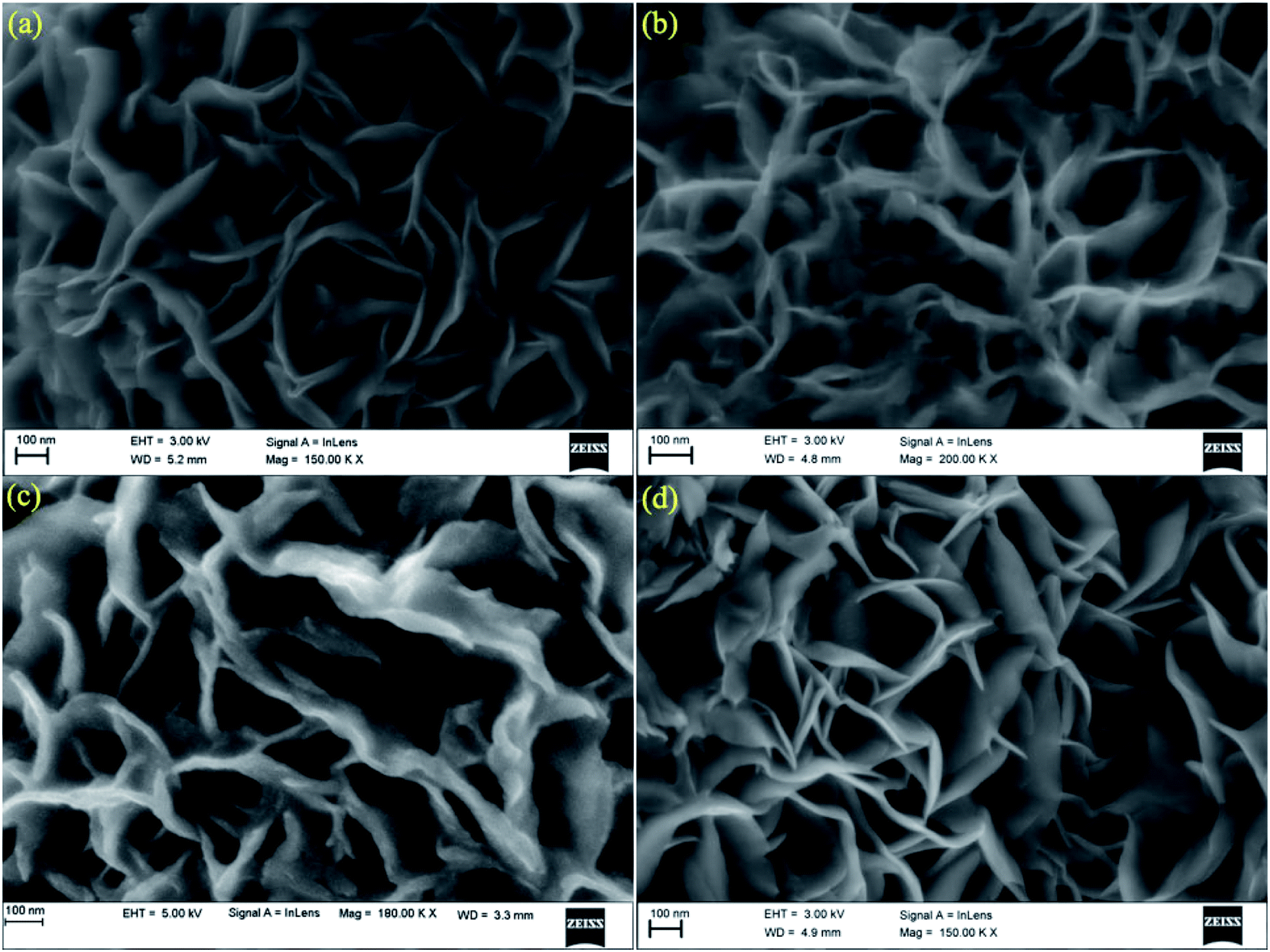 | ||
| Fig. 2 FE-SEM images of (a) pure (b) 1% Ni- (c) 3% Ni- and (d) 5% Ni-substituted MoS2 nanoflakes. | ||
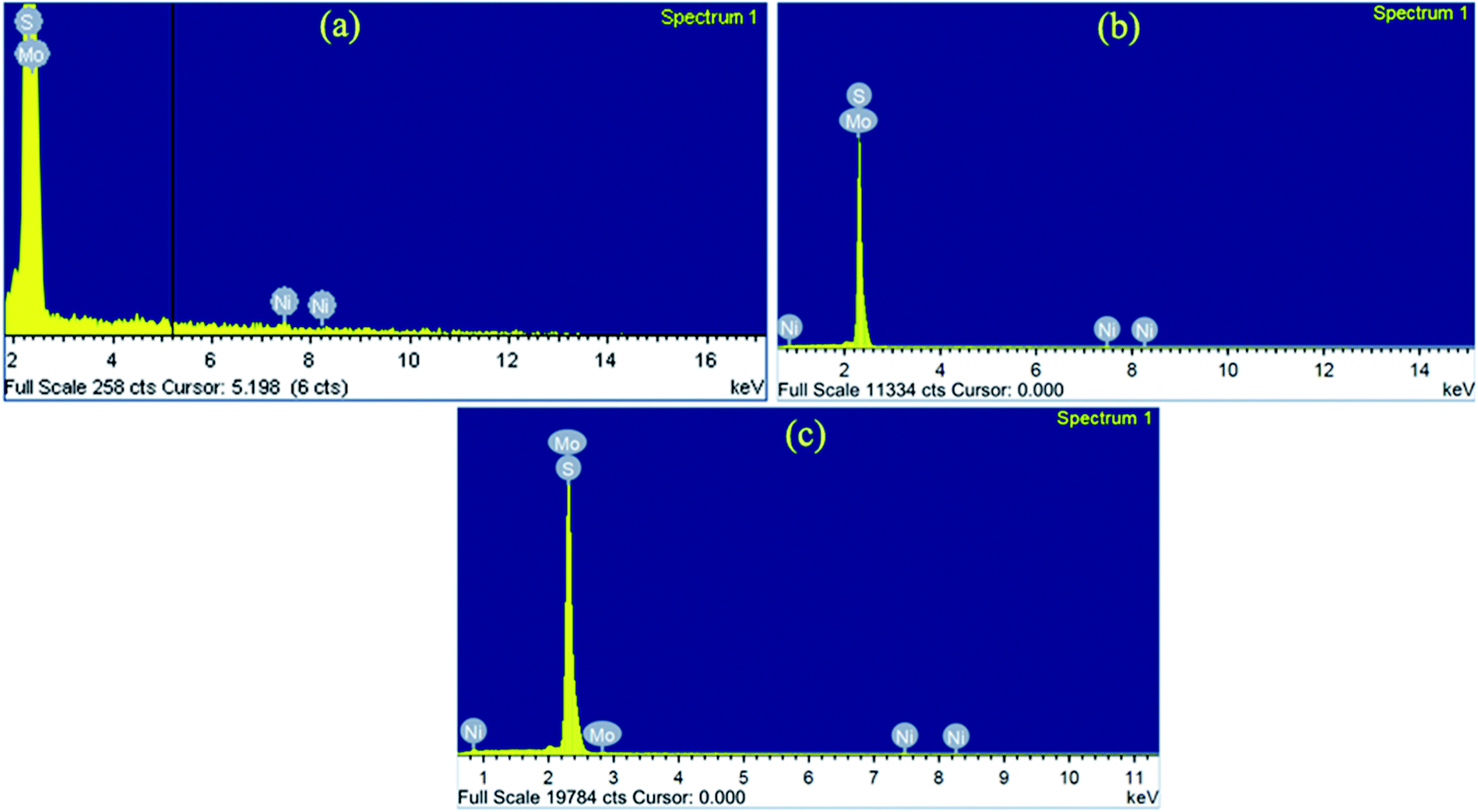 | ||
| Fig. 3 EDAX spectra of (a) 1% Ni- (b) 3% Ni- and (c) 5% Ni-substituted MoS2 nanoflakes. | ||
Fig. 4 displays the UV-vis-NIR absorption spectra of Mo1−xNixS2 nanostructures in aqueous dispersions. There are two optical absorption shoulder peaks in the visible region of MoS2 nanostructures: one around 600–700 nm, which is associated with the direct-gap optical excitation of A and B excitons between the maximum of the split valence bands and the minimum of the conduction band at the K point of the Brillouin zone; the other absorption peak at around 350–500 nm, which can be assigned to the direct transition from the deep valence band to the conduction band. The spin splitting is associated with the combined effect of interlayer interaction and strong spin–orbit coupling.
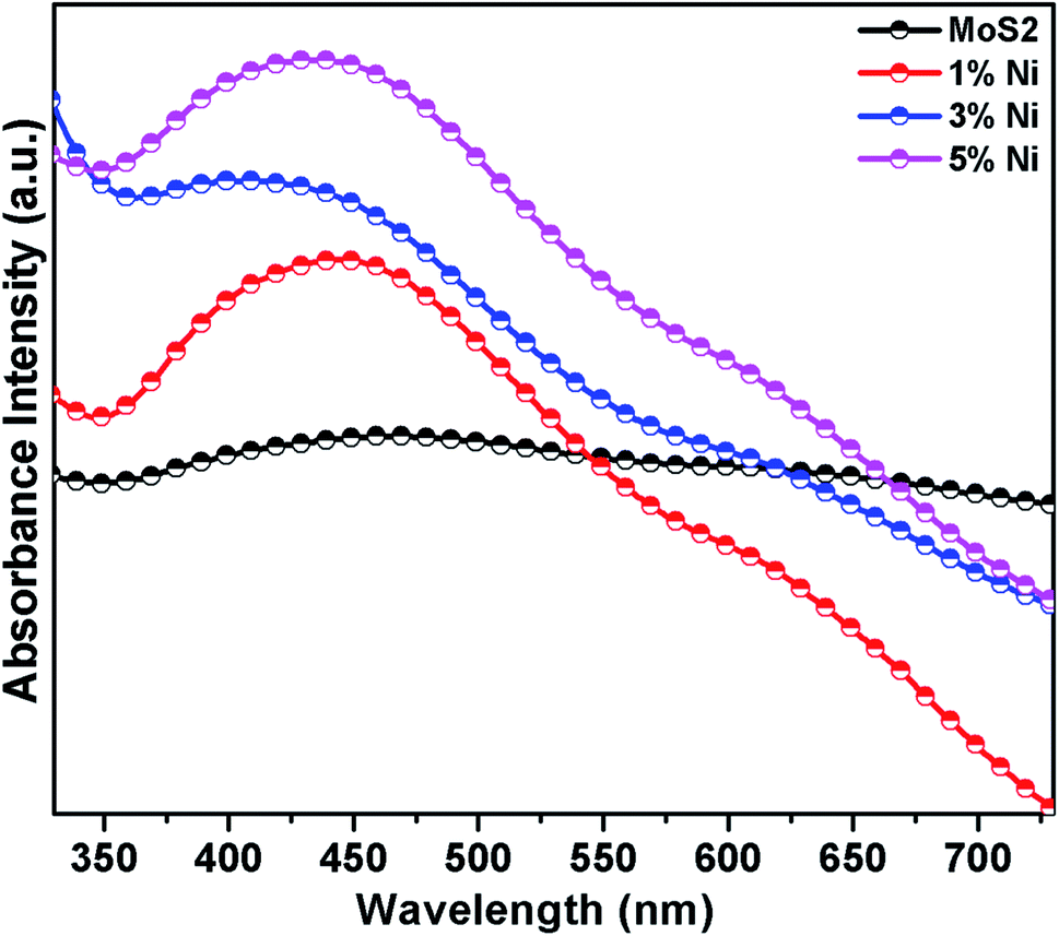 | ||
| Fig. 4 UV-vis-NIR absorption spectra of Mo1−xNixS2 nanoflakes. | ||
Large Coulomb interactions in low-dimensional 2D materials form stable excitons that play a significant role in the optical properties. Fig. 5(a) displays the down-conversion photoluminescence (PL) spectra of Mo1−xNixS2 nanoflakes excited at 450 nm. Prominent PL emissions were observed at 600 nm (2.07 eV) and 640 nm (1.94 eV) corresponding to the direct-gap transitions from the K-point of the Brillouin zone due to spin–orbit splitting in the valence band. An additional peak at 685 nm (1.81 eV) was also found to be associated with negative exciton (trion) due to some defects.40 The PL intensity was found to increase with increasing Ni concentration due to radiative recombination across the direct band gap,41 enabling improved possibilities in optical properties and optoelectronic device applications. The enhanced PL may be due to the charge transfer between Ni dopants and the 2D layers inducing shifts at the Fermi energy level.42
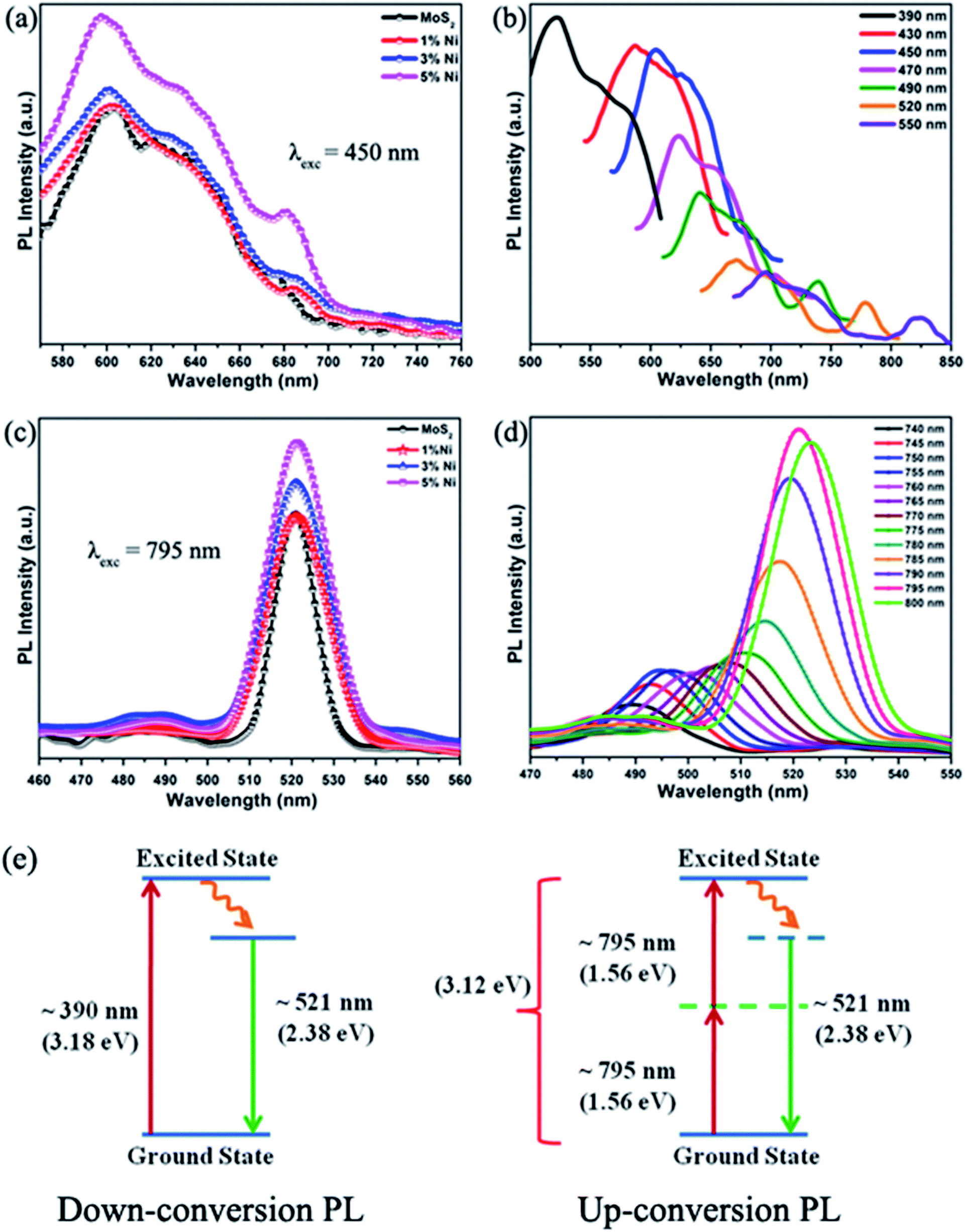 | ||
| Fig. 5 (a) Down-conversion (DC) PL spectra at an excitation of 450 nm for the Mo1−xNixS2 nanoflakes, (b) excitation wavelength-dependent DCPL of 1% Ni–MoS2, (c) up-conversion (UC) PL spectra at an excitation of 795 nm for the Mo1−xNixS2 nanoflakes, (d) excitation wavelength-dependent UCPL of 1% Ni–MoS2 and (e) schematic representation of the UC and DCPL mechanism. | ||
The most peculiar property observed in these MoS2 nanoflakes is that the fluorescence emission can be tuned by varying the excitation wavelength. When excited at various wavelengths ranging from 430 nm to 560 nm, the emission peaks of the MoS2 nanoflakes aqueous solution showed a large synchronous red-shift from 590 to 706 nm representing excitation wavelength-dependent PL (EWDPL) behavior, as shown in Fig. 5(b) for 1% Ni-substituted MoS2. Even though the exact reason for EWDPL is not clear, the polydispersity of 2D-Mo1−xNixS2 and the surface states are mainly assigned as the reasons for EWDPL.43,44 It is also assumed that the substitution of Ni can also produce additional surface states leading to traps or recombination sites. The formation of the S–Ni–S bond along with S–Mo–S may be a driving force for enhanced PL. Upon exciting the nanoparticles using a shorter wavelength, the electrons present in smaller particles become excited to the conduction band, whereas an increased excitation wavelength only excites electrons in larger particles with narrower band gaps, thus suggesting the polydispersity in MoS2 nanoflakes.45
Another important size-dependent electronic structure characteristic of 2D-MoS2 nanoflakes observed in this study is the up-conversion photoluminescence (UCPL) nature, i.e., the emission of photons having higher energies than the excitation energy. The UCPL of pure and Mo1−xNixS2 nanoflakes excited at a wavelength of 795 nm are shown in Fig. 5(c). Fig. 5(d) represents the UCPL spectra of 1% Ni-substituted MoS2 nanoflakes, in which the excitation wavelength encompasses a broad range from 740 nm to 800 nm with emission peaks ranging from 485 nm to 525 nm. With an excitation wavelength of 795 nm (1.56 eV), a strong emission is observed at 521 nm. The same emission wavelength is observed for a down-conversion excitation at 390 nm. Thus, we can state that the observed up-conversion is due to the transfer of energy by the sequential absorption of two photons, where the first photon is absorbed to excite the molecule to its resonant virtual state followed by the absorption of the second photon to reach the first excited state. This results in the direct transition from the ground state to the excited state causing a two-photon fluorescence emission at 521 nm. Our previous studies have explained in detail the UCPL in pure MoS2.46 This UCPL property, the ability to convert infrared light into visible light, of 2D-MoS2 can find applications in various fields, such as multicolor displays, biological chips, bioimaging systems,17,35 lasers, optical memory, solar cells, etc. Fig. 5(e) shows the schematic representation of the two-photon-induced up-conversion and the down-conversion PL of the MoS2 nanoflakes.
Fig. 6 shows the magnetization versus magnetic field (M–H) curve of pure and Mo1−xNixS2 nanostructures. Usually, bulk MoS2 samples are diamagnetic in nature. However, the as-prepared MoS2 nanostructures exhibit a ferromagnetic response in addition to a diamagnetic background, as shown in the inset of Fig. 6(a). The observance of magnetism can be attributed to the presence of unpaired spins in the host lattice of MoS2. In addition, the magnetic properties are highly dependent on the structure and size of the grains and crystallinity. The saturation magnetization was found to increase for 1%-Ni substituted MoS2, whereas with increasing nickel concentration, the magnetization was found to decrease, likely due to the antiferromagnetic nature of NiS2 structures. The observed ferromagnetic coupling in Mo1−xNixS2 can be explained in terms of the Zener's p–d hybridization mechanism for FM in dilute magnetic semiconductors.47 At low Ni substitution levels, the neighboring S atoms are spin-polarized, and the strong p–d hybridization between the Ni atom with its neighbouring S atoms results in a strong FM coupling between them. At high Ni concentrations, a decrease in the grain size is also noticed, which also represents a decrease in layer number in the case of MoS2, thus contributing to the variation in magnetization. A slight distortion in the hexagonal structure of MoS2 was also observed at higher concentrations, confirmed by the peak shift in XRD, contributing to the magnetic response in MoS2. Also, with increasing Ni concentration, the S–Ni–S interaction increases, which is antiferromagnetic (AFM) in nature.48 This AFM coupling between Ni and S atoms becomes stronger resulting in decreased magnetization at higher Ni substitutions. Hence, it is clear that the manifestation of surface effects plays a significant role in the magnetization of MoS2 nanoflakes.47
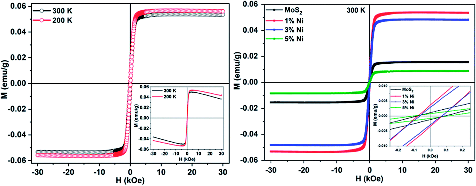 | ||
| Fig. 6 Magnetization vs. magnetic field (M–H curve) of (a) 1% Ni-substituted MoS2 nanoflakes measured at 200 and 300 K with the inset representing the magnetization curves before subtraction of the diamagnetic background and (b) Mo1−xNixS2 (x = 0, 1, 3, 5 wt%) nanoflakes measured at 300 K. | ||
The performance of the as-synthesized Mo1−xNixS2 samples was further thoroughly investigated in the electrocatalytic hydrogen evolution reaction (HER). Fig. 7(a) depicts the linear sweep voltammetry (LSV) curves of different Ni-substituted MoS2 samples recorded in N2 saturated 0.5 M H2SO4 at a scan rate of 2 mV s−1. To compare the HER activity, only MoS2 and commercially available benchmarked Pt/C catalyst (20 wt%/80 wt%) were also examined under identical conditions (Fig. 7(a)). It is observed that the performance of only MoS2 was relatively inferior to that of its Ni-substituted MoS2 counterparts, especially in regards to onset potential and current density (calculated using geometrical area). Furthermore, the percentage of Ni substituted into MoS2 had a substantial effect on the catalytic activities of the hybrid catalysts (Fig. 7(a)). Optimal catalytic activity is achieved in the 3% Ni–MoS2, as indicated by the low onset potential and high current density. The 3% Ni–MoS2 exhibited a low overpotential of 297 mV compared to that of MoS2 (418 mV), 1% Ni–MoS2 (392 mV) and 5% Ni–MoS2 (370 mV) at a current density of 1 mA cm−2 (based on the geometric area of the electrode). The comparison between only MoS2 and Mo1−xNixS2 reinforced the importance of Ni substitution for better catalytic performance. The near-zero hydrogen adsorption free energy of the Mo edge sites (ΔGH = 0.06 eV) makes them active sites for hydrogen evolution.49 Moreover, it has been also well confirmed that the doping of either transition metals (e.g., Ni or Co) into MoS2 or transition metals (e.g., Cu or Ni) used as a substrate for MoS2 could significantly enhance the HER performance of MoS2 in both acidic and alkaline mediums.34,50–53 Herein, the incorporation of Ni in the MoS2 catalyst was found to expose more active sites. Characteristically, in MoS2, the Mo edge was shown for its HER catalytic activity, while the S edges were found to be inert. However, it was shown by Yi Cui et al. that Ni doping has profound influence on the HER activity of MoS2.54 With the incorporation of Ni, the S edges also became active towards HER, and it was found that Ni substitution created two active sites (the most thermo-neutral site) unlike other transition metals such as Fe, Co, and Cu-doped MoS2. The experimentally observed enhanced HER activity of Ni-substituted MoS2 can be attributed to this gas-phase theoretical prediction, and a detailed theoretical study on the HER of the present system will be carried out in the near future after also consider the solvent effects.
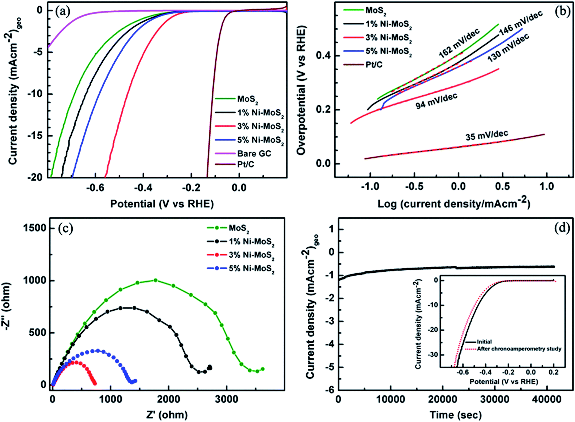 | ||
| Fig. 7 Electrochemical HER performance of the MoS2 and Ni-substituted MoS2 electrodes in 0.5 M H2SO4; (a) polarization curves; (b) Tafel plots obtained from the corresponding polarization curves (c) Nyquist plots; (d) chronoamperometric response of the 3% Ni–MoS2 electrode at the applied potential of −0.303 V (vs. RHE). Inset shows polarization curves of 3% Ni–MoS2 obtained before and after the chronoamperometric experiment. | ||
The increased HER activity of the Mo1−xNixS2 nanoflakes can probably be attributed to the enhancement of active sites due to the incorporation and replacement of Mo sites by Ni forming Mo1−xNixS2 and NiS2 phases. It was also expected that the Ni substitution in MoS2 would shift the ΔGH value closer to zero, thus establishing Mo1−xNixS2 nanostructures as an efficient HER catalyst.50,55 However, it is the number of active sites and the electron transfer capabilities that mainly determines the HER activity, henceforth, Tafel slopes were calculated from the corresponding polarization curves, as shown in Fig. 7(b). The slopes obtained from the linear part of the Tafel plots were 162, 146, 94, and 130 mV per decade for MoS2, 1% Ni–MoS2, 3% Ni–MoS2 and 5% Ni–MoS2, respectively. The relatively smaller Tafel slope obtained for 3% Ni–MoS2 compared to that of MoS2 and other Ni–MoS2 electrodes clearly suggests the low surface coverage of adsorbed hydrogen leading to faster reaction kinetics and excellent activity toward the HER at the 3% Ni–MoS2 electrode. The pure MoS2 catalyst was found to have a higher Tafel slope (162 mV per decade), representing a larger surface coverage (lower number of active sites or only the edges were active as was established for 2H–MoS2),56,57 and the reaction results in a recombination step. The exchange current density (j0) value can be further calculated by extrapolating the Tafel plot. The 3% Ni–MoS2 displays larger j0 value (8.5 × 10⁻³ mA cm−2), which is about 2.8 times larger than that of pristine MoS2 (2.2 × 10⁻³ mA cm−2). Thus, the earlier onset overpotential and smaller Tafel slope as well as the larger j0 clearly demonstrate that the catalytic activity of the 3% Ni–MoS2 electrode was better than that of the MoS2 and other Mo1−xNixS2 electrodes (Table S1†).
The Nyquist plots from the electrochemical impedance spectroscopy (EIS) were also applied to study the electrode kinetics under HER operating conditions (Fig. 7(c)), where all the catalysts were compared under the same applied potential. It was found that charger transfer resistance (Rct, semicircle part touching the real axis in the Nyquist plot) of 3% Ni–MoS2 (730 Ω) was less than that of MoS2 (3402 Ω), 1% MoS2 (2519 Ω) or 5% MoS2 (1400 Ω), which further support the idea that the improved HER activities at the 3% Ni–MoS2 electrode were due to the faster reaction kinetics of the HER. The electrochemical double-layer capacitances (Cdl) were also measured using cyclic voltammetry to evaluate the electrochemical surface area of the as-prepared Mo1−xNixS2 catalysts (Fig. S1, ESI†). The Cdl for 3% Ni–MoS2 is 8.2 mF cm−2, which is 2.2 times larger than that of pristine MoS2 (Table S1†) and larger than the other Mo1−xNixS2 counterparts. Such a high Cdl value for 3% Ni–MoS2 indicates the high electrochemical surface area and rich exposed catalytic active sites on the surface, which are further responsible for better HER performance.
Apart from low Rct and small Tafel slope, the Ni–MoS2 HER electrocatalyst should exhibit long-run stability under acidic conditions. To assess this, the durability of the 3% Ni–MoS2 catalyst was investigated by electrolysis at a constant potential of −0.303 V vs. RHE and by comparing the polarization curves measured before and after the electrolysis experiment. It was found that the current density remained almost unchanged even under continuous operation of more than 40![[thin space (1/6-em)]](https://www.rsc.org/images/entities/char_2009.gif) 000 seconds suggesting the excellent durability of the Mo1−xNixS2 for the HER. The polarization curves taken before and after the electrolysis experiments (inset of Fig. 7(d)) also show the negligible change in overpotential and current density, which further demonstrate the excellent catalytic durability of the catalyst electrode. The structural changes of Ni–MoS2 after the durability tests were also analysed by SEM and Raman measurements (Fig. S2 and S3†). It can be seen that there were no obvious changes in the surface morphology (Fig. S2†) and in the Raman in-plane (E12g) and out-of-plane (A1g) vibrations of MoS2 (Fig. S3†) even after >10 h of durability testing. These observations clearly demonstrate the excellent stability of the Mo1−xNixS2 electrode for the HER in acidic solutions. In addition, the HER performance of 3% Ni–MoS2 was also tested in alkaline (1 M KOH, pH = 13.7) as well as in neutral media (0.5 M Na2SO4, pH = 7.1), and the results are given in Fig. S4.† In alkaline media, the optimum 3% Ni–MoS2 electrode showed significant enhancement with an overpotential of 334 mV at 1 mA cm−2, which is nearly 190 mV lower than for pristine MoS2. However, in neutral media, the 3% Ni–MoS2 electrode did not shows any significant improvement in electrocatalytic HER activity compared to that of pristine MoS2. Further, knowing the fact that Pt wire as a counter electrode can promote the HER performance of the samples due to the shuttle and re-deposition of Pt seeds on the working electrode, we cross-checked the HER performance of 3% Ni–MoS2 obtained using a Pt wire counter electrode with a high surface area graphite rod counter electrode, and the results are shown in Fig. S5.† No significant changes were observed in the current densities/onset potentials while varying the counter electrode from the Pt wire to graphite, indicating its inherent catalytic activity toward HER.
000 seconds suggesting the excellent durability of the Mo1−xNixS2 for the HER. The polarization curves taken before and after the electrolysis experiments (inset of Fig. 7(d)) also show the negligible change in overpotential and current density, which further demonstrate the excellent catalytic durability of the catalyst electrode. The structural changes of Ni–MoS2 after the durability tests were also analysed by SEM and Raman measurements (Fig. S2 and S3†). It can be seen that there were no obvious changes in the surface morphology (Fig. S2†) and in the Raman in-plane (E12g) and out-of-plane (A1g) vibrations of MoS2 (Fig. S3†) even after >10 h of durability testing. These observations clearly demonstrate the excellent stability of the Mo1−xNixS2 electrode for the HER in acidic solutions. In addition, the HER performance of 3% Ni–MoS2 was also tested in alkaline (1 M KOH, pH = 13.7) as well as in neutral media (0.5 M Na2SO4, pH = 7.1), and the results are given in Fig. S4.† In alkaline media, the optimum 3% Ni–MoS2 electrode showed significant enhancement with an overpotential of 334 mV at 1 mA cm−2, which is nearly 190 mV lower than for pristine MoS2. However, in neutral media, the 3% Ni–MoS2 electrode did not shows any significant improvement in electrocatalytic HER activity compared to that of pristine MoS2. Further, knowing the fact that Pt wire as a counter electrode can promote the HER performance of the samples due to the shuttle and re-deposition of Pt seeds on the working electrode, we cross-checked the HER performance of 3% Ni–MoS2 obtained using a Pt wire counter electrode with a high surface area graphite rod counter electrode, and the results are shown in Fig. S5.† No significant changes were observed in the current densities/onset potentials while varying the counter electrode from the Pt wire to graphite, indicating its inherent catalytic activity toward HER.
Thus, all the above results suggest the as-synthesized 3% Ni substituted MoS2 as a promising HER catalyst. Ni-substituted Mo–S edges were found to enhance the structural stability and electronic structure of MoS2 nanostructures, thus tuning the conductivity of hybrid materials. The increased HER efficiency and substantial long-term stability of Mo1−xNixS2 suggests great promise in the fabrication of cost-effective and efficient H2 evolution electrodes in water electrolysis systems.
Conclusion
Engineering new functionalities in 2D materials can be easily achieved by the substitution of different materials enabling novel applications such as 2D magnonic devices. In this work, we successfully synthesized polycrystalline pure and Mo1−xNixS2 nanoflakes through a simple hydrothermal method without using any surfactants. A detailed investigation of the XRD data revealed that the grain size was found to be in the range of 3–6 nm, and the lattice parameters were found to increase with Ni substitution. The displacement of the XRD peaks clearly reflects the stacking and rotational disorder of the layers. Investigations of the E12g and A1g Raman shifts represent the existence of few layers of MoS2. Indirect-to-direct band gap transition at the K-point of the Brillouin zone was confirmed from the UV-vis-NIR absorption and photoluminescence emission spectra. Interestingly, an excitation wavelength-dependent direct and up-conversion PL was observed for the as-synthesized MoS2 and Mo1−xNixS2 nanoflakes. Magnetic measurements depicted the ferromagnetic nature of pure MoS2 arising from edge sites and variations due to the incorporation of nickel. The 3% Ni-substituted MoS2 catalyst also exhibited excellent HER activity superior to that of pure MoS2 and other Ni-substituted MoS2 samples.Conflicts of interest
There are no conflicts to declare.Acknowledgements
Levna Chacko acknowledges the Department of Science and Technology (DST), New Delhi, India for the INSPIRE Fellowship. T. N. N. and P. K. R. thank Tata Institute of Fundamental Research-Hyderabad, India for the financial support. P. K. R. also acknowledges the DST-SERB, India for the national postdoctoral fellowship (PDF/2016/001440). The authors acknowledge the Department of Science and Technology, Government of India under the Nanoscience and Technology Initiative for Raman facilities at CUSAT, Kerala.Notes and references
- M. J. Allen, V. C. Tung and R. B. Kaner, Chem. Rev., 2010, 110, 132–145 CrossRef CAS PubMed.
- K. S. Novoselov, V. I. Fal’ko, L. Colombo, P. R. Gellert, M. G. Schwab and K. Kim, Nature, 2012, 490, 192–200 CrossRef CAS PubMed.
- Q. H. Wang, K. Kalantar-Zadeh, A. Kis, J. N. Coleman and M. S. Strano, Nat. Nanotechnol., 2012, 7, 699–712 CrossRef CAS PubMed.
- S. Z. Butler, S. M. Hollen, L. Cao, Y. Cui, J. A. Gupta, H. R. Gutie, T. F. Heinz, S. S. Hong, J. Huang, A. F. Ismach, E. Johnston-halperin, M. Kuno, V. V Plashnitsa, R. D. Robinson, R. S. Ruoff, S. Salahuddin, J. Shan, L. Shi, O. M. G. Spencer, M. Terrones, W. Windl and J. E. Goldberger, ACS Nano, 2013, 7, 2898–2926 CrossRef CAS PubMed.
- J. K. Ellis, M. J. Lucero and G. E. Scuseria, Appl. Phys. Lett., 2011, 99, 261908 CrossRef.
- H. Terrones, E. Del Corro, S. Feng, J. M. Poumirol, D. Rhodes, D. Smirnov, N. R. Pradhan, Z. Lin, M. a T. Nguyen, a L. Elías, T. E. Mallouk, L. Balicas, M. a Pimenta and M. Terrones, Sci. Rep., 2014, 4, 4215 CrossRef CAS PubMed.
- R. Zhang, Y. Li, J. Qi and D. Gao, Nanoscale Res. Lett., 2014, 9, 586 CrossRef PubMed.
- D. Gao, M. Si, J. Li, J. Zhang, Z. Zhang, Z. Yang and D. Xue, Nanoscale Res. Lett., 2013, 8, 129 CrossRef PubMed.
- L. Cai, J. He, Q. Liu, T. Yao, L. Chen, W. Yan, F. Hu, Y. Jiang, Y. Zhao, T. Hu, Z. Sun and S. Wei, J. Am. Chem. Soc., 2015, 137, 2622–2627 CrossRef CAS PubMed.
- L. Chacko, A. K. Swetha, R. Anjana, M. K. Jayaraj and P. M. Aneesh, Mater. Res. Express, 2016, 3, 116102 CrossRef.
- J. Chang, S. Larentis, E. Tutuc, L. F. Register and S. K. Banerjee, Appl. Phys. Lett., 2014, 104, 141603 CrossRef.
- D. Ma, W. Ju, T. Li, X. Zhang, C. He, B. Ma, Y. Tang, Z. Lu and Z. Yang, Appl. Surf. Sci., 2015, 364, 181–189 CrossRef.
- Q. Yue, S. Chang, S. Qin and J. Li, Physics Letters, Section A: General, Atomic and Solid State Physics, 2013, 377, 1362–1367 CrossRef CAS.
- X. L. Fan, Y. R. An and W. J. Guo, Nanoscale Res. Lett., 2016, 11, 1–10 CrossRef PubMed.
- M. Luo, Y. H. Shen and J. H. Chu, Jpn. J. Appl. Phys., 2016, 55, 093001 CrossRef.
- B. Xia, Q. Guo, D. Gao, S. Shi and K. Tao, J. Phys. D: Appl. Phys., 2016, 49, 165003 CrossRef.
- H. Dong, S. Tang, Y. Hao, H. Yu, W. Dai, G. Zhao, Y. Cao, H. Lu, X. Zhang and H. Ju, ACS Appl. Mater. Interfaces, 2016, 8, 3107–3114 CrossRef CAS PubMed.
- J. Kibsgaard, Z. Chen, B. N. Reinecke and T. F. Jaramillo, Nat. Mater., 2012, 11, 963–969 CrossRef CAS PubMed.
- X. Wang, F. Nan, J. Zhao, T. Yang, T. Ge and K. Jiao, Biosens. Bioelectron., 2015, 64, 386–391 CrossRef CAS PubMed.
- X. Yu and K. Sivula, ACS Energy Lett., 2016, 1, 315–322 CrossRef CAS.
- O. Lopez-Sanchez, D. Lembke, M. Kayci, A. Radenovic and A. Kis, Nat. Nanotechnol., 2013, 8, 497–501 CrossRef CAS PubMed.
- J. Benson, M. Li, S. Wang, P. Wang and P. Papakonstantinou, ACS Appl. Mater. Interfaces, 2015, 7, 14113–14122 CrossRef CAS PubMed.
- D. He, Z. Kou, Y. Xiong, K. Cheng, X. Chen, M. Pan and S. Mu, Carbon, 2014, 66, 312–319 CrossRef CAS.
- Z. Kou, T. Meng, B. Guo, I. S. Amiinu, W. Li, J. Zhang and S. Mu, Adv. Funct. Mater., 2017, 27, 1604904 CrossRef.
- D. He, H. Tang, Z. Kou, M. Pan, X. Sun, J. Zhang and S. Mu, Adv. Funct. Mater., 2017, 29, 1601741 CrossRef PubMed.
- L. Irimpan, B. Krishnan, A. Deepthy, V. P. N. Nampoori and P. Radhakrishnan, J. Phys. D: Appl. Phys., 2007, 40, 5670–5674 CrossRef CAS.
- S. K. Cushing, M. Li, F. Huang and N. Wu, ACS Nano, 2014, 8, 1002–1013 CrossRef CAS PubMed.
- S. Zhu, J. Zhang, S. Tang, C. Qiao, L. Wang, H. Wang, X. Liu, B. Li, Y. Li, W. Yu, X. Wang, H. Sun and B. Yang, Adv. Funct. Mater., 2012, 22, 4732–4740 CrossRef CAS.
- H. Huang, C. Du, H. Shi, X. Feng, J. Li, Y. Tan and W. Song, Part. Part. Syst. Charact., 2015, 32, 72–79 CrossRef CAS.
- Z. Pu, S. Wei, Z. Chen and S. Mu, RSC Adv., 2016, 6, 11077–11080 RSC.
- I. S. Amiinu, Z. Pu, X. Liu, K. A. Owusu, H. G. R. Monestel, F. O. Boakye, H. Zhang and S. Mu, Adv. Funct. Mater., 2017, 27, 1702300 CrossRef.
- X. Xue, J. Zhang, I. A. Saana, J. Sun, Q. Xu and S. Mu, Nanoscale, 2018, 10, 16531–16538 RSC.
- J. Xie, H. Zhang, S. Li, R. Wang, X. Sun, M. Zhou, J. Zhou, X. W. (David) Lou and Y. Xie, Adv. Mater., 2013, 25, 1–7 CrossRef.
- D. Wang, X. Zhang, Y. Shen and Z. Wu, RSC Adv., 2016, 6, 16656–16661 RSC.
- S. Wang, Z. Wang, J. Qin, W. Wang, W. Li and D. He, Mater. Chem. Phys., 2011, 130, 170–174 CrossRef CAS.
- H. Akram, C. Mateos-Pedrero, E. Gallegos-Suárez, A. Guerrero-Ruíz, T. Chafik and I. Rodríguez-Ramos, Appl. Surf. Sci., 2014, 307, 319–326 CrossRef CAS.
- Y. Wang, C. Cong, C. Qiu and T. Yu, Small, 2013, 9, 2857–2861 CrossRef CAS PubMed.
- C. Lee, H. Yan, L. E. Brus, T. F. Heinz, J. Hone and S. Ryu, ACS Nano, 2010, 4, 2695–2700 CrossRef CAS PubMed.
- H. Li, Q. Zhang, C. C. R. Yap, B. K. Tay, T. H. T. Edwin, A. Olivier and D. Baillargeat, Adv. Funct. Mater., 2012, 22, 1385–1390 CrossRef CAS.
- S. S. Singha, D. Nandi and A. Singha, RSC Adv., 2015, 5, 24188–24193 RSC.
- R. Ganatra and Q. Zhang, ACS Nano, 2014, 8, 4074–4099 CrossRef CAS PubMed.
- S. Mouri, Y. Miyauchi and K. Matsuda, Nano Lett., 2013, 13, 5944–5948 CrossRef CAS PubMed.
- W. Gu, Y. Yan, X. Cao, C. Zhang, C. Ding and Y. Xian, J. Mater. Chem. B, 2016, 4, 27–31 RSC.
- W. Qiao, S. Yan, X. Song, X. Zhang, X. He, W. Zhong and Y. Du, Appl. Surf. Sci., 2015, 359, 130–136 CrossRef CAS.
- W. C. Zhang, X. L. Wu, H. T. Chen, J. Zhu and G. S. Huang, J. Appl. Phys., 2008, 103, 093718 CrossRef.
- L. Chacko, M. K. Jayaraj and P. M. Aneesh, J. Lumin., 2017, 192, 6–10 CrossRef CAS.
- M. Luo, S. Y. Hao and Y. T. Ling, AIP Adv., 2016, 6, 085112 CrossRef.
- R. Akbarzadeh, H. Dehghani and F. Behnoudnia, Dalton Trans., 2014, 43, 16745–16753 RSC.
- D. Escalera-López, Y. Niu, J. Yin, K. Cooke, N. V. Rees and R. E. Palmer, ACS Catal., 2016, 6, 6008–6017 CrossRef PubMed.
- J. Pan, C. Song, X. Wang, X. Yuan, Y. Fang, C. Guo, W. Zhao and F. Huang, Inorg. Chem. Front., 2017, 4, 1895–1899 RSC.
- J. Zhang, T. Wang, P. Liu, S. Liu, R. Dong, X. Zhuang, M. Chen and X. Feng, Energy Environ. Sci., 2016, 9, 2789–2793 RSC.
- P. K. Rastogi, S. Sarkar and D. Mandler, Appl. Mater. Today, 2017, 8, 44–53 CrossRef.
- C. Bae, T. A. Ho, H. Kim, S. Lee, S. Lim, M. Kim, H. Yoo, J. M. Montero-Moreno, J. H. Park and H. Shin, Sci. Adv., 2017, 3, e1602215 CrossRef PubMed.
- H. Wang, C. Tsai, D. Kong, K. Chan, F. Abild-Pedersen, J. K. Nørskov and Y. Cui, Nano Res., 2015, 8, 566–575 CrossRef CAS.
- S. Z. Qiao, Y. Zheng, Y. Jiao, M. Jaroniec and S. Z. Qiao, Angew. Chem., Int. Ed., 2014, 53, 2–16 CrossRef.
- D. Voiry, M. Salehi, R. Silva, T. Fujita, M. Chen, T. Asefa, V. B. Shenoy, G. Eda and M. Chhowalla, Nano Lett., 2013, 13, 6222–6227 CrossRef CAS PubMed.
- K. K. Tadi, A. M. Palve, S. Pal, P. M. Sudeep and T. N. Narayanan, Nanotechnology, 2016, 27, 275402 CrossRef PubMed.
Footnote |
| † Electronic supplementary information (ESI) available. See DOI: 10.1039/c9ra01869g |
| This journal is © The Royal Society of Chemistry 2019 |