
 Open Access Article
 This Open Access Article is licensed under a Creative Commons Attribution-Non Commercial 3.0 Unported Licence
Quantum-dot light-emitting diode with ultrathin Au electrode embedded in solution-processed phosphomolybdic acid†
Maciej Chrzanowski *,
Mateusz Banski,
Piotr Sitarek,
Jan Misiewicz and
Artur Podhorodecki*
*,
Mateusz Banski,
Piotr Sitarek,
Jan Misiewicz and
Artur Podhorodecki*
Department of Experimental Physics, Wroclaw University of Science and Technology, Wybrzeze Wyspianskiego 27, 50-370 Wroclaw, Poland. E-mail: maciej.chrzanowski@pwr.edu.pl; artur.p.podhorodecki@pwr.edu.pl
First published on 5th April 2019
Abstract
We proposed to exploit phosphomolybdic acid (PMA) as a cost-efficient MoOx source for combined spin-coating/sputtering/spin-coating deposition of a MoOx/Au/MoOx (MAM) composite electrode. The bottom PMA layer provides perfect wetting conditions for ultrathin Au film sputtering and prevents the formation of gold islands on the glass surface, while the top PMA layer helps to reduce light reflection. By optimizing the thickness of ultrathin Au films and PMA layers, we achieved maximum transmittance of 79% at 550 nm and a sheet resistance of only 22 Ω sq−1 which is comparable to the resistance of ITO substrates (20 Ω sq−1). MAM multilayer was explored both as a transparent electrode and as a hole injection layer (HIL) to eliminate ITO and PEDOT:PSS from solution-processed quantum-dot light-emitting diodes (QLEDs). The fabricated MAM-based QLED shows a peak external quantum efficiency (EQE) of 2.7% and maximum brightness of 12![[thin space (1/6-em)]](https://www.rsc.org/images/entities/char_2009.gif) 000 cd m−2 at 7 V. By performing bending tests of the polyethylene (PET) substrate coated with MAM electrode, we demonstrate that it is also a promising candidate for flexible transparent optoelectronics.
000 cd m−2 at 7 V. By performing bending tests of the polyethylene (PET) substrate coated with MAM electrode, we demonstrate that it is also a promising candidate for flexible transparent optoelectronics.
Introduction
Conductive transparent electrodes (CTE) are of great value for the fabrication of optoelectronic devices such as solar cells and displays.1,2 Besides high conductivity and transparency in the visible light region, the flexibility of CTE is highly desired. Currently, conductive oxides (indium tin oxide, ITO and fluorine doped tin oxide, FTO) are the most frequently used as a transparent electrode in optoelectronic devices. Although their transmission is negligible in the visible light region, its limitations including poor flexibility, high production costs, and low work function are still disruptive problems. Consequently, many alternative CTE have been explored including highly-conductive polymers, e.g. PEDOT:PSS,3,4 Ag nanowires,5 graphene,6–8 carbon nanotubes,9,10 metal grids,11,12 or hybrid structures.13,14Particular attention has been also devoted to ultrathin metal films which have been already demonstrated to work as efficient electrodes in both top- and bottom-emitting organic light-emitting diodes (OLEDs)15–18 and in top-emitting quantum-dot light-emitting diodes (QLEDs).19,20 Transmittance of ultrathin metal is considerably improved after embedding thin metal film in dielectric layers of vacuum-deposited high refractive index oxides which are responsible for reflectance reduction due to light coupling with surface plasmon polaritons (SPP) at a metal/oxide interface.21 These oxide/metal/oxide multilayers have been already investigated in various combinations including metal oxides: MoO3,22,23 WO3,24,25 ZnO,26 ZnS,27 as well as different metals: gold,28 silver,29 or copper.30 Although silver is the most promising metal due to its champion conductivity and low cost, it has a lower work function in contrast to gold which is tailored better to most of organic hole transport layers (HTLs).
In this paper, we propose to use cost-efficient solution-processed phosphomolybdic acid (PMA) instead of thermally evaporated MoO3 to fabricate MAM multilayer. We describe the procedure of deposition and transmittance optimization of ultrathin Au film embedded in PMA bilayer and demonstrate that it can be applied to regular bottom-emitting QLED where it serves as a bi-functional layer, i.e. transparent electrode and hole injection layer (HIL). In the end, the MAM electrode is examined in the context of flexible QLED fabrication.
Results and discussion
MAM multilayer optimization
Surface morphology of ultrathin metal films is particularly important for their electrical and optical properties, as it was already shown that discontinuous formations such as islands, grains, or perforations might have a detrimental effect on transparency and resistance.31–34 Deposition of nucleation layer has been recognized as an effective approach to improve the homogeneity of the metal film. Metal oxides or ultrathin metal layer is typically introduced to assure continuous layer growth, although other techniques, e.g. metal doping, have been also proposed.23 Molybdenum oxide (MoO3) is particularly favoured as a wetting layer because it can serve simultaneously as a hole injection layer (HIL) and is compatible with optoelectronic applications.We proposed to use combined sequential spin-coating/sputtering/spin-coating method to deposit MoOx/Au/MoOx multilayer electrode which is time-saving and cost-efficient compared to thermal evaporation. There are several solution-processed MoOx precursors including phosphomolybdic acid hydrate (PMAH),35 ammonium molybdate,36 molybdenyl acetylacetonate (MoO2(Acac)2),37 MoO3 nanoparticles,38 or peroxomolybdic acid.39 Among them, PMAH, which is heteropoly acid containing MoO3 units closed within Keggin structure, has been identified as particularly versatile MoOx precursor because of its high solubility in polar solvents, tunable work function, low thin film surface roughness, and relatively low post-annealing temperature.35,40 Importantly, PMA has been already examined as the HIL in organic photovoltaic cells (OPVs),41 OLEDs,35 and recently, also in QLEDs.42,43
During deposition of PMA/Au/PMA multilayer, we encountered a problem of dissolving the bottom PMA layer by the top PMA. To solve that problem, we used a procedure of PMA reduction by baking PMA before thin film deposition. The baking process under oxygen-free conditions causes partial reduction of Mo(VI) to Mo(V) which results in a gradual colour change from green to bluish (see Fig. S1a–c, ESI†). Reduced PMA has been already proposed as a post-annealing free HIL in OLED device,44 and it seems to be suitable for room-temperature processing of flexible conductive substrates. Reduced PMA is more soluble in acetonitrile (ACN) that in isopropanol (IPA), but we noticed that thin films prepared by spin-coating are easily flushed by ACN while IPA has no effect on film thickness. Additionally, the stability of reduced PMA is much better when stored in IPA.44
Except for Au, Ag thin film was also examined as a conductive interlayer but we discovered that PMA etches Ag due to its acidic nature forming a bluish solution which might indicate the reduction of Mo(VI) oxidation state to Mo(V). Although reduced PMA is no longer aggressive to Ag, its incorporation into PMA/Ag/PMA electrode requires further investigation and is beyond the scope of this paper.
Au films were deposited on cleaned quartz coated glass by sputtering with a constant rate and the thickness of films was determined by atomic force microscopy (AFM) (Fig. S2, ESI†). However, obtained Au films have poor transmittance especially in the longer wavelength region (Fig. 1a). The characteristic shape of transmission is readily attributed to the presence of Au grains instead of the continuous layer. The absorption in the blue wavelength region increases with thicker films and is affected by the absorption of light by interband electronic transitions.45 The maxima located at 500–520 nm are associated with light absorption on free electrons, whereas transmission minima in the red region of spectra might be explained by excitation of localized surface plasmon-polariton (SPP) which depends on size and shape of Au grains.46 The redshift of minima for thicker Au films is connected to a larger size of these grains. AFM image of Au film on glass reveals a corrugated surface with lots of perforations (Fig. S3a, ESI†). Such poor morphology might arise both from low wettability of glass and its rough surface (RMS = 1.0 nm). The sheet resistances of Au films deposited for 20 s and 19 s are 266 and 133 Ω sq−1, respectively, but they exceed 106 Ω sq−1 for all thinner samples indicating discontinuous nature of these films and lack of percolation pathways.
 | ||
| Fig. 1 (a) Transmittance of Au films with different thickness sputtered on quartz. (b) Sheet resistance of Au thin films with different thickness deposited on PMA or sandwiched between PMA films and annealed at 150 °C. | ||
In contrast to bare Au films, PMA/Au films have superior transmittance with a peak located between 550 and 600 nm (Fig. 1a). Minima in the red region, which are distinctive for SPP in grainy films, are no longer observed that suggests continuous films formation. The thicker Au film, the higher transmittance enhancement in the red region of the spectrum is observed. At the same time, absorption in the blue region increases. Sheet resistances of all PMA/Au bilayers are below 60 Ω sq−1 (Fig. 1b). Analysis of AFM images confirms that PMA, which surface has RMS roughness of only 0.22 nm, provides perfect conditions for continuous and smooth Au film growth (Fig. S3a, ESI†). RMS roughness of PMA/Au (shown in Fig. S3c, ESI†) is 0.33 nm and is much lower than Au on bare glass 0.48 nm. Both transmittance enhancement and sheet resistance reduction are the effect of continuous Au layer formation and support the claim that PMA enhances Au adhesion and supports grains coalescence. Results show that 1.2 nm of PMA layer is enough for transmittance enhancement in the visible light region and that thicker PMA layer has only a detrimental effect on transparency due to higher absorption of PMA in the UV range (Fig. S4a, ESI†).
Further optimization of the MAM electrode was performed by comparing sheet resistance and transmittance of as-deposited PMA/Au films. It was decided that around 7 nm Au (sputtered for 18 s) is a fair compromise between transmittance in the visible light region and sheet resistance which is comparable to that of ITO substrates (20 Ω sq−1). Selected sample was coated with top PMA layer resulting in a reduction of light reflection and further transmittance enhancement as shown in Fig. 2a. The effect of top PMA thickness on PMA/Au/PMA transmittance is shown in Fig. S4b (see ESI†). Optimum transmittance was achieved for PMA concentration of 15 mg ml−1 since the thicker film has started to reduce transmittance in the UV light region. It was discovered that top PMA helps to reduce sheet resistance after annealing at 150 °C. This effect might be attributed to the enhancement of conductivity as a result of welding of Au film discontinuities rather than PMA itself because no noticeable resistance reduction was observed for non-annealed PMA/Au. Complete MAM multilayer is yellowish due to high reflectance at the blue light range. The champion MAM electrode has a peak transmittance of 80% and a sheet resistance of 21.7 ± 0.5 Ω sq−1 (Fig. 2b).
 | ||
| Fig. 2 (a) Transmittance of selected Au and corresponding PMA/Au thin films before and after deposition of the top PMA layer. (b) Transmittance of different electrodes on glass substrates: ITO and optimized MAM multilayer with around 7 nm Au film. Vertical dotted line indicates the maximum of QLED EL spectrum. | ||
QLED device based on MAM electrode
Optimized PMA/Au/PMA multilayer was investigated as a transparent conductive electrode integrated with QLED. A reference device has following structure: ITO (100 nm), reduced PMA (10 nm), poly(N,N′-bis(4-butylphenyl)-N,N′-bis(phenyl)-benzidine) (p-TPD, 22 nm), poly(9-vinlycarbazole) (PVK, 8 nm), QDs (25 nm), sol–gel derived Zn0.85Mg0.15O (ZnMgO, 35 nm), and Al cathode (100 nm). QDs layer consists of 2 monolayers of green-emitting CdSe@ZnS/ZnS QDs with chemical composition-gradient structure and the average diameter of 13 nm which was determined from transmission electron microscopy (TEM) image (Fig. S5b, ESI†). The photoluminescence quantum yield (PL QY) of QDs is 55% and the PL peak is located at 515 nm (Fig. S5a, ESI†). Additionally, the second reference device was prepared using poly(3,4-ethylenedioxythiophene) polystyrene sulfonate (PEDOT:PSS, 40 nm) instead of PMA. The MAM-based device was fabricated on a glass substrate covered with PMA/Au/PMA multilayer. PMA/Au/PEDOT:PSS multilayer was not considered because of poor wettability of Au surface by PEDOT:PSS.Energy band diagram of QLED and scheme of the device are shown in Fig. 3a and b. The work function (WF) of reduced PMA after annealing is close to 5.8 eV, while the conduction band (CB) is located 0.5 eV above the Fermi level.44 The WF of typical Au film is in the range of 4.7–5.0 eV and does not differ significantly from ITO WF (4.7 eV). Small hole injection barrier is beneficial for charge generation at the HIL/HTL interface, where electrons are extracted from the HOMO level of p-TPD and transferred throughout CB of PMA towards Au electrode while generated holes are injected into the HTL. For all fabricated devices, sol–gel derived Zn1−xMgxO (x = 0.15) was applied as the electron transport layer (ETL). The optical bandgap of ZnMgO (3.5 eV) was estimated from absorbance (ABS) onset (see Fig. S6, ESI†), and the valence band maximum was assumed to be consistent with the previous report.47
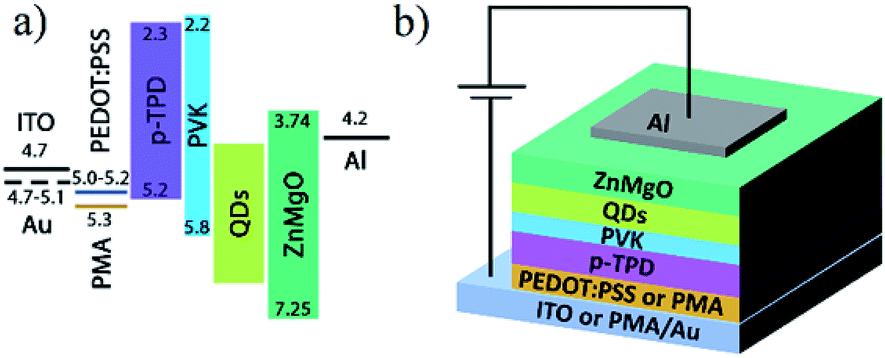 | ||
| Fig. 3 (a) Energy band diagram of regular QLED with two different anodes: ITO or Au. (b) Device architecture. | ||
The performance of the QLED devices with different electrodes is summarized in Fig. 4a and b. The turn-on voltages of all devices are nearly the same (2.5 V) and correspond closely to the bandgap of QDs (2.41 eV) which is calculated from ABS spectrum (Fig. S5a, ESI†). The maximum values of external quantum efficiency (EQE) at 100 mA cm−2 of a reference QLEDs fabricated on ITO substrates with reduced PMA and PEDOT:PSS are 5.9% and 4.0% respectively (Fig. 4b). Device with MAM electrode deposited on a glass substrate has EQE of 2.7%, although the luminance of all three devices is comparable. Electroluminescence (EL) spectrum of ITO-based QLED (shown in Fig. S8, ESI†) is not shifted relative to QDs PL spectrum but the tail in the longer wavelengths region of the spectrum is visible. For MAM-based QLED, this tail is smaller, probably due to a weak cavity effect. The angular emission patterns for both ITO and MAM-based devices were shown in Fig. S8 (ESI†). The Lambertian factor for standard ITO-based device was estimated at 0.94π and it is very close to standard Lambertian emission. The MAM-based device exhibits a factor of 0.76π that is related to more directional emission.
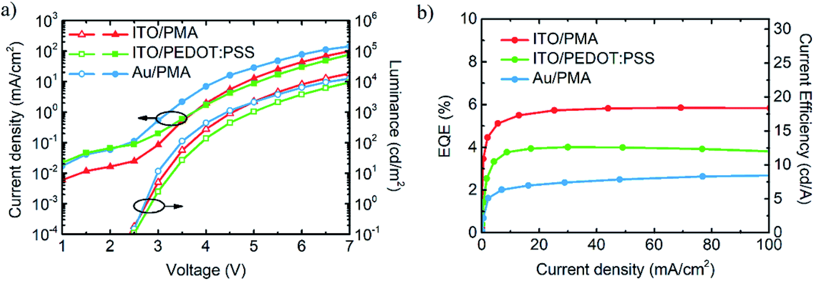 | ||
| Fig. 4 (a) Current density–voltage–luminance (J–V–L) characteristics of QLED device with ultrathin Au or ITO anode compared to standard device based on ITO/PEDOT:PSS. (b) EQE of the corresponding devices as a function of current density. | ||
Flexible QLED based on MAM electrode
We demonstrate that MAM multilayer electrode might be used for flexible QLED fabrication. Fig. 5a and b show MAM electrode on the glass and on the PET substrate. Bending tests were performed using different radii: 8 mm and 2 mm. For this aim, the custom-made bending machine was built (Fig. S8, ESI†). Sheet resistance measured after each number of cycles is shown in Fig. 6. In contrast to ITO-coated PET, sheet resistance of PET/MAM substrate is nearly insensitive to bending and it is increased by less than 10% after over 104 bending cycles using bending radius as small as 2 mm. | ||
| Fig. 5 Image of transparent MAM electrode on (a) glass and (b) flexible substrate. (c) Image of MAM-based flexible QLED at 7 V. | ||
 | ||
| Fig. 6 Relative sheet resistance of flexible substrate with ITO or MAM electrode as a function of number of bending cycles with different radius. | ||
Conclusions
To conclude, we have demonstrated a transparent conductive substrate composed of PMA/Au/PMA multilayer. The problem of the bottom PMA flushing was solved by PMA reduction. We discovered that the ultrathin PMA layer works as a wetting layer which enables uniform Au film to be sputtered. Based on these results, optimization of PMA/Au was performed, and we achieved a transmittance of 75% which was further enhanced after deposition of the top PMA. Consequently, complete PMA/Au/PMA multilayer exhibited a peak transmittance of 80% and a sheet resistance of 21.7 Ω sq−1. MAM was applied to QLED as a bi-functional layer to serve as the HIL and a transparent electrode. The EQE of 2.7% was achieved for MAM-based QLED, though its overall performance was lower than ITO-based counterpart which shows 5.7% EQE. However, an important advantage of MAM electrode was highlighted by demonstrating its superior durability during rigorous bending tests. We believe that the proposed fabrication method of MAM electrode using sequential spin-coating and sputtering could be extended to other large-scale printing methods which might be the next step towards the fabrication of transparent flexible devices.Experimental details
Materials
Reagents for the synthesis of QDs and sol–gel derived ZnMgO were delivered by Sigma-Aldrich and used as received, including cadmium oxide (CdO, 99.5%), selenium (99.99%), sulfur (99.98%), trioctylphosphine (TOP, 97%), zinc acetate (Zn(OAc)2, 99.99%), oleic acid (OA, 90%), oleylamine (OAm, 70%), 1-octadecene (ODE, 90%), magnesium acetate tetrahydrate (Mg(OAc)2·4H2O, 98.0%), monoethanolamine (MEA, 98.0%), and 2-methoxyethanol (99.8%). The materials for HTL deposition, p-TPD and PVK, were purchased from Ossila Ltd and Sigma Aldrich, respectively. PEDOT:PSS (AI 4083) was delivered by Ossila Ltd. Phosphomolybdic acid hydrate (H3[P(Mo3O10)4]·xH2O, PMAH, 99.9%) used for preparation of HTL was purchased from Sigma Aldrich.Preparation
Device fabrication
Devices were fabricated in the nitrogen-filled glovebox on either ITO or PMA/Au electrodes. ITO substrates were cleaned sequentially with detergent, deionized water, isopropanol, and were treated for 15 min in UV-ozone cleaner. PMA/Au substrates were used without any treatment. Reduced PMA was spin-coated (4000 rpm, 30 s) and annealed at 90 °C for 10 min. PEDOT:PSS was spin-coated (4000 rpm, 45 s) followed by baking at 150 °C for 10 min in air. Double HIL composed of p-TPD and PVK was deposited by sequential spin-coating of p-TPD (10 mg ml−1 in chlorobenzene) and PVK (2.5 mg ml−1 in 1,4-dioxane) at 4000 rpm for 30 s and each layer was annealed at 140 °C for 20 min. Then QDs dispersion (10 mg ml−1 in octane/hexane) was spin-coated at 2000 rpm for 20 s and annealed at 80 °C for 10 min. ZnMgO sol was spin-coated at 4000 rpm and formed a gel which was annealed at 150 °C for 15 min. Finally, 100 nm-thick Al cathodes were sputtered. An emitting area of a pixel was estimated at 4.5 mm2. For the flexible device, to prevent deformation of PET substrate, annealing temperatures of HTL and ETL were reduced to 110 °C.Measurements
J–V–L and EQE–J curves were measured using Keithley 2400 source-meter coupled with Konica Minolta LS-160 luminance meter. The angular emission pattern was measured using the luminance meter and a rotating stage. A calculated correction factor was used for EQE calculations. PL QY of QDs was estimated using the integration sphere (Gigahertz-Optic UPB-150-ART). UV-Vis PL spectra of QDs were collected by an optical fiber and recorded using CCD spectrometer (AvaSpec-ULS2048XL), and 405 nm laser diode was used for excitation. A deuterium–halogen lamp was a broadband light source for ABS measurements. The sheet resistance of conductive substrates was measured using Ossila Four-Point Probe System. High-resolution transmission microscopy (HR-TEM) image of QDs was taken by JEOL-ARM-200F microscope. The thickness of thin films was determined by Park Systems AFM.Conflicts of interest
There are no conflicts to declare.Acknowledgements
The authors acknowledge the National Science Centre for their financial support within the OPUS 14 project no. 2017/27/B/ST5/01209 and SONATA 8 project no. 2014/15/D/ST5/02744.Notes and references
- S. R. Forrest, Nature, 2004, 428, 911–918 CrossRef CAS PubMed.
- M. K. Choi, J. Yang, T. Hyeon and D.-H. Kim, npj Flexible Electronics, 2018, 2, 10 CrossRef.
- S.-H. Jeong, S.-H. Woo, T.-H. Han, M.-H. Park, H. Cho, Y.-H. Kim, H. Cho, H. Kim, S. Yoo and T.-W. Lee, NPG Asia Mater., 2017, 9, e411 CrossRef CAS.
- M. Vosgueritchian, D. J. Lipomi and Z. Bao, Adv. Funct. Mater., 2012, 22, 421–428 CrossRef CAS.
- J. Krantz, T. Stubhan, M. Richter, S. Spallek, I. Litzov, G. J. Matt, E. Spiecker and C. J. Brabec, Adv. Funct. Mater., 2013, 23, 1711–1717 CrossRef CAS.
- T.-H. Han, Y. Lee, M.-R. Choi, S.-H. Woo, S.-H. Bae, B. H. Hong, J.-H. Ahn and T.-W. Lee, Nat. Photonics, 2012, 6, 105–110 CrossRef CAS.
- S. Bae, H. Kim, Y. Lee, X. Xu, J.-S. Park, Y. Zheng, J. Balakrishnan, T. Lei, H. Ri Kim, Y. Il Song, Y.-J. Kim, K. S. Kim, B. Özyilmaz, J.-H. Ahn, B. H. Hong and S. Iijima, Nat. Nanotechnol., 2010, 5, 574–578 CrossRef CAS PubMed.
- K. S. Kim, Y. Zhao, H. Jang, S. Y. Lee, J. M. Kim, K. S. Kim, J.-H. Ahn, P. Kim, J.-Y. Choi and B. H. Hong, Nature, 2009, 457, 706–710 CrossRef CAS PubMed.
- O. Urper, İ. Çakmak and N. Karatepe, Mater. Lett., 2018, 223, 210–214 CrossRef CAS.
- Z. Wu, Z. Chen, X. Du, J. M. Logan, J. Sippel, M. Nikolou, K. Kamaras, J. R. Reynolds, D. B. Tanner, A. F. Hebard and A. G. Rinzler, Science, 2004, 305, 1273–1276 CrossRef CAS PubMed.
- M.-G. Kang, M.-S. Kim, J. Kim and L. J. Guo, Adv. Mater., 2008, 20, 4408–4413 CrossRef CAS.
- J.-S. Yu, G. H. Jung, J. Jo, J. S. Kim, J. W. Kim, S.-W. Kwak, J.-L. Lee, I. Kim and D. Kim, Sol. Energy Mater. Sol. Cells, 2013, 109, 142–147 CrossRef CAS.
- R. Wang, C. Fan, Z. Xiong, X. Yang and G. E. Jabbour, Org. Electron., 2015, 19, 105–112 CrossRef CAS.
- J. Jin, J. Lee, S. Jeong, S. Yang, J.-H. Ko, H.-G. Im, S.-W. Baek, J.-Y. Lee and B.-S. Bae, Energy Environ. Sci., 2013, 6, 1811 RSC.
- W. Cao, Y. Zheng, Z. Li, E. Wrzesniewski, W. T. Hammond and J. Xue, Org. Electron., 2012, 13, 2221–2228 CrossRef CAS.
- B. Tian, G. Williams, D. Ban and H. Aziz, J. Appl. Phys., 2011, 110, 104507 CrossRef.
- S. Lenk, T. Schwab, S. Schubert, L. Müller-Meskamp, K. Leo, M. C. Gather and S. Reineke, Appl. Phys. Lett., 2015, 107, 163302 CrossRef.
- D. Jeong, C. Lim, M. Kim, K. Jeong, J.-H. Kim, J. Kim, J.-G. Park, K.-S. Min and J. Lee, Electron. Mater. Lett., 2017, 13, 16–24 CrossRef.
- X. Yang, E. Mutlugun, C. Dang, K. Dev, Y. Gao, S. T. Tan, X. W. Sun and H. V. Demir, ACS Nano, 2014, 8, 8224–8231 CrossRef CAS PubMed.
- G. Liu, X. Zhou and S. Chen, ACS Appl. Mater. Interfaces, 2016, 8, 16768–16775 CrossRef CAS PubMed.
- T. W. Ebbesen, H. J. Lezec, H. F. Ghaemi, T. Thio and P. A. Wolff, Nature, 1998, 391, 667–669 CrossRef CAS.
- M. Maniruzzaman, M. A. Rahman, K. Jeong, H. Nam and J. Lee, Renewable Energy, 2014, 71, 193–199 CrossRef CAS.
- L. Shi, Y. Cui, Y. Gao, W. Wang, Y. Zhang, F. Zhu, Y. Hao, L. Shi, Y. Cui, Y. Gao, W. Wang, Y. Zhang, F. Zhu and Y. Hao, Nanomaterials, 2018, 8, 473 CrossRef PubMed.
- R. Capelli, S. Toffanin, G. Generali, H. Usta, A. Facchetti and M. Muccini, Nat. Mater., 2010, 9, 496–503 CrossRef CAS PubMed.
- T.-H. Yeh, C.-C. Lee, C.-J. Shih, G. Kumar, S. Biring and S.-W. Liu, Org. Electron., 2018, 59, 266–271 CrossRef CAS.
- H. W. Choi, N. D. Theodore and T. L. Alford, Sol. Energy Mater. Sol. Cells, 2013, 117, 446–450 CrossRef CAS.
- X. Liu, X. Cai, J. Qiao 1, J. Mao and N. Jiang 1, Thin Solid Films, 2003, 441, 200–206 CrossRef CAS.
- M. Maniruzzaman, M. Arifur Rahman, K. Jeong and J. Lee, Mater. Sci. Semicond. Process., 2014, 27, 114–120 CrossRef CAS.
- X. Yang, P. Gao, Z. Yang, J. Zhu, F. Huang and J. Ye, Sci. Rep., 2017, 7, 44576 CrossRef CAS PubMed.
- D. Ebner, M. Bauch and T. Dimopoulos, Opt. Express, 2017, 25, A240 CrossRef CAS PubMed.
- R. Henriquez, S. Bravo, R. Roco, V. Del Campo, D. Kroeger and P. Häberle, Metall. Mater. Trans. A, 2019, 50, 493–503 CrossRef.
- S. Hafezian, B. Baloukas and L. Martinu, Appl. Opt., 2014, 53, 5367 CrossRef PubMed.
- P. Malinský, P. Slepička, V. Hnatowicz and V. Svorčík, Nanoscale Res. Lett., 2012, 7, 241 CrossRef PubMed.
- J. Siegel, O. Lyutakov, V. Rybka, Z. Kolská and V. Švorčík, Nanoscale Res. Lett., 2011, 6, 96 CrossRef PubMed.
- S. Ohisa, S. Kagami, Y.-J. Pu, T. Chiba and J. Kido, ACS Appl. Mater. Interfaces, 2016, 8, 20946–20954 CrossRef CAS PubMed.
- W. Qiu, A. Hadipour, R. Müller, B. Conings, H.-G. Boyen, P. Heremans and L. Froyen, ACS Appl. Mater. Interfaces, 2014, 6, 16335–16343 CrossRef CAS PubMed.
- K. Zilberberg, H. Gharbi, A. Behrendt, S. Trost and T. Riedl, ACS Appl. Mater. Interfaces, 2012, 4, 1164–1168 CrossRef CAS PubMed.
- J. Meyer, R. Khalandovsky, P. Görrn and A. Kahn, Adv. Mater., 2011, 23, 70–73 CrossRef CAS PubMed.
- Y. Li, H. Yu, X. Huang, Z. Wu and M. Chen, RSC Adv., 2017, 7, 7890–7900 RSC.
- Y. Zhu, Z. Yuan, W. Cui, Z. Wu, Q. Sun, S. Wang, Z. Kang and B. Sun, J. Mater. Chem. A, 2014, 2, 1436–1442 RSC.
- X. Jia, L. Shen, M. Yao, Y. Liu, W. Yu, W. Guo and S. Ruan, ACS Appl. Mater. Interfaces, 2015, 7, 5367–5372 CrossRef CAS PubMed.
- Y. Liu, C. Jiang, C. Song, J. Wang, L. Mu, Z. He, Z. Zhong, Y. Cun, C. Mai, J. Wang, J. Peng and Y. Cao, ACS Nano, 2018, 12, 1564–1570 CrossRef CAS PubMed.
- D. Dong, L. Lian, H. Wang and G. He, Org. Electron., 2018, 62, 320–326 CrossRef CAS.
- S. Ohisa, K. Endo, K. Kasuga, M. Suzuki, T. Chiba, Y.-J. Pu and J. Kido, Inorg. Chem., 2018, 57, 1950–1957 CrossRef CAS PubMed.
- K. Sivaramakrishnan and T. L. Alford, Appl. Phys. Lett., 2010, 96, 201109 CrossRef.
- A. Axelevitch, B. Apter and G. Golan, Opt. Express, 2013, 21, 4126 CrossRef CAS PubMed.
- L. Hu, D.-B. Li, L. Gao, H. Tan, C. Chen, K. Li, M. Li, J.-B. Han, H. Song, H. Liu and J. Tang, Adv. Funct. Mater., 2016, 26, 1899–1907 CrossRef CAS.
- K.-H. Lee, J.-H. Lee, H.-D. Kang, B. Park, Y. Kwon, H. Ko, C. Lee, J. Lee and H. Yang, ACS Nano, 2014, 8, 4893–4901 CrossRef CAS PubMed.
Footnote |
| † Electronic supplementary information (ESI) available. See DOI: 10.1039/c9ra01680e |
| This journal is © The Royal Society of Chemistry 2019 |