 Open Access Article
Centimeter-scale 2D perovskite (PEA)2PbBr4 single crystal plates grown by a seeded solution method for photodetectors†
Chaoyang Ge ,
Wenhao Zhai
 ,
Cheng Tian,
Shiqi Zhao,
Tong Guo,
Shuren Sun,
Weixi Chen and
Guangzhao Ran*
State Key Laboratory for Artificial Microstructure and Mesoscopic Physics, School of Physics, Peking University, Beijing 100871, China. E-mail: rangz@pku.edu.cn
First published on 29th May 2019
Abstract
Large-sized single-crystal two-dimensional (2D) perovskites are highly desirable owing to their fundamental properties and intriguing ability to boost devices. Herein, 2-phenylethylammonium lead bromide [(PEA)2PbBr4] single crystals, which are a violet-light-emitting 2D perovskite material, with typical lateral sizes of about one centimeter were successfully grown using a seeded solution method. The single-crystal plates showed a well-defined shape (rectangle or hexagon), a natural thickness (300–500 μm) similar to that of conventional silicon and InP wafers, a large aspect ratio of ∼20, and a smooth surface (root mean square, ∼0.7 nm). We integrated these single crystal plates into an ultraviolet photodetector, achieving a low dark current of ∼10−13 A and an efficient photoresponse (on/off ratio, ∼103). This experiment could easily be extended to grow freestanding 2D perovskite single crystals on a wafer scale for practical integrated optoelectronics.
Introduction
Organic–inorganic hybrid lead halide perovskites are becoming a hot topic in materials science owing to their solution-based synthesis processes and promising applications in light harvesting and light generation.1–4In the perovskite family, 2D perovskites naturally form a quantum-well structure with inorganic semiconductor sheets of PbX4 (X = Cl, Br, or I) as wells and organic layers as dielectric barriers, which further tailor their electronic structure properties.5–7 For example, compared with 3D perovskites, 2D perovskites have a higher exciton binding energy and much lower self-doping level, making them excellent candidates for nanoscale lasers and high-performance photodetectors with ultralow thresholds and dark currents, respectively. Furthermore, 2D perovskites exhibit improved thermal stability and moisture resistivity.8,9
In previous studies, most 2D perovskites were polycrystalline films,10–13 which suffer from high trap and grain boundary densities. In contrast, single crystals possess much better optoelectrical properties than their polycrystalline counterparts,14 which has triggered increasing interest in the growth of 2D perovskite single crystals.
Many techniques have been used to grow large-sized 3D hybrid halide perovskite bulk single crystals.15–18 For example, Dang et al. and Lian et al. adopted a bottom seeded solution temperature-lowering (STL) growth method to grow MAPbI3 single crystals with centimeter sizes.19,20 By combining an inverse temperature crystallization method and repeated seeded growth method, Liu et al. grew extra-large MAPbI3 single crystals21 of up to 120 mm22 and FAPbI3 single crystals of 20 mm.23 MAPbBr3 single crystals with a sizes of 44 mm × 49 mm × 17 mm have also been harvested using a low-temperature-gradient crystallization approach.24 Furthermore, smart strategies have been reported to fabricate large-sized single-crystal thin films.25–27
However, directly extending these methods28–31 to 2D growth is difficult.32–40 The existing growth methods for (PEA)2PbBr4 single crystals mainly involve converting polycrystalline thin film to single-crystal nanoplates. Liang et al. and Zhai et al. adopted a solvent vapor-assisted method to convert spin-coated 2D perovskite (PEA)2PbBr4 thin films into well-defined single-crystal microplates,34,37 but these methods tended to grow single crystals with small sizes (∼10 μm). Wang et al. reported a fast synthetic method for preparing inch-scale 2D perovskite single-crystal membranes, which takes advantage of the spontaneous alignment of alkylammonium precursor cations and the high chemical potentials of the precursors molecules at the water–air interface.39 However, the resulting samples had irregular shapes and were too thin to be used without a support substrate. More recently, Zhang et al. reported a 200 mm2 (PEA)2PbBr4 single crystal prepared using a controlled evaporation process.40
Herein, large-sized single crystals of (PEA)2PbBr4 were grown using a combing STL and seed crystal method. The single crystal had a large aspect ratio (∼20) caused by anisotropic growth. The absorption spectrum was unique owing to the absorption of the organic layer. The photoluminescence (PL) lifetime was longer than those of the thin films, nanoplates, and single crystals reported previously. Finally, we successfully integrated this single crystal plate into a photodetector.
Experimental
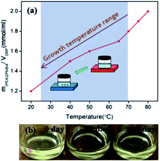
The growth method was based on the positive slope of the solubility curve of (PEA)2PbBr4 in N,N-dimethylformamide (DMF), as shown in Fig. 1(a).Remarkably, the solubility decreased almost two-fold upon cooling from 80 to 20 °C. The growth process consisted of two steps, as follows: (i) obtaining small single crystal seeds by naturally cooling the saturated solution, and (ii) seed crystals freely growing into large single crystals at room temperature. The precursor solution (1.8 M) was prepared by mixing PEABr and PbBr2 in a 2![[thin space (1/6-em)]](https://www.rsc.org/images/entities/char_2009.gif) :
:![[thin space (1/6-em)]](https://www.rsc.org/images/entities/char_2009.gif) 1 molar ratio in DMF in a vial and then heating with a hot plate to 70 °C under constant stirring. Once the precursors had dissolved completely, the hot plate was switched off. As the solution temperature dropped from 70 to 25 °C to induce solute saturation, small (∼1 mm) single crystal microplates were precipitated within a day. A suitable microplate was then selected as the seed crystal and placed into freshly saturated precursor solution in another vial. The seed crystal grew to a centimeter in size in three days. The growth process is illustrated by three snapshots at different intervals in Fig. 1(b).
1 molar ratio in DMF in a vial and then heating with a hot plate to 70 °C under constant stirring. Once the precursors had dissolved completely, the hot plate was switched off. As the solution temperature dropped from 70 to 25 °C to induce solute saturation, small (∼1 mm) single crystal microplates were precipitated within a day. A suitable microplate was then selected as the seed crystal and placed into freshly saturated precursor solution in another vial. The seed crystal grew to a centimeter in size in three days. The growth process is illustrated by three snapshots at different intervals in Fig. 1(b).
Compared with the previously reported STL method,19 no acid was involved in these experiments, making it easier to operate and improving the material utilization rate. The average productivity (ratio of final crystal mass to that of the initial precursor) was about 34.33% in four experiments, which was higher than the theoretical expectation (∼33.33%), which was attributed to solvent evaporation during the crystal growth process. Furthermore, the precursor solution was recyclable, allowing solvent and precursor overconsumption to be minimized.
Results and discussion
Fig. 2(a) shows a photograph of two (PEA)2PbBr4 single crystal plates grown for one week. The left plate had a well-aligned quasi-rectangular shape with a side length of about 8 mm, while the right plate had a hexagon shape with a maximum diagonal length greater than 1.0 cm. Their thicknesses were about 380 μm (as shown in Fig. 2(b)), which corresponded to an aspect ratio of ∼20. The aspect ratio has a significant impact on device fabrication and performance.41 Bulk 3D perovskite single crystals currently available do not usually allow for direct device fabrication. To solve this problem, Chen et al. developed a space-confined method to obtain single-crystal thin films with large aspect ratios,26 and Liu et al. used a diamond-wire sawing process to slice bulky crystals into thin wafers.23 In contrast, depending on anisotropic growth in solution, the (PEA)2PbBr4 single crystals obtained in this study were freestanding and ready for device fabrication. The single-crystal surface had a root mean square roughness of 0.702 nm within a 5 × 5 μm2 area characterized by atomic force microscopy (AFM), as shown in Fig. 2(c).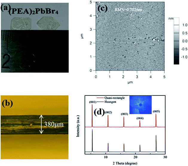 | ||
| Fig. 2 (a) An optical image of a (PEA)2PbBr4 single crystal; (b) single crystal lateral side; (c) AFM image; and (d) XRD 2θ scan patterns. Inset: (00l) direction. | ||
X-ray diffractometry (XRD) is a powerful tool for examining single-crystal quality. X-ray 2θ scan patterns of the single-crystal plates with two shapes on the top surface are shown in Fig. 2(d). The same XRD patterns concluded that these plates had identical crystal structures. The highest diffraction peaks at 5.36°, 10.66°, 15.98°, 21.34°, and 26.76° were assigned to the (001), (002), (003), (004), and (005) lattice planes of the layered (PEA)2PbBr4 structure, respectively.37 The dominance of the (00l) peaks in the XRD patterns suggested that the c-axis was the normal direction of the plate. The inset of Fig. 2(d) was the diffraction pattern in the (00l) direction.
We also studied the absorption and PL of (PEA)2PbBr4 single crystals. Absorption spectra of the single crystal and polycrystalline thin film are shown as solid green and dotted blue lines in Fig. 3(a), respectively. The absorption spectrum of the thin film indicated a single strong excitonic peak at 402 nm, as reported previously,42 which was considerably larger than its band edge.43 In contrast, the absorption spectrum of the single crystal showed two main peaks at 422.5 nm (peak 1) and 395.5 nm (peak 2), which was similar to the results for (C6H5CH2NH3)2PbI4 (ref. 6) and (PEA)2PbBr4 nanoplates.34 Peak 1 appeared at a lower energy than the PL peak of the single crystal, indicating that it might be caused by organic layer absorption, which had no corresponding downward radiative transitions. Meanwhile, peak 2, at a shorter wavelength, was attributed to intrinsic exciton absorption.34
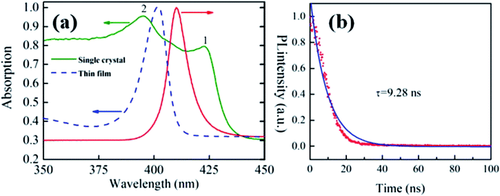 | ||
| Fig. 3 (a) Absorption spectra of a single crystal (green) and polycrystalline thin film (blue), and PL data from a single crystal (red); (b) time-resolved PL decay. | ||
The PL lifetime was measured to be 9.28 ns using a time-resolved spectrometer with pulsed 325 nm laser excitation, as shown in Fig. 3(b), which was much longer than those reported for polycrystalline thin films (0.62 ± 0.1 ns),34 nanoplates (1.27 ± 0.02 ns),34 and single crystals prepared using the poor-solvent diffusion method (5.1 ns).42 This indicated a longer carrier diffusion length and a lower nonradiative combination rate in the larger single crystals.44
Temperature-dependent PL spectroscopy can provide information about phase transitions and optically active defects. The temperature-dependent PL spectra of the (PEA)2PbBr4 single crystal from liquid nitrogen temperature (78 K) to room temperature (298 K) are shown in Fig. 4(a). The PL spectrum at each temperature had only a single peak, and the broad defect-related emission reported for (PEA)2PbBr4 microplate in ref. 37 was not observed here. Furthermore, the peak intensities increased from 78 to 178 K, reaching a maximum, known as negative thermal quenching behavior,45 and then decreasing (Fig. 4(b)), while the band gap peak was slightly red shifted as the temperature increased, as observed for most semiconductors (Fig. 4(c)). Additionally, after being exposed to ambient air for four weeks, the single crystal sample showed no obvious degradation, and its PL intensity remained stable.
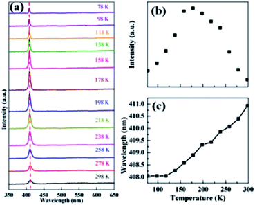 | ||
| Fig. 4 (a) Temperature-dependent PL spectra from 78 to 298 K; (b) PL peak intensities; (c) PL peak wavelengths. | ||
Large organic cations (PEA) suppress defect formation, favoring ultralow self-doping concentrations in single crystals of 2D perovskite,36 evoking optoelectronic applications that require ultralow electronic noise, such as photodetectors. Using our growth method, it was easy to grow such a photodetector in situ on Au-patterned substrates. Fig. 5(a) illustrates an ultraviolet photodetector made from the single crystal grown using our method. The Au electrode (channel length, 10 μm) was thermally deposited on a SiO2 substrate, followed by (PEA)2PbBr4 single crystal growth.
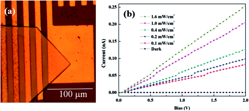 | ||
| Fig. 5 (a) A microscopic image of a (PEA)2PbBr4-based photodetector. (b) Current–voltage curves of the photodetector illuminated by a 405 nm laser. | ||
This resulted in the fabrication of arrayed (PEA)2PbBr4 photoconducting prototype devices based on (PEA)2PbBr4/Au Schottky contacts. The effective illumination area (active area) of our photodetector was estimated to be 2 × 10⁻³ cm2. The photodetector showed an effective photoresponse under ultraviolet 405 nm laser illumination, as shown in Fig. 5(b). The significantly low dark current was 5.56 × 10⁻¹³ A under a bias of 2.0 V. The on/off ratio was about 103 at a laser power intensity of 0.1 mW cm−2, which was similar to those reported recently for single crystalline photodetectors.40
Conclusions
In summary, we have grown centimeter-scale (PEA)2PbBr4 single crystals with a well-defined shape and large aspect ratio using a seeded method, and investigated their efficient photoresponse. This method could also be applied to other 2D perovskite materials to increase their lateral size to the wafer scale for integrated optoelectronic applications.Conflicts of interest
There are no conflicts of interest to declare.Acknowledgements
This work was financially supported by the National 973 program (No. 2013CB632105) and the National Natural Science Foundation of China (No. 11174018 and No. 61404003).Notes and references
- W. Nie, H. Tsai, R. Asadpour, J. C. Blancon, A. J. Neukirch, G. Gupta, J. J. Crochet, M. Chhowalla, S. Tretiak, M. A. Alam, H. L. Wang and A. D. Mohite, Science, 2015, 347, 522 CrossRef CAS PubMed.
- Y. H. Kim, H. Cho, J. H. Heo, T. S. Kim, N. Myoung, C. L. Lee, S. H. Im and T. W. Lee, Adv. Mater., 2015, 27, 1248 CrossRef CAS PubMed.
- G. C. Xing, N. Mathews, S. S. Lim, N. Yantara, X. F. Liu, D. Sabba, M. Grazel, S. Mhaisalkar and T. C. Sum, Nat. Mater., 2014, 13, 476 CrossRef CAS PubMed.
- Y. Lee, J. Kwon, E. Hwang, C. H. Ra, W. J. Yoo, J. H. Ahn, J. H. Park and J. H. Cho, Adv. Mater., 2015, 27, 41 CrossRef CAS PubMed.
- L. Dou, J. Mater. Chem. C, 2017, 5, 11165 RSC.
- R. Li, C. Yi, R. Ge, W. Zou, L. Cheng, N. Wang, J. Wang and W. Huang, Appl. Phys. Lett., 2016, 109, 151101 CrossRef.
- J. Chen, L. Gan, F. Zhuge, H. Li, J. Song, H. Zeng and T. Zhai, Angew. Chem., Int. Ed., 2017, 56, 2390 CrossRef CAS PubMed.
- B. Saparov and D. B. Mitzi, Chem. Rev., 2016, 116, 4558 CrossRef CAS PubMed.
- D. H. Cao, C. C. Stoumpos, O. K. Farha, J. T. Hupp and M. G. Kanatzidis, J. Am. Chem. Soc., 2015, 137, 7843 CrossRef CAS PubMed.
- D. B. Mitzi, M. T. Prikas and K. Chondroudis, Chem. Mater., 1999, 11, 542 CrossRef CAS.
- D. B. Mitzi, Chem. Mater., 2001, 13, 3283 CrossRef CAS.
- D. B. Mitzi, J. Chem. Soc., Dalton Trans., 2001, 1, 1 RSC.
- Z. Cheng and J. Lin, CrystEngComm, 2010, 12, 2646 RSC.
- D. Ma, Y. Fu, L. Dang, J. Zhai, I. A. Guzei and S. Jin, Nano Res., 2017, 10, 2117 CrossRef CAS.
- J. Ding and Q. Yan, Sci. China Mater., 2017, 60, 1063 CrossRef CAS.
- Y. Liu, Z. Yang and S. F. Liu, Adv. Sci., 2018, 5, 1700471 CrossRef PubMed.
- M. I. Saidaminov, A. L. Abdelhady, B. Murali, E. Alarousu, V. M. Burlakov, W. Peng, I. Dursun, L. Wang, Y. He, G. Maculan, A. Goriely, T. Wu, O. F. Mohammed and O. M. Bakr, Nat. Commun., 2015, 6, 7586 CrossRef PubMed.
- D. Shi, V. Adinolfi, R. Comin, M. Yuan, E. Alarousu, A. Buin, Y. Chen, S. Hoogland, A. Rothenberger, K. Katsiev, Y. Losovyj, X. Zhang, P. A. Dowben, O. F. Mohammed, E. H. Sargent and O. M. Bakr, Science, 2015, 347, 519 CrossRef CAS PubMed.
- Y. Dang, Y. Liu, Y. Sun, D. Yuan, X. Liu, W. Lu, G. Liu, H. Xia and X. Tao, CrystEngComm, 2015, 17, 665 RSC.
- Z. Lian, Q. Yan, Q. Lv, Y. Wang, L. Liu, L. Zhang, S. Pan, Q. Li, L. Wang and J. Sun, Sci. Rep., 2015, 5, 16563 CrossRef PubMed.
- Y. Liu, Z. Yang, D. Cui, X. Ren, J. Sun, X. Liu, J. Zhang, Q. Wei, H. Fan, F. Yu, X. Zhang, C. Zhao and S. F. Liu, Adv. Mater., 2015, 27, 5176 CrossRef CAS PubMed.
- Y. Liu, X. Ren, J. Zhang, Z. Yang, D. Yang, F. Yu, J. Sun, C. Zhao, Z. Yao, B. Wang, Q. Wei, F. Xiao, H. Fan, H. Deng, L. Deng and S. F. Liu, Sci. China: Chem., 2017, 60, 1367 CrossRef CAS.
- Y. Liu, J. Sun, Z. Yang, D. Yang, X. Ren, H. Xu, Z. Yang and S. F. Liu, Adv. Opt. Mater., 2016, 4, 1829 CrossRef CAS.
- Y. Liu, Y. Zhang, K. Zhao, Z. Yang, J. Feng, X. Zhang, K. Wang, L. Meng, H. Ye, M. Liu and S. F. Liu, Adv. Mater., 2018, 30, 1707314 CrossRef PubMed.
- Y. Liu, Y. Zhang, Z. Yang, D. Yang, X. Ren, L. Pang and S. F. Liu, Adv. Mater., 2016, 28, 9204 CrossRef CAS PubMed.
- Y. Chen, Q. Ge, Y. Shi, J. Liu, D. Xue, J. Ma, J. Ding, H. Yan, J. Hu and L. Wan, J. Am. Chem. Soc., 2016, 138, 16196 CrossRef CAS PubMed.
- H. Rao, W. Li, B. Chen, D. Kuang and C. Su, Adv. Mater., 2017, 29, 1602639 CrossRef PubMed.
- L. Lee, J. Baek, K. S. Park, Y. E. Lee, N. K. Shrestha and M. M. Sung, Nat. Commun., 2017, 8, 15882 CrossRef CAS PubMed.
- H. Rao, B. Chen, X. Wang, D. Kuang and C. Su, Chem. Commun., 2017, 53, 5163 RSC.
- J. Zhao, G. Kong, S. Chen, Q. Li, B. Huang, Z. Liu, X. San, Y. Wang, C. Wang, Y. Zhen, H. Wen, P. Gao and J. Li, Sci. Bull., 2017, 62, 1173 CrossRef CAS.
- T. Geske, J. Li, M. Worden, X. Shan, M. Chen, S. G. R. Bade and Z. Yu, Adv. Funct. Mater., 2017, 27, 1702180 CrossRef.
- C. Fang, J. Li, J. Wang, R. Chen, H. Wang, S. Lan, Y. Xuan, H. Luo, P. Fei and D. Li, CrystEngComm, 2018, 20, 6538 RSC.
- L. Dou, A. B. Wong, Y. Yu, M. Lai, N. Kornienko, S. W. Eaton, A. Fu, C. G. Bischak, J. Ma, T. Ding, N. S. Ginsberg, L. Wang, A. P. Alivisatos and P. Yang, Science, 2015, 349, 1518 CrossRef CAS PubMed.
- D. Liang, Y. Peng, Y. Fu, M. J. Shearer, J. Zhang, J. Zhai, Y. Zhang, R. J. Hamers, T. L. Andrew and S. Jin, ACS Nano, 2016, 10, 6897 CrossRef CAS PubMed.
- S. Yang, W. Niu, A. Wang, Z. Fan, B. Chen, C. Tan, Q. Lu and H. Zhang, Angew. Chem., Int. Ed., 2017, 56, 4252 CrossRef CAS PubMed.
- W. Peng, J. Yin, K. Ho, O. Ouellette, M. D. Bastiani, B. Murali, O. E. Tall, C. Shen, X. Miao, J. Pan, E. Alarousu, J. H. He, B. S. Ooi, O. F. Mohammed, E. Sargent and O. M. Bakr, Nano Lett., 2017, 17, 4759 CrossRef CAS PubMed.
- W. Zhai, C. Ge, X. Fang, K. Zhang, C. Tian, K. Yuan, S. Sun, Y. Li, W. Chen and G. Ran, RSC Adv., 2018, 8, 14527 RSC.
- F. Lédée, G. T. Allard, H. Diab, P. Audebert, D. Garrot, J. S. Lauret and E. Deleporte, CrystEngComm, 2017, 19, 2598 RSC.
- K. Wang, C. Wu, D. Yang, Y. Jiang and S. Priya, ACS Nano, 2018, 12, 4919 CrossRef CAS PubMed.
- Y. Zhang, Y. Liu, Z. Xu, H. Ye, Q. Li, M. Hu, Z. Yang and S. F. Liu, J. Mater. Chem. C, 2019, 7, 1584 RSC.
- Z. Yang, Y. Deng, X. Zhang, S. Wang, H. Chen, S. Yang, J. Khurgin, N. X. Fang, X. Zhang and R. Ma, Adv. Mater., 2018, 30, 1704333 CrossRef PubMed.
- N. Kawano, M. Koshimizu, Y. Sun, N. Yahaba, Y. Fujimoto, T. Yanagida and K. Asia, J. Phys. Chem. C, 2014, 118, 9101 CrossRef CAS.
- H. Takagi, H. Kunugita and K. Ema, Phys. Rev. B: Condens. Matter Mater. Phys., 2013, 87, 125421 CrossRef.
- D. W. deQuilettes, S. M. Vorpahl, S. D. Stranks, H. Nagaoka, G. E. Eperon, M. E. Ziffer, H. J. Snaith and D. S. Ginger, Science, 2015, 348, 683 CrossRef CAS PubMed.
- L. Gan, J. Li, Z. Fang, H. He and Z. Ye, J. Phys. Chem. Lett., 2017, 8, 5177 CrossRef PubMed.
Footnote |
| † Electronic supplementary information (ESI) available. See DOI: 10.1039/c9ra01415b |
| This journal is © The Royal Society of Chemistry 2019 |

