
 Open Access Article
 This Open Access Article is licensed under a Creative Commons Attribution-Non Commercial 3.0 Unported Licence
Improvement of perovskite crystallinity by omnidirectional heat transfer via radiative thermal annealing†
Jiyoon Park‡
a,
Jin Woo Choi‡ b,
Woochul Kima,
Ryeri Leea,
Hee Chul Woob,
Jisoo Shinb,
Hyeonghun Kima,
Yeong Jun Sona,
Ji Young Joa,
Heon Leec,
Sooncheol Kwond,
Chang-Lyoul Lee*b and
Gun Young Jung*a
b,
Woochul Kima,
Ryeri Leea,
Hee Chul Woob,
Jisoo Shinb,
Hyeonghun Kima,
Yeong Jun Sona,
Ji Young Joa,
Heon Leec,
Sooncheol Kwond,
Chang-Lyoul Lee*b and
Gun Young Jung*a
aSchool of Materials Science and Engineering (SMSE), Gwangju Institute of Science and Technology (GIST), 123 Cheomdangwagi-ro, Buk-gu, Gwangju 61005, Republic of Korea. E-mail: gyjung@gist.ac.kr
bAdvanced Photonics Research Institute (APRI), Gwangju Institute of Science and Technology (GIST), 123 Cheomdangwagi-ro, Buk-gu, Gwangju 61005, Republic of Korea. E-mail: vsepr@gist.ac.kr
cDepartment of Materials Science and Engineering, Korea University, Seoul 02841, Republic of Korea
dResearch Institute of Solar and Sustainable Energies (RISE), Gwangju Institute of Science and Technology (GIST), 123 Cheomdangwagi-ro, Buk-gu, Gwangju 61005, Republic of Korea
First published on 14th May 2019
Abstract
As promising photo-absorbing materials for photovoltaics, organic–inorganic hybrid perovskite materials such as methylammonium lead iodide and formamidinium lead iodide, have attracted lots of attention from many researchers. Among the various factors to be considered for high power conversion efficiency (PCE) in perovskite solar cells (PSCs), increasing the grain size of perovskite is most important. However, it is difficult to obtain a highly crystalline perovskite film with large grain size by using the conventional hot-plate annealing method because heat is transferred unidirectionally from the bottom to the top. In this work, we presented radiative thermal annealing (RTA) to improve the structural and electrical properties of perovskite films. Owing to the omnidirectional heat transfer, swift and uniform nuclei formation was possible within the perovskite film. An average grain size of 500 nm was obtained, which is 5 times larger than that of the perovskite film annealed on a hot-plate. This perovskite film led to an enhancement of photovoltaic performance of PSCs. Both short-circuit current density and PCE of the PSCs prepared by RTA were improved by 10%, compared to those of PSCs prepared by hot-plate annealing.
1. Introduction
Solar energy is considered an eco-friendly next-generation renewable energy. Among the various types of solar cells, perovskite solar cells (PSCs) have attracted considerable attention over the past decade due to their outstanding optical and electrical properties, such as high light absorption coefficient in the visible range, low exciton binding energy under 50 meV, high ambipolar charge mobility as well as solution processability.1–9 The power conversion efficiency (PCE) of PSCs has been dramatically enhanced, reaching ∼22%. Furthermore, the PCE of PSCs is expected to surpass that of silicon solar cells within 10 years.10–17Several factors, such as halide composition control for band-gap tuning of the perovskite photo-active layer,18 high crystallinity of the perovskite film with large grain size19 and optimization of energy band alignment in the device structure,20 must be improved to the satisfactory level to realize high PCE in PSCs. Among these factors, the crystallinity and grain size of perovskite, which are strongly related to exciton dissociation,21 charge transport22–24 and extraction efficiency,25,26 are extremely important to enhance the photovoltaic performance of PSCs. High crystallinity in a perovskite film signifies a low density of defects with less grain boundaries (GBs). It suppresses the energy band distortion induced by GBs of the perovskite film,27 resulting in efficient exciton dissociation by minimizing carrier recombination at the GBs. Perovskite films with larger grains have less GBs, which improve their charge transport and extraction efficiency26 by suppressing charge recombination and trapping.19
To realize a highly crystalline perovskite film with large grain size, various methods have been reported, including one-step spin-coating with anti-solvent dripping,28,29 deposition by an evaporation method under vacuum conditions13,30 and blade coating.31 In addition, control of the crystallinity and grain size of perovskite film through various post-annealing methods has been investigated.32,33 In general, as-deposited perovskite films are subsequently annealed on a hot-plate to form the crystalline perovskite by evaporating the solvent.10–17 However, this method has a critical limitation of unidirectional heat transfer from the bottom; the annealing temperature is inhomogeneous between the top and bottom sides of the perovskite film. Due to the lack of uniform heat distribution within the perovskite film, the hot-plate annealing method yields perovskite films with inferior crystallinity and smaller grain size compared to the other reported annealing methods and suffers from poor reproducibility. Therefore, there is a great need to develop new post-annealing methods to replace the hot-plate annealing method for obtaining highly crystalline perovskite films with large grains.
Recently, two research groups reported new post-annealing methods using a light as an energy source and non-direct thermal heating; Jeon et al. introduced a near-infrared (NIR) laser annealing method and obtained a large grain size (∼300 nm) in perovskite film.32 F. Huang et al. reported a dual-flash annealing process, in which the perovskite film was treated via a 2-step annealing process involving a low-pressure flash evaporation stage followed by a high-temperature flash annealing step.33 The PSCs based on these films exhibited enhanced photovoltaic (PV) performances (∼19%). Although the abovementioned methods are significant for improving the crystallinity along with large grain size, there are limitations, such as long processing time and expensive equipment.
In addition, many studies have also been reported on annealing for as-deposited perovskite films by using rapid thermal annealing techniques. In general, the rapid thermal annealing methods have been widely used to improve the structural and electrical properties of semiconducting materials.34,35 These techniques can raise the temperature rapidly by using various heating sources such as intense pulsed light,32,36 flash light,33 infrared (IR) radiation,37,38 etc. Among them, the radiative annealing using the IR lamp is advantageous for transferring the heat omnidirectionally, allowing uniform heat distribution within the thin films but, it was barely used in PSCs. V. L. Pool et al. utilized the radiative thermal annealing (hereafter abbreviated as RTA) technique in perovskite film annealing stage to explain the decomposition kinetics of FAPbI3 depending on the RTA temperature and heating time.37 B. Dou et al. also used the RTA method for annealing as-deposited perovskite films to see the effect of processing conditions, i.e. anti-solvent, humidity, and annealing conditions, on the film quality of MAPbI3 through in situ XRD analysis.38
In this study, we applied a radiative thermal annealing (RTA) to improve the crystallinity and grain size of perovskite films. Differences in crystallinity and grain size of the perovskite films prepared by these two different post-annealing methods (RTA vs. hot plate annealing) and their effects on the device performance of PSCs were investigated. 20 PSCs were fabricated by each method and their PV performances were statistically characterized. In addition, the interfacial and optical (exciton) characteristics of perovskite films, such as charge transport, exciton binding energy and charge dissociation, were also investigated to verify the origin for the enhanced PV performance by the RTA.
2. Experimental section
2.1 Fabrication of perovskite solar cells using the RTA-perovskite
A fluorine-doped tin oxide (FTO) substrate was cleaned for 15 min in sequence of acetone, isopropyl alcohol, deionized water and dried using a nitrogen gun. The substrate was further cleaned by UV–ozone for 15 min. After UV–ozone treatment, a compact TiO2 layer acting as a hole blocker was deposited onto the cleaned FTO substrate by spin-coating a TiO2 stock solution of 0.15 M titanium butoxide in 1-butanol at 2000 rpm for 40 s. After spin-coating, the substrate was dried on a hot-plate at 125 °C for 5 min to remove the residual solvent. Then, the substrate was annealed at 550 °C for 30 min in a furnace to transform the TiO2 phase from rutile to anatase. The mesoporous TiO2 layer as an electron-transport layer (ETL) was formed by spin-coating a TiO2 paste, which was composed of 30 nm nanoparticles (NPs) in 2-methoxyethanol (1![[thin space (1/6-em)]](https://www.rsc.org/images/entities/char_2009.gif) :5 weight ratio), at 4000 rpm for 15 s onto the TiO2 blocking layer. The sample was dried at 125 °C for 5 min and then annealed at 550 °C for 1 h to burn out the polymer ligands wrapping around the TiO2 NPs.
:5 weight ratio), at 4000 rpm for 15 s onto the TiO2 blocking layer. The sample was dried at 125 °C for 5 min and then annealed at 550 °C for 1 h to burn out the polymer ligands wrapping around the TiO2 NPs.
The perovskite precursor solution was prepared by mixing 1.2 M PbI2 (99%, TCI), 1.02 M methylammonium iodide (MAI, 98%, Sigma Aldrich), 0.18 M formamidinium iodide (FAI, 99%, TCI) and 1.2 M DMSO (99%, Sigma Aldrich) in DMF (99%, Sigma Aldrich). The solution was then stirred at room temperature for 6 h. An approximately 300 nm-thick (MAPbI3)0.85(FAPbI3)0.15 layer was deposited by spin-coating the precursor solution at 3500 rpm for 40 s. Just before spin-coating was finished, 80 μL of toluene was dropped to instantaneously remove the DMF within the perovskite film. The as-deposited perovskite films were annealed in a radiative thermal annealing (RTA) system under N2 atmosphere. Fig. S1a (ESI†) shows the schematic presentation of the RTA steps. Chamber was heated up to 120 °C for 30 s with a ramping rate of 4 °C s−1. After reaching the set temperature, the film was annealed at 120 °C for 10 min. A spiro-OMeTAD layer as a hole-transport layer (HTL) was deposited onto the perovskite layer by spin-coating at 2000 rpm for 20 s. The spiro-OMeTAD solution was prepared by dissolving 72.3 mg of spiro-OMeTAD in 1 mL of chlorobenzene and then adding 28.8 μL of 4-tert-butylpyridine and 17.5 μL of a stock solution of lithium bis(trifluoromethylsulfonyl)imide (Li-TFSI 520 mg in 1 mL of acetonitrile). After spin-coating the HTL, the samples were stored in a desiccator for 24 h to oxidize the spiro-OMeTAD for improving the hole extraction and transport properties.39 Finally, an 80 nm-thick gold electrode was deposited by thermal evaporation. All processes for PSCs fabrication were performed in a glove box filled with high purity N2 gas except when transporting the sample to RTA apparatus. All procedures are illustrated in Fig. S1b (ESI†). A schematic and a cross-sectional scanning electron microscopy image of a perovskite solar cell are shown in Fig. S1c and S1d (ESI†).
2.2 Crystal structure and morphology characterization of perovskite films
The crystalline phase of perovskite films was characterized by X-ray diffraction (XRD) using a CuKα radiation source (40 kV, 40 mA, Advanced D8, Bruker, Germany). The surface crystalline phase of perovskite film was analyzed by grazing incidence XRD (GIXRD) using above mentioned XRD equipment. In GIXRD measurements, the incidence angle of X-ray was 0.1°. The morphology of the perovskite films was observed with field-emission scanning electron microscopy (FE-SEM, JEOL 2020F) with an accelerating voltage of 10 keV.2.3 Measurements
3. Result and discussion
In general, X-ray diffraction (XRD) patterns are utilized to analyze the crystalline structure and degree of crystallinity of films. Fig. 1 shows the crystallographic characterization of perovskite films prepared by two different post-annealing methods. To precisely compare the effect of each annealing method on the crystallographic property, optimization of two post-annealing processes was first conducted. As several research groups reported that heat treatment at 120 °C is the optimum condition for post-annealing of perovskite films on a hot-plate (HPA-perovskite),40–43 we also fixed the annealing temperature at 120 °C for the radiative thermal annealing process (RTA-perovskite) so that we can carry out direct comparison. In the post-annealing process using a hot-plate, the annealing temperature and time were fixed at 120 °C and 10 min, respectively, in accordance with the references. 40–43 Top-view scanning electron microscopy (SEM) images of perovskite films at various RTA times (from 1 min to 20 min) and their corresponding XRD patterns are shown in Fig. S2a and S2b (ESI†). There was no significant difference in the SEM images with increasing the RTA time; however, the XRD results showed a considerable difference. After 10 min of post-annealing, a new diffraction peak emerged at 12.7°, corresponding to the (001) plane of PbI2.44 The intensity of PbI2 peak increased with increasing the RTA time. It was previously reported that a small amount of PbI2 can act as a passivation layer to prevent recombination at the interface between the perovskite and the hole-transport layer (HTL),45,46 which could contribute to improve the short-circuit current density (Jsc) in the PSCs. However, excess PbI2 has adverse effects on the photovoltaic (PV) performances of PSCs when annealed for more than 10 min, which will be explained in more detail in the device performance section. Based on the SEM and XRD results shown in Fig. S2a and S2b (ESI†), annealing at 120 °C for 10 min was chosen as the optimum condition for the RTA-perovskite. The PV parameters and their statistical distribution depending on the RTA time are shown in Table S1 and Fig. S2c (ESI).†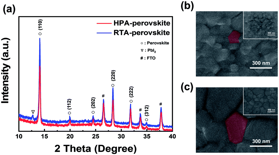 | ||
| Fig. 1 Structural characterization of perovskite films prepared by two different annealing methods. (a) XRD patterns of two perovskite films prepared by two different post-annealing processes. Top-view FE-SEM images of (b) HPA-perovskite film and (c) RTA-perovskite film. The red-colored area represents one grain and the inset image is low-magnified FE-SEM image. | ||
Fig. 1a shows XRD patterns of perovskite films annealed by two different methods. The prominent XRD peaks in both films appeared at 14.08° and 28.38°, corresponding to the (110) and (220) planes of the perovskite, respectively.44 Compared to those in HPA-perovskite, the intensity of main (110) peak at 14.08° in RTA-perovskite was higher and the full-width at half-maximum (FWHM) value was smaller, indicating that the crystallinity of the RTA-perovskite was better than that of the HPA-perovskite. Interestingly, there was no PbI2 diffraction peak at 12.7° in the HPA-perovskite. We assumed that it resulted from the difference in heat transfer mechanisms between hot plate annealing and RTA system. In hot plate annealing system, the perovskite film received less energy from the heating source since the heat travelled through glass, fluorine-doped tin oxide (FTO), electron transporting layer (ETL) to reach the perovskite film. However, in RTA system, since the heat was transferred directly to the perovskite film, it received all energy from the heating source without any loss.38 As a result, we predict that the degree of methylammonium iodide (MAI) decomposition is different between hot plate annealing and RTA system, resulting in the formation of a small amount PbI2 only in RTA. Fig. 1b and c compare top-view SEM images of perovskite films prepared by two different post-annealing methods. The insets are low magnification SEM images of both perovskite films. The average grain size of RTA-perovskite was measured as approximately 500 nm, however, sub-100 nm grains were observed in the HPA-perovskite.
The grain size difference between the RTA- and HPA-perovskite was resulted from the difference in nucleation rate by heat transfer mechanism.47 In general, the grains are developed through three steps; (i) nucleation, (ii) subsequent crystal growth at the nucleus and (iii) merging of neighboring crystals. Of these steps, the nucleation process occurs when the embryo overcomes its activation energy (ΔG) for making nuclei.48 In the hot plate-annealing, the temperature gradient occurred within the as-deposited perovskite film since the thermal energy was delivered from the bottom to upper layer by unidirectional heat transfer via conduction (left scheme in Fig. 2a). Thus, the nuclei were initially formed only at the bottom side of perovskite film. Consequentially, a relatively longer time was required for nucleation in the whole perovskite film. Therefore, it shortened the time for the growth of crystals and their merging into grains during the limited annealing time, resulting in a smaller grain size.
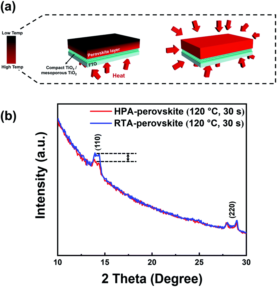 | ||
| Fig. 2 Scheme of heat transfer mechanism in each annealing method and the analysis of perovskite film at the surface region. (a) Illustration of heat transfer mechanism within the perovskite film via the hot-plate (left side) or RTA (right side) post annealing process. The red arrows indicate the heat transfer direction. (b) GIXRD patterns of two perovskite films prepared by different post-annealing processes. The films were annealed at 120 °C for only 30 s. | ||
Besides, the movement of precursor ions was largely dependent on their position within the as-deposited perovskite film due to the unidirectional heat transfer from bottom side. Compared to the bottom part of perovskite film, which received huge amount of thermal energy from hot-plate via conduction, the movement of precursor ions at the top side was relatively suppressed due to the less thermal energy. It reduced the chance of the precursor ions sticking to the embryos, rendering less chance for nuclei formation. Therefore, this thermal energy distribution within the film induced uneven nuclei formation and accordingly grain growth with different sizes along the thickness of perovskite film.47 These phenomena including slow nucleation and suppressed migration of ions generated perovskite grains of sub-100 nm size by hot-plate annealing (Fig. 1b).
However, in the RTA process, thermal energy distribution within the as-deposited perovskite film was much uniform than that of the hot-plate annealing process owing to the omnidirectional heat transfer via radiation (right scheme in Fig. 2a). Active movement of precursor ions produced uniform nuclei in a relatively short time within the as-deposited perovskite film regardless of the position. Therefore, more thermal energy can be used up for the crystal growth and their merging into a grain in the same annealing time, inducing larger perovskite grains of approximately 500 nm size (Fig. 1c).
To further check the nucleation and grain growth at the film surface in initial annealing state of RTA process, grazing-incidence XRD (GIXRD) measurements were conducted with the HPA- and RTA-treated films with an incidence angle of 0.1°. In general, as the GIXRD uses a small incidence angle for incoming X-ray, the penetration depth of X-ray is limited to the surface and most scattering signals mainly comes from it.49 The heat treatment of perovskite films was performed for only 30 s to check the initial nuclei creation at the surface region. Fig. 2b shows the GIXRD patterns of HPA- and RTA-perovskite in initial annealing stage. The intensity of (110) main peak of RTA-perovskite was higher than that of HPA-perovskite, demonstrating that crystallization process including nucleation and crystal growth occurred more actively at the surface by the RTA. The swift nucleation and crystal growth consequentially contributed to larger grains.
Fig. 3 shows the PV performances of PSCs. Fig. 3a compares representative current density–voltage (J–V) curves, external quantum efficiency (EQE) spectra and the corresponding integrated current density of the PSCs produced by two different post-annealing methods. The best and average PV parameters, including the open-circuit voltage (Voc), short-circuit current density (Jsc), fill factor (FF) and PCE, are listed in Table 1. The PSCs using the HPA-perovskite (HPA-PSCs) demonstrated average PV parameter values, which were obtained from 20 PSCs (the histograms of Jsc and PCE are shown in Fig. 3b); Voc of 1.04 V, Jsc of 20.26 mA cm−2, FF of 0.65 and PCE of 13.74%. In comparison, the PSCs using RTA-perovskite (RTA-PSCs) demonstrated enhanced PV performances with a Voc of 1.06 V, a Jsc of 21.94 mA cm−2, a FF of 0.67, a PCE of 15.49% and improved EQE in visible wavelengths. As explained earlier, the small amount of PbI2 acted as a passivation layer, contributing to the improvement in Jsc in the RTA-PSCs. Compared with the HPA-PSCs, both Jsc and PCE were enhanced by 10%. In addition, the RTA-PSCs demonstrated a lower series resistance of 99.479 Ω than the HPA-PSCs (106.679 Ω) measured under illumination conditions, suggesting that the high crystallinity and large perovskite grains allowed the transport of photogenerated carriers with minimal energy loss along the interfaces, which is advantageous for the higher FF.
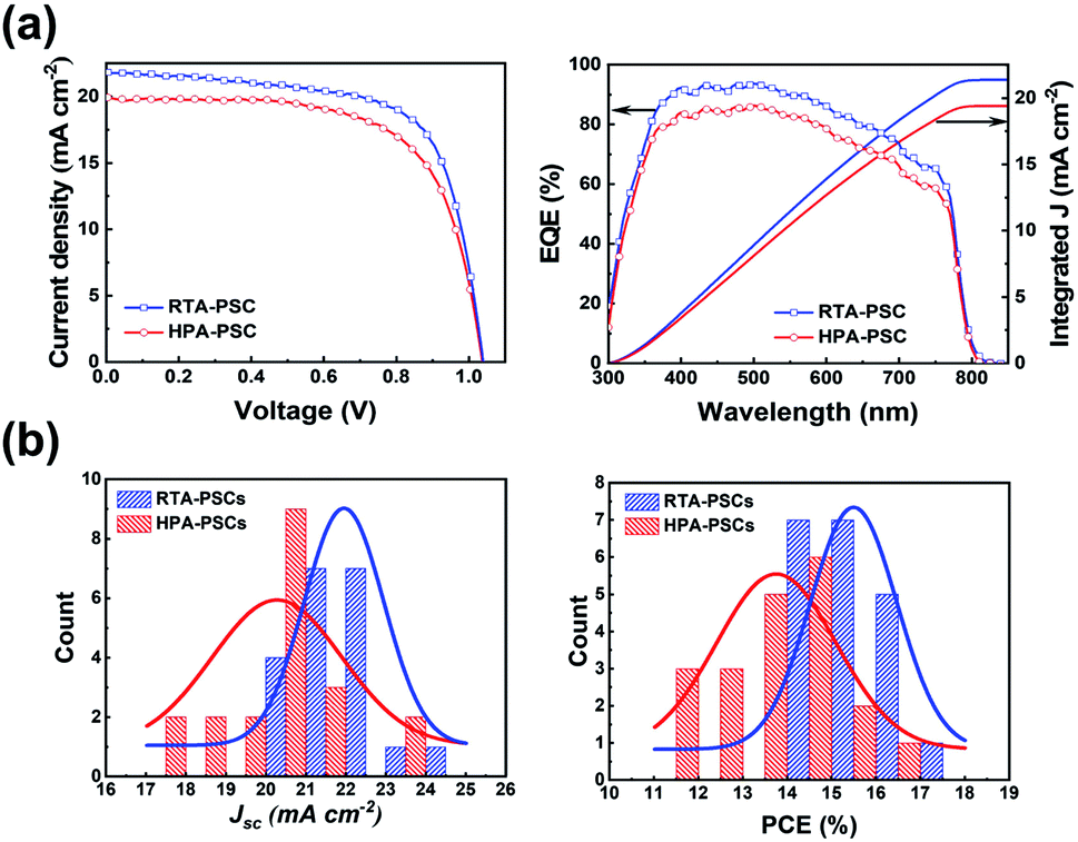 | ||
| Fig. 3 (a) Representative PV performances of the PSCs prepared by two different post-annealing methods; J–V curves, EQE spectra, and corresponding integrated current density. (b) Histograms of the Jsc and PCE from the 20 PSCs in each annealing method. | ||
| Voc (V) | Jsc (mA cm−2) | FF | Rs (Ω) | PCE (%) | |
|---|---|---|---|---|---|
| HPA-PSCs | 1.04 (1.04 ± 0.03) | 23.20 (20.26 ± 1.58) | 0.67 (0.65 ± 0.03) | 106.68 | 16.02 (13.74 ± 1.31) |
| RTA-PSCs | 1.06 (1.06 ± 0.02) | 24.33 (21.94 ± 0.97) | 0.68 (0.67 ± 0.02) | 99.48 | 17.37 (15.49 ± 0.95) |
The interfacial characteristics of the two PSCs prepared by different post-annealing methods were investigated by electrochemical impedance spectroscopy (EIS). EIS was performed at Voc of each PSC under dark. Fig. 4a and b show the Nyquist plots with the equivalent circuit model for interpreting EIS data. The equivalent circuit is shown in the inset of Fig. 4b. The Nyquist plot is comprised of two semi-circles; the large semi-circle in the low-frequency region below 10 kHz and the small semi-circle in the high-frequency region above 10 kHz. The large semi-circle in Fig. 4a is associated with the recombination resistance. Meanwhile, the small semi-circle magnified in Fig. 4b relates to the charge-transport resistance.50,51 Herein, Rc represents the contact resistance between the FTO electrode and counter electrode, Rrec and Rct are defined as the recombination resistance and charge transport resistance at the interfaces, respectively. The values of Rc, Rrec and Rct are summarized in Table 2. The Rrec measured in the RTA-PSCs (312 Ω) was higher than that measured in the HPA-PSCs (166 Ω). On the other hand, the RTA-PSCs had a lower Rct (32.5 Ω) compared to the HPA-PSCs (37.6 Ω). The higher Rrec and lower Rct of the RTA-PSCs suggested that charge recombination was greatly suppressed at the interfaces of the HTL and/or electron-transport layer (ETL) with the perovskite film.
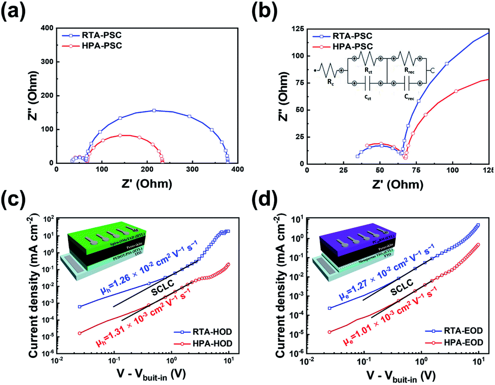 | ||
| Fig. 4 (a) Nyquist plots of PSCs prepared by two different post-annealing methods. The radius of large semi-circle in the low-frequency region indicates the recombination resistance at the interfaces within the PSC. (b) The magnified Nyquist plots in the high-frequency region; the radius of small semi-circle indicates the charge transport resistance at the interfaces within the PSC. The inset represents the equivalent circuit utilized to fit the Nyquist plots. J–V characteristics of (c) hole-only device and (d) electron-only device. Charge carrier mobility of perovskite film was calculated by fitting the space-charge limited current (SCLC) region with Mott–Gurney law. The device structures of hole-only device and electron-only device are drawn in each graph. | ||
| HPA-perovskite | RTA-perovskite | |
|---|---|---|
| Contact resistance, Rc (Ω) | 30.1 | 33.0 |
| Recombination resistance, Rrec (Ω) | 166 | 312 |
| Charge transport resistance, Rct (Ω) | 37.6 | 32.5 |
Hole and electron mobilities of the two perovskite films were measured with the hole- and electron-only devices; ITO/PEDOT:PSS/perovskite/spiro-OMeTAD/Ag and fluorine-doped tin oxide (FTO)/TiO2 blocking layer/mesoporous TiO2 (mp-TiO2)/perovskite/PC60BM/Al, respectively. The hole and electron mobilities can be calculated in the SCLC regime, where the current depends on only the charge carrier mobility and J–V characteristics become quadratic, following the Mott–Gurney law:
 | (1) |
The photocurrent of PSCs strongly depends on the exciton dissociation efficiency in the perovskite film and this exciton dissociation efficiency is determined by the exciton binding energy. Fig. 5 shows the integrated photoluminescence (PL) intensity of HPA- and RTA-perovskite films at the temperatures from 60 K to 200 K, which were integrated from the PL spectra in Fig. S3 (ESI†). The exciton binding energy of perovskite film can be estimated by fitting temperature-dependent integrated PL intensity with following Arrhenius equation:
 | (2) |
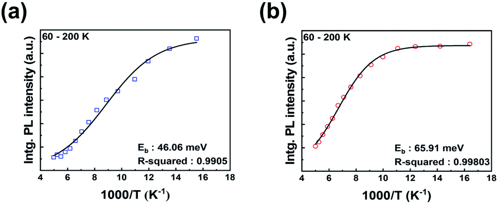 | ||
| Fig. 5 Temperature dependence of integrated PL intensity of perovskite films; (a) RTA-perovskite and (b) HPA-perovskite. The lines are fitted by Arrhenius equation. | ||
The transient PL characteristics of perovskite films were also measured to evaluate the exciton dissociation efficiency. The PL decay curves (Fig. 6) were monitored at 775 nm, which is the PL emission peak of perovskite film (inset of Fig. 6). The PL decay curves were fitted by bi-exponential function to extract the lifetimes (τ) and fractional intensities (f) for fast-decay (τ1, f1) and slow-decay (τ2, f2) components and the intensity-weighted average exciton lifetime (τave) (see Table 3). Compared to the τave (226 ns) of HPA-perovskite, the τave of RTA-perovskite was significantly shortened to 136 ns, implying that the generated excitons were efficiently dissociated in the RTA-perovskite, enabling more electrons to contribute to external current in PSCs. The excitons with less binding energy can dissociate efficiently, resulting in a short exciton lifetime.
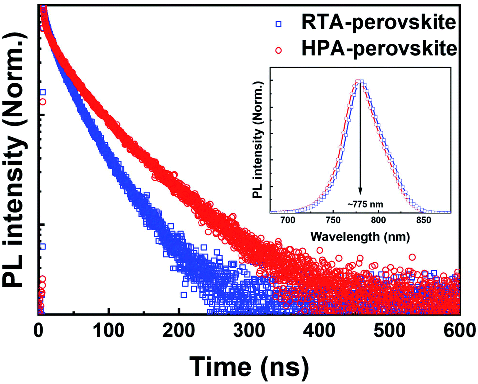 | ||
| Fig. 6 Time-resolved PL decay curves of the RTA-perovskite and HPA-perovskite prepared on a mp-TiO2/glass substrate. The inset shows the steady-state PL spectra. | ||
| τ1 (f1) (ns) | τ2 (f2) (ns) | χ2 | τave (ns) | |
|---|---|---|---|---|
| a The monitored PL emission peak of both perovskite films was λ = 775 nm. The PL decay curves were fitted with a bi-exponential function to calculate the lifetime of perovskite. χ2 is the reduced chi-squared value. Intensity-weighted average lifetime (τave) is defined as f1τ1 + f2τ2, in which f1 and f2 are fractional intensities and τ1 and τ2 are lifetimes. | ||||
| HPA-PSCs | 74 (0.23) | 271 (0.77) | 1.146 | 226 |
| RTA-PSCs | 55 (0.30) | 170 (0.70) | 1.106 | 136 |
4. Conclusions
The perovskite film annealed at 120 °C for 10 min by RTA revealed high crystallinity with a larger grain size of 500 nm. The electrochemical impedance spectroscopy (EIS) and space-charge limited current (SCLC) measurements confirmed higher recombination resistance, lower charge transport resistance and higher hole and electron mobilities in RTA-PSCs compared to the HPA-PSCs. In addition, a lower exciton binding energy and short exciton lifetime were also achieved from the perovskite film prepared by RTA. Thereby, the PSCs with the RTA-perovskite film demonstrated enhanced Jsc and PCE by 10%, compared to the HPA-perovskite PSCs. This study provides a simple method for achieving perovskite films with high crystallinity and large grain size for realizing highly efficient PSCs.Conflicts of interest
There are no conflicts to declare.Acknowledgements
This work was supported by the Pioneer Research Center Program (NRF-2016M3C1A3908893, NRF-2014M3C1A3016468) and by the Basic Science Research Program (NRF-2016R1A2B4006395) through the National Research Foundation of Korea (NRF) funded by the Ministry of Education. G. Y. Jung was partially supported by the GIST Research Institute (GRI) project through a grant provided by GIST in 2018. C.-L. Lee thanks the National Research Foundation of Korea (NRF) for financial support through a grant funded by the Korean government (MSIP; NRF-2016R1A2B4013003 and NRF-2018R1A2A3075144) and a grant funded by GIST 2019 (Research on Advanced Optical Science and Technology).Notes and references
- N. J. Jeon, J. H. Noh, W. S. Yang, Y. C. Kim, S. Ryu, J. Seo and S. I. Seok, Nature, 2015, 517, 476 CrossRef CAS PubMed.
- J.-H. Im, C. R. Lee, J.-W. Lee, S. W. Park and N. G. Park, Nanoscale, 2011, 3, 4088 RSC.
- N. G. Park, J. Phys. Chem. Lett., 2015, 4, 2423 CrossRef.
- N. G. Park, Nano Convergence, 2016, 3, 15 CrossRef PubMed.
- E. Mosconi, A. Amat, M. K. Nazeeruddin, M. Gratzel and F. D. Angelis, J. Phys. Chem. C, 2013, 117, 13902 CrossRef CAS.
- G. Xing, N. Mathews, S. Sun, S. S. Lim, Y. M. Lam, M. Gratzel, S. Mhaisalkar and T. C. Sum, Science, 2013, 342, 344 CrossRef CAS PubMed.
- H. Kim, K.-G. Lim and T.-W. Lee, Energy Environ. Sci., 2016, 9, 12 RSC.
- J. H. Heo, D. H. Song, H. J. Han, S. Y. Kim, J. H. Kim, D. Kim, H. W. Shin, T. K. Ahn, C. Wolf, T.-W. Lee and S. H. Im, Adv. Mater., 2015, 27, 3424 CrossRef CAS PubMed.
- B. Jeong, S. M. Cho, S. H. Cho, J. H. Lee, I. Hwang, S. K. Hwang, J. Cho, T.-W. Lee and C. Park, Phys. Status Solidi RRL, 2016, 10, 381 CrossRef CAS.
- A. Kojima, K. Teshima, Y. Shirai and T. Miyasaka, J. Am. Chem. Soc., 2009, 131, 6050 CrossRef CAS PubMed.
- H.-S. Kim, C.-R. Lee, J.-H. Im, K.-B. Lee, T. Moehl, A. Marchioro, S.-J. Moon, R. Humphry-Baker, J.-H. Yum, J. E. Moser, M. Gratzel and N.-G. Park, Sci. Rep., 2012, 2, 591 CrossRef PubMed.
- M. M. Lee, J. Teuscher, T. Miyasaka, T. N. Murakami and H. J. Snaith, Science, 2012, 338, 643 CrossRef CAS PubMed.
- M. Liu, M. B. Johnston and H. J. Snaith, Nature, 2013, 501, 395 CrossRef CAS PubMed.
- T. Leijtens, B. Lauber, G. E. Eperon, S. D. Stranks and H. J. Snaith, J. Phys. Chem. Lett., 2014, 5, 1096 CrossRef CAS PubMed.
- Z. Xiao, C. Bi, Y. Shao, Q. Dong, Q. Wang, Y. Yuan, C. Wang, Y. Gao and J. Huang, Energy Environ. Sci., 2014, 7, 2619 RSC.
- W. S. Yang, J. H. Noh, N. J. Jeon, Y. C. Kim, S. Ryu, J. Seo and S. I. Seok, Science, 2015, 348, 1234 CrossRef CAS PubMed.
- W. S. Yang, B.-W. Park, E. H. Jung, N. J. Jeon, Y. C. Kim, D. U. Lee, S. S. Shin, J. Seo, E. K. Kim, J. H. Noh and S. I. Seok, Science, 2017, 356, 1376 CrossRef CAS PubMed.
- J. H. Noh, S. H. Im, J. H. Heo, T. N. Mandal and S. I. Seok, Nano Lett., 2013, 13, 1764 CrossRef CAS PubMed.
- W. Nie, H. Tsai, R. Asadpour, J.-C. Blancon, A. J. Neukirch, G. Gupta, J. J. Crochet, M. Chhowalla, S. Tretiak, M. A. Alam, H.-L. Wang and A. D. Mohite, Science, 2015, 347, 522 CrossRef CAS PubMed.
- F. Giordano, A. Abate, J. P. C. Baena, M. Saliba, T. Matsui, S. H. Im, S. M. Zakeeruddin, M. K. Nazeeruddin, A. Hagfeldt and M. Gratzel, Nat. Commun., 2016, 7, 10379 CrossRef CAS PubMed.
- A. Miyate, A. Mitioglu, P. Plochocka, O. Portugall, J. T.-W. Wang, S. D. Strank, H. J. Snaith and R. J. Nicholas, Nat. Phys., 2015, 11, 582 Search PubMed.
- G. Horowitz and M. E. Hajlaoui, Adv. Mater., 2000, 12, 1046 CrossRef CAS.
- Y. Zhao, A. M. Nardes and K. Zhu, J. Phys. Chem. Lett., 2014, 5, 490 CrossRef CAS PubMed.
- L. Zheng, Y. Ma, S. Chu, S. Wang, B. Qu, L. Xiao, Z. Chen, Q. Gong, Z. Wu and X. Hou, Nanoscale, 2014, 6, 8171 RSC.
- J.-H. Im, I.-H. Jang, N. Pellet, M. Gratzel and N.-G. Park, Nat. Nanotechnol., 2014, 9, 927 CrossRef CAS PubMed.
- Z. Xiao, Q. Dong, C. Bi, Y. Shao, Y. Yuan and J. Huang, Adv. Mater., 2014, 26, 6503 CrossRef CAS PubMed.
- J.-J. Li, J.-Y. Ma, Q.-Q. Ge, J.-S. Hu, D. Wang and L.-J. Wan, ACS Appl. Mater. Interfaces, 2015, 7, 28518 CrossRef CAS PubMed.
- N. J. Jeon, J. H. Noh, Y. C. Kim, W. S. Yang, S. Ryu and S. I. Seok, Nat. Mater., 2014, 13, 897 CrossRef CAS PubMed.
- N. Ahn, D.-Y. Son, I.-H. Jang, S. M. Kang, M. Choi and N.-G. Park, J. Am. Chem. Soc., 2015, 137, 8696 CrossRef CAS PubMed.
- O. Malinkiewicz, A. Yella, Y. H. Lee, G. M. Espallargas, M. Gratzel, M. K. Nazeeruddin and H. J. Bolink, Nat. Photonics, 2014, 8, 128 CrossRef CAS.
- J. H. Kim, S. T. Williams, N. Cho, C.-C. Chueh and A. K.-Y. Jen, Adv. Energy Mater., 2015, 5, 1401229 CrossRef.
- T. Jeon, H. M. Jin, S. H. Lee, J. M. Lee, H. I. Park, M. K. Kim, K. J. Lee, B. Shin and S. O. Kim, ACS Nano, 2016, 10, 7907 CrossRef CAS PubMed.
- F. Huang, S. Jin, Y. Wei, L. Gu, Q. Guo, H. Xu, X. Yang, T. Wu, X. He, Y. Huang, L. Fan and J. Wu, Electrochim. Acta, 2018, 259, 402 CrossRef CAS.
- T. Y. Ma and D. K. Shim, Thin Solid Films, 2002, 410, 8 CrossRef CAS.
- C.-F. Zhu, W.-K. Fong, B.-H. Leung, C.-C. Cheng and C. Surya, IEEE Trans. Electron Devices, 2001, 48, 1225 CrossRef CAS.
- B. W. Lavery, S. Kumari, H. Konermann, G. L. Draper, J. Spurgeon and T. Druffel, ACS Appl. Mater. Interfaces, 2016, 8, 8419 CrossRef CAS PubMed.
- V. L. Pool, B. Dou, D. G. Van Campen, T. R. K-Stockert, F. S. Barnes, S. E. Shaheen, Md. I. Ahmad, M. F. A. M. van Hest and M. F. Toney, Nat. Commun., 2017, 8, 14075 CrossRef CAS PubMed.
- B. Dou, V. L. Pool, M. F. Toney and M. F. A. M. van Hest, Chem. Mater., 2017, 29, 5931 CrossRef CAS.
- J. Feng, X. Zhu, Z. Yang, X. Zhang, J. Niu, J. Niu, Z. Wang, S. Zuo, S. Priya, S. Liu and D. Yang, Adv. Mater., 2018, 30, 1801418 CrossRef PubMed.
- N. Pellet, P. Gao, G. Gregori, T.-Y. Yang, M. K. Nazeeruddin, J. Maier and M. Gratzel, Angew. Chem., Int. Ed., 2014, 53, 3151 CrossRef CAS PubMed.
- G. E. Eperon, C. E. Beck and H. J. Snaith, Mater. Horiz., 2016, 3, 63 RSC.
- T. Leijtens, G. E. Eperon, A. J. Barker, G. Grancini, W. Zhang, J. M. Ball, A. R. S. Kandada, H. J. Snaith and A. Petrozza, Energy Environ. Sci., 2016, 9, 3472 RSC.
- C. Zhang, Q. Luo, J. Shi, L. Yue, Z. Wang, X. Chen and S. Huang, Nanoscale, 2017, 9, 2852 RSC.
- M. Jiang, J. Wu, F. Lan, Q. Tao, D. Gao and G. Li, J. Mater. Chem. A, 2015, 3, 963 RSC.
- Q. Chen, H. Zhou, T.-B. Song, S. Luo, Z. Hong, H.-S. Duan, L. Dou, Y. Liu and Y. Yang, Nano Lett., 2014, 14, 4158 CrossRef CAS PubMed.
- L. Wang, C. McCleese, A. Kovalsky, Y. Zhao and C. Burda, J. Am. Chem. Soc., 2014, 136, 12205 CrossRef CAS PubMed.
- S. Song, M. T. Horantner, K. Choi, H. J. Snaith and T. Park, J. Mater. Chem. A, 2017, 5, 3812 RSC.
- Z. Liang, S. Zhang, X. Xu, N. Wang, J. Wang, X. Wang, Z. Bi, G. Xu, N. Yuan and J. Ding, RSC Adv., 2015, 5, 60562 RSC.
- P. Colombi, P. Zanola, E. Bontempi, R. Roberti, M. Gelfi and L. E. Depero, J. Appl. Crystallogr., 2006, 39, 176 CrossRef CAS.
- Z. Zhu, X. Zheng, Y. Bai, T. Zhang, Z. Wang, S. Xiao and S. Yang, Phys. Chem. Chem. Phys., 2015, 17, 18265 RSC.
- G. Niu, W. Li, F. Meng, L. Wang, H. Dong and Y. Qiu, J. Mater. Chem. A, 2014, 2, 705 RSC.
- A. Kahn, N. Koch and W. Gao, J. Polym. Sci., Part B: Polym. Phys., 2003, 41, 2529 CrossRef CAS.
- J. Hwang, A. Wan and A. Kahn, Mater. Sci. Eng., R, 2009, 64, 1 CrossRef.
- M. Kiy, P. Losio, I. Biaggio, M. Koehler, A. Tapponnier and P. Gunter, Appl. Phys. Lett., 2002, 80, 1198 CrossRef CAS.
- W. Chandra, L. K. Ang, K. L. Pey and C. M. Ng, Appl. Phys. Lett., 2007, 90, 153505 CrossRef.
- Q. Dong, Y. Fang, Y. Shao, P. Mulligan, J. Qiu, L. Cao and J. Huang, Science, 2015, 347, 967 CrossRef CAS PubMed.
- J. You, Y. Yang, Z. Hong, T.-B. Song, L. Meng, Y. Liu, C. Jiang, H. Zhou, W.-H. Chang, G. Li and Y. Yang, Appl. Phys. Lett., 2014, 105, 183902 CrossRef.
- G. E. Eperon, V. M. Burlakov, P. Docampo, A. Goriely and H. J. Snaith, Adv. Funct. Mater., 2014, 24, 151 CrossRef CAS.
- D. Li, S. A. Bretschneider, V. W. Bergmann, I. M. Hermes, J. Mars, A. Klasen, H. Lu, W. Tremel, M. Mezger, H.-J. Butt, S. A. L. Weber and R. Berger, J. Phys. Chem. C, 2016, 120, 6363 CrossRef CAS.
- Z. Xiao, Q. Dong, C. Bi, Y. Shao, Y. Yuan and J. Huang, Adv. Mater., 2014, 26, 6503 CrossRef CAS PubMed.
- N. Sestu, M. Cadelano, V. Sarritzu, F. Chen, D. Marongiu, R. Piras, M. Mainas, F. Quochi, M. Saba, A. Mura and G. Bongiovanni, J. Phys. Chem. Lett., 2015, 6, 4566 CrossRef CAS PubMed.
- K. Wu, A. Bera, C. Ma, Y. Du, Y. Yang, L. Li and T. Wu, Phys. Chem. Chem. Phys., 2014, 16, 22476 RSC.
- J. Dai, H. Zheng, C. Zhu, J. Lu and C. Xu, J. Mater. Chem. C, 2016, 4, 4408 RSC.
Footnotes |
| † Electronic supplementary information (ESI) available: The structural (SEM, XRD) characterization of RTA-perovskite films, photovoltaic performance of RTA-PSCs at different annealing times, temperature-dependence of PL spectra of perovskite films prepared by hot-plate annealing and RTA, and schematic of PSC fabrication via RTA. See DOI: 10.1039/c9ra01309a |
| ‡ These authors equally contributed to this work. |
| This journal is © The Royal Society of Chemistry 2019 |