
 Open Access Article
 This Open Access Article is licensed under a
 Creative Commons Attribution 3.0 Unported Licence
Fabrication of chemically stable hydrogen- and niobium-codoped ZnO transparent conductive films†
Bing Hana,
Jianmin Song b,
Junjie Lia,
Yajuan Guoa,
Binting Daia,
Xudong Menga,
Weiye Songa,
Fu Yanga and
Yanfeng Wang*a
b,
Junjie Lia,
Yajuan Guoa,
Binting Daia,
Xudong Menga,
Weiye Songa,
Fu Yanga and
Yanfeng Wang*a
aInstitute of New Energy Science and Technology of Hebei North University, Zhangjiakou 075000, China. E-mail: yanfengwangnk@163.com
bCollege of Sciences, Agriculture University of Hebei, Baoding 071001, China
First published on 24th April 2019
Abstract
H- and Nb-doped ZnO (HNZO) thin films were fabricated on glass substrates with radio frequency magnetron sputtering. The effect of the flow rate of H2 has been investigated by analyzing the structural, optical, and electrical properties. The incorporation of H during the deposition of Nb-incorporated ZnO films significantly improved their crystallinity, conductivity, and transmittance. The crystallites of the HNZO films were preferentially oriented in the c-axis direction; the films possess high transmittance (approximately 85%) in the visible and near-infrared regions (400 to 1400 nm). The lowest room-temperature resistivity of the HNZO films was measured as 1.28 × 10⁻³ Ω cm. Such optical and electrical properties along with the remarkable chemical stability of the HNZO films make them a promising candidate for applications in solar cells.
1. Introduction
Thanks to their inherent characteristics such as high electrical conductivity and high optical transmittance in the visible region, transparent conducting oxide (TCO) films have found many applications as transparent electrodes in solar cells, optoelectronic devices, flat-panel displays, and light-emitting diodes.1,2 Any further extensive application of indium tin oxide (ITO) films, such as the most commonly used TCO material, is hindered by the fact that indium is rare, expensive, and toxic. Therefore, impurity-doped ZnO films have been considered as alternative TCO films, which is because of their superior electrical and optical properties complementing their low cost and non-toxicity.3–5 Moreover, exhibiting high electrical and optical stability under hydrogen plasma, ZnO thin films have been used as front electrodes in silicon thin-film solar cells.6–8Al is the most widely studied dopant for ZnO films. Fabricated Al-doped ZnO films exhibit electric resistivity as low as 2–3 × 10⁻⁴ Ω cm and optical transmittance higher than 80% in the visible range.9–11 However, free-carrier absorption in the near-infrared (NIR) region is the main drawback of Al-doped ZnO films, which limits their long-wavelength transmittance, which consequently limits the long-wavelength response of μc-Si:H-based Si thin-film solar cells.9–11
It has previously been shown that TCO films doped with an ion that has a valence largely different than that of the film material possess both low resistivity and wide-spectrum transmittance, which is because of less-pronounced ion scattering effect as compared to other doped oxides at the same carrier concentration.12,13 The ionic radius of Nb5+ (0.070 nm) is smaller than that of Zn2+ (0.074 nm), and their valence difference is large. Furthermore, the high thermal stability of Nb is even further enhanced when doped into ZnO.14 Therefore, Nb is an ideal donor in ZnO films-it can provide enough free carriers to improve the film's conductivity at very small concentrations.15
Co-doping has been widely employed to further improve the electrical and optical properties of ZnO films. For example, band-gap widening and good conductivity of ZnO films were achieved by their co-doping with group-III elements (Al, Ga, or In) and Mg.16–20 Compared with Al-doped ZnO films (AZO), the ZnO films which were codoped with Al and another element from group III (B, Ga, or In) exhibit lower resistivities.21–23 Though less-considered, the cation–anion co-doping of ZnO films is worth exploring; the ZnO thin films codoped with N and a group-III element (B, Al, or Ga) have a p-type conductivity.24–26 As found by recent first-principle calculations, for any Fermi-level position, H+ in ZnO has a lower energy than H0 and H−, which suggests that hydrogen in ZnO can act as shallow n-type donor-a unique doping characteristic which is different from the amphoteric function that hydrogen has in semiconducting or insulating materials.27–29 Triggered by this finding, many experimental studies confirmed that the hydrogen doping of pure ZnO and metal-doped ZnO films can improve their electrical properties and stability in air.30–41
Therefore, it is expected that codoping allows ZnO films to benefit from combined effects of H and Nb dopants, which has not been experimentally demonstrated yet. Here we report on the fabrication of H-and-Nb-codoped ZnO (HNZO) films in an atmosphere of Ar and H2 with different hydrogen flow rates which allow for investigating the effect of hydrogen flux on structural, electrical, and optical properties of Nb-doped ZnO (NZO) films. The chemical stability of the fabricated HNZO in diluted HCl and NaOH was also investigated.
2. Experimental
The HNZO films were deposited on glass substrates (Corning XG) using the radio-frequency magnetron sputtering (RFMS) technique under various atmospheres of Ar and H2 at room temperature (RT). During deposition, the substrate was kept at constant temperature. The target—a ceramic disc of ZnO (99.99% pure) mixed with 2 wt% of Nb2O5 (99.99% pure)-was fixed at the distance of 5 cm away from the substrate which was ultrasonically cleaned with a detergent, rinsed with deionized water, and subsequently dried with nitrogen gas. The background pressure of the reaction chamber was kept at less than 5 × 10⁻⁵ Pa. Ar and H2 gases were fed into the chamber through mass flow controllers, maintaining the working pressure at 0.13 Pa. Different flow rates of H2 (0, 0.6, 1.2, 1.8, 2.4, and 3.0 sccm) and Ar (30.0, 29.4, 28.8, 28.2, 27.6, and 27 sccm) were used to examine the effect of H2 on the properties of the NZO films. The working power of the radio-frequency magnetron was fixed at 180 W; the film thickness was approximately 1000 nm.An commercially available AZO (1000 nm) films with sheet resistance of 7.8 Ω □−1 were used as reference to compare the chemical durability with that of an optimal HNZO film that exhibited the best electrical and optical properties, both of these films were etched at room temperature with diluted HCl (0.5%), and at 80 °C with NaOH (5%) for different etching times. X-Ray diffraction (XRD, Rigaku, ATX-XRD) was used to determine the crystal structure of the HNZO films. The transmittance spectra were recorded within the range of 300–1400 nm using a spectrophotometer (Shimadzu UV-3600 Plus). Van der Pauw method (HMS-3000 Hall System) at room temperature was used to measure the electrical properties. The chemical state of the surface of the HNZO films was analyzed with high-resolution X-ray photoelectron spectrometry (XPS, Kratos Axis Ultra DLD multi-technique). All normal XPS spectra were calibrated by the C 1s peak (∼285 eV) from contamination.
3. Results and discussion
The observed decrease of the deposition rate of the HNZO films with the increase in the flow rate (FR) of H2 (Fig. 1) can be attributed to the gas dilution effect, and to possible hydrogen–oxygen chemical reactions within the plasma ambient.42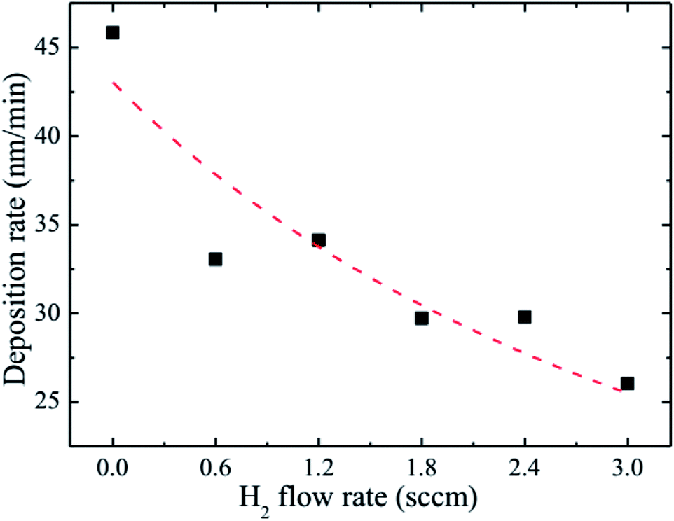 | ||
| Fig. 1 The deposition rate of the HNZO films as a function of the flow rate of H2. | ||
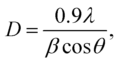
As inferred from the XRD patterns given in Fig. 2 as a function of the flow rate of H2, all the HNZO films exhibited a (002) diffraction peak around 34°—which is an indication of a typical wurtzite structure whose c-axis was preferentially perpendicular to the substrate. The XRD patterns does not show any indication of the presence of any phase which corresponds to the dopants, which is either a reflection of the substitution of the incorporated Nb ions for Zn ions in the hexagonal lattice or an indication of the segregation of the Nb ions into non-crystalline regions at the grain boundaries. The XRD pattern of the NZO film (0 sccm of H2) shows other peaks such as (101), (102), (103) and (200) besides the dominant (002) and (004) peaks (Fig. 2(b)). These structural observations are consistent with self-textured ZnO films prepared by low-pressure chemical vapor deposition method43 or ultrasonic spray pyrolysis method.44 The other abovementioned diffraction peaks can be attributed to the creation of a pyramid-like surface morphology (see Fig. 2(b)). The intensity of the (002) reflection was found to initially decrease upon the introduction of H2, and to subsequently increase when the flow rate of H2 was increased to 1.2 sccm; however, for H2 flow rates beyond this value, the (002) orientation was less favored. This observation can be explained by taking the high-energy O2− ion bombardment of the NZO film into account; that is, the ion bombardment damages the (002) planes more seriously than other loosely-packed planes such as (101)—the surface of the growing film will have a large number of dangling bonds;45,46 therefore, the growth of the crystallites that are normal to the (101) plane will continue relatively undisturbed, and they can serve as seeds for further growth;45,46 however, the termination of the dangling bonds upon the incorporation of hydrogen enables the sputtered atoms to travel further. Upon the hydrogen doping, the microstructure of the NZO film changes from an unstable to a more stable orientation, i.e. (101) or (200) to (002) plane growth—thanks to the lowest surface energy of the (002) crystal plane.47 H2 flow rates more than 1.2 sccm can considerably reduce the (002) peak intensity; that is, the H dopant concentration in excess of the saturation stage deteriorates the crystal quality of the NZO films, and arrests the (101) and (200) plane growth.48 Fig. 3 presents the full-width-at-half-maximum (FWHM) of the (002) peak, and the grain size (D) calculated according to Scherrer formula49
 | (1) |
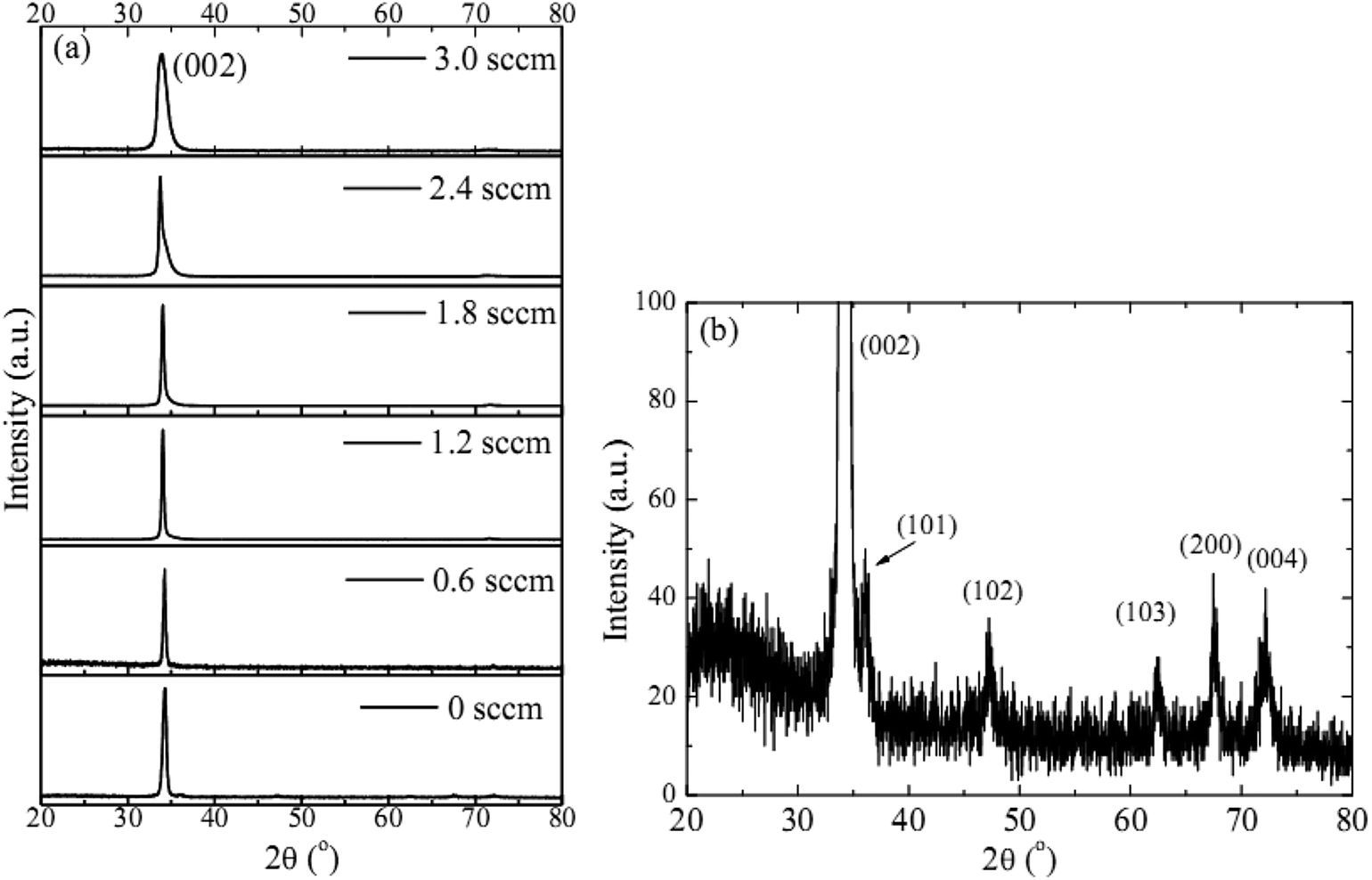 | ||
| Fig. 2 (a) The XRD patterns of the HNZO films as a function of the flow rate of H2, (b) the amplified XRD pattern of the NZO film (0 sccm of H2). | ||
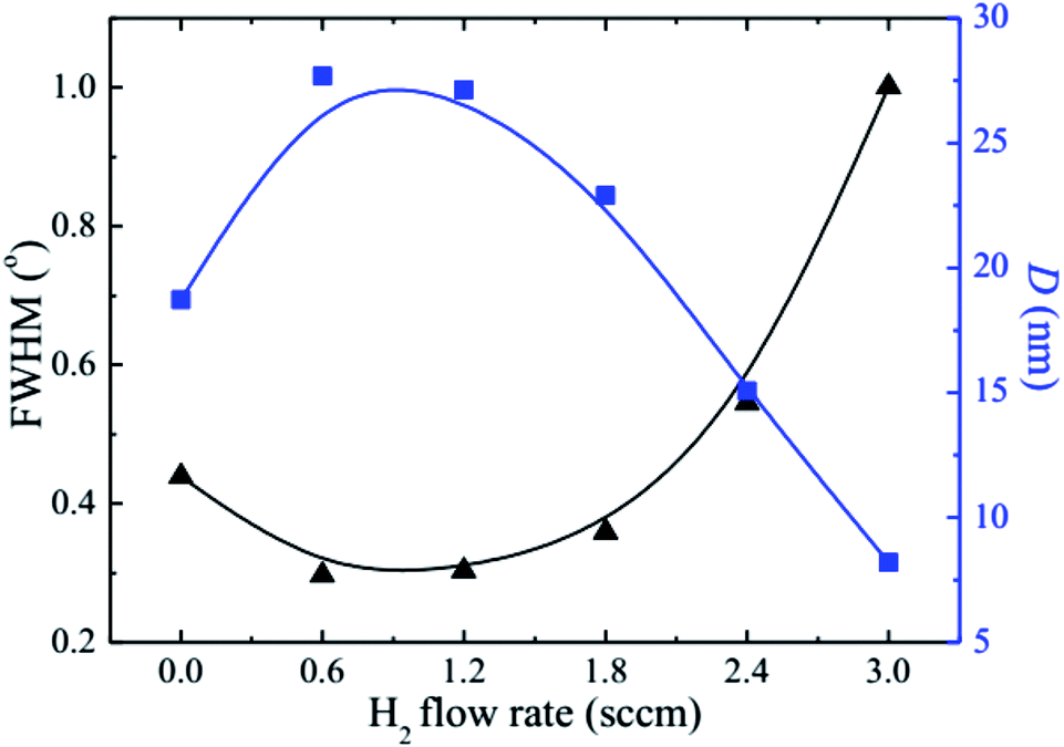 | ||
| Fig. 3 The FWHM and crystallite size (D) of the HNZO films as a function of the flow rate of H2. | ||
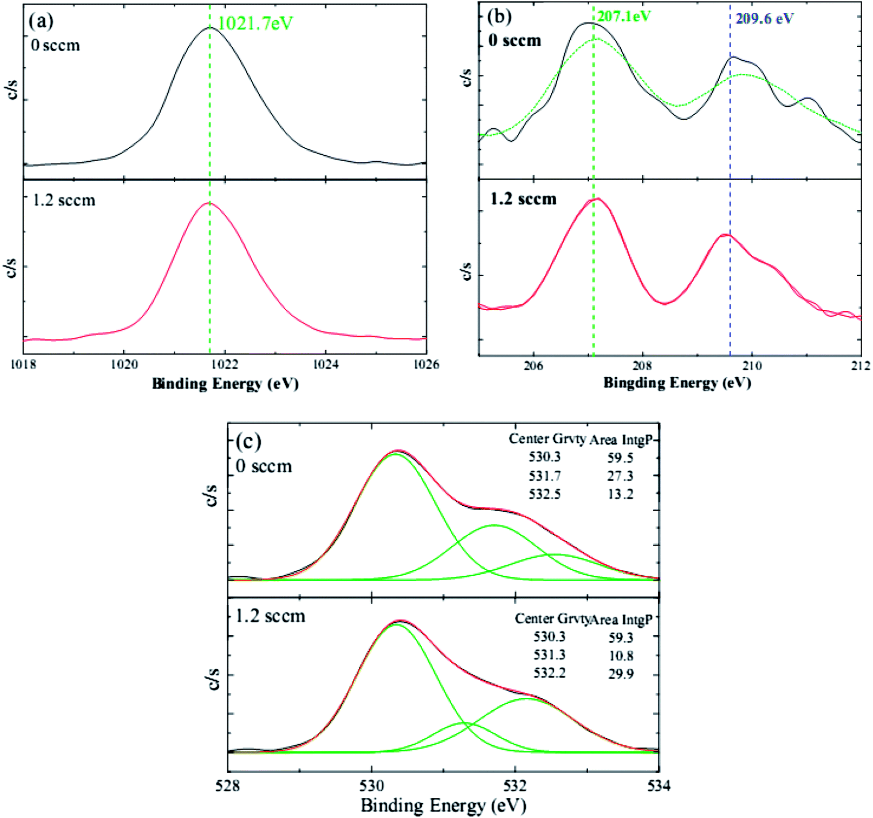
To better understand the doping mechanism of H into the NZO films, the valence states Zn, Nb, and O of one NZO film and one HNZO film that was fabricated at the hydrogen flow rate of 1.2 sccm were inspected using XPS measurements. Fig. 4 shows the typical XPS spectra of Zn, Nb, and O. The symmetry of the core lines of Zn 2p3/2 located at 1021.7 ± 0.1 eV (ref. 50 and 51) suggest that Zn atoms mainly remain in the same formal valence state of Zn2+ in both the NZO and HNZO films—the incorporated H does not influence the combined state of Zn. Consistent with the aforementioned XRD analysis, the XPS spectrum does not show any indication of the presence of metallic Zn peak, which reflects that the Zn exists only in the oxidized state. Moreover, the two peaks of Nb 3d5/2 and 3d3/2 at respectively 207.1 ± 0.1 eV (ref. 52) and 209.6 ± 0.2 eV (ref. 53) indicate that the Nb is in its oxidation state (Nb5+), takes the place of the Zn2+ in the NZO film in the form of an Nb–O bond, and becomes a substitute for the Zn2+ in the HNZO film as an Nb–O or Nb–H–O bond.54 Three O peaks are observed in the XPS spectrum for both the NZO and HNZO films (Fig. 4(c)). The low-energy component of the NZO film at 530.4 ± 0.1 eV is attributed to the oxygen ions surrounded by the Zn (or by substitutional Nb) atoms,55 whereas the peak at the higher binding energy of 531.7 ± 0.4 eV is due to the oxygen ions within those regions of the ZnO matrix that are deficient of oxygen.56,57 The peak with the highest binding energy that is located at 532.4 ± 0.2 eV corresponds to chemisorbed or dissociated oxygen or hydroxyl species such as adsorbed O2.58 Fig. 4(c) shows that the incorporation of hydrogen makes the integral area of the middle-binding-energy peak decrease from 27.3% to 10.8%, and the integral area of the peak with the highest binding energy increase from 13.2% to 29.9%. Such change is put down to the formation of O–H bonding as Van de Walle predicted by first-principle calculations.27,58
 | ||
| Fig. 4 The typical XPS spectra of (a) Zn 2p, (b) Nb 3d, and (c) O 1s of the NZO films with and without H doping. | ||
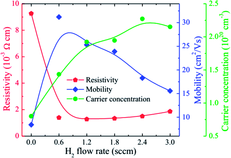
Fig. 5 gives the carrier concentration (n), mobility (μ), and resistivity (ρ) of the HNZO films as a function of the flow rate of H2. The resistivity of the unhydrogenated NZO film (9.26 × 10⁻³ Ω cm) is lower than that of the pure ZnO film, which is mainly attributed to the substitutional effect of Nb5+ ions on the remaining Zn2+ ions (Fig. 4(b)). Upon the incorporation of H, the resistivity of the NZO film is markedly lowered than that of the pure NZO film. When the hydrogen flow rate was increased, the resistivity was first decreased, and was then maximized when the hydrogen flow rate reached 1.2 sccm; this is attributed to the increase in both n and μ, thanks to a small amount of hydrogen doping. Further increase of the flow rate of H2 to 2.4 sccm led to n reaching a maximum, and to μ decreasing monotonically. The formation energy of the O–H stretch (in the H+ form) in the Zn–O is the lowest, and the doped hydrogen in ZnO films is an n-type donor.27,59 Furthermore, hydrogen can be interstitially incorporated into ZnO-related films, and can form dangling bonds in grain boundaries.60 The increase in n upon the incorporation of hydrogen is attributed to the formation of the O–H stretch in Zn–O bonds. The decrease in μ with increasing the flow rate of H2 may be put down to ionized impurity scattering and grain boundary scattering that could be because of more hydrogen atoms and smaller grain size in the films (Fig. 3). We found that the optimal value of the H2 flow rate is 1.2 sccm with ρ being 1.28 × 10⁻³ Ω cm, n being 1.92 × 1020 cm−3, and μ being 25.32 cm2 V−1 s−1. The beneficial effect of hydrogen doping was also observed in fluorine-doped ZnO films.42
 | ||
| Fig. 5 The carrier concentration (n), mobility (μ), and resistivity (ρ) of the HNZO films as functions of the flow rate of H2. | ||
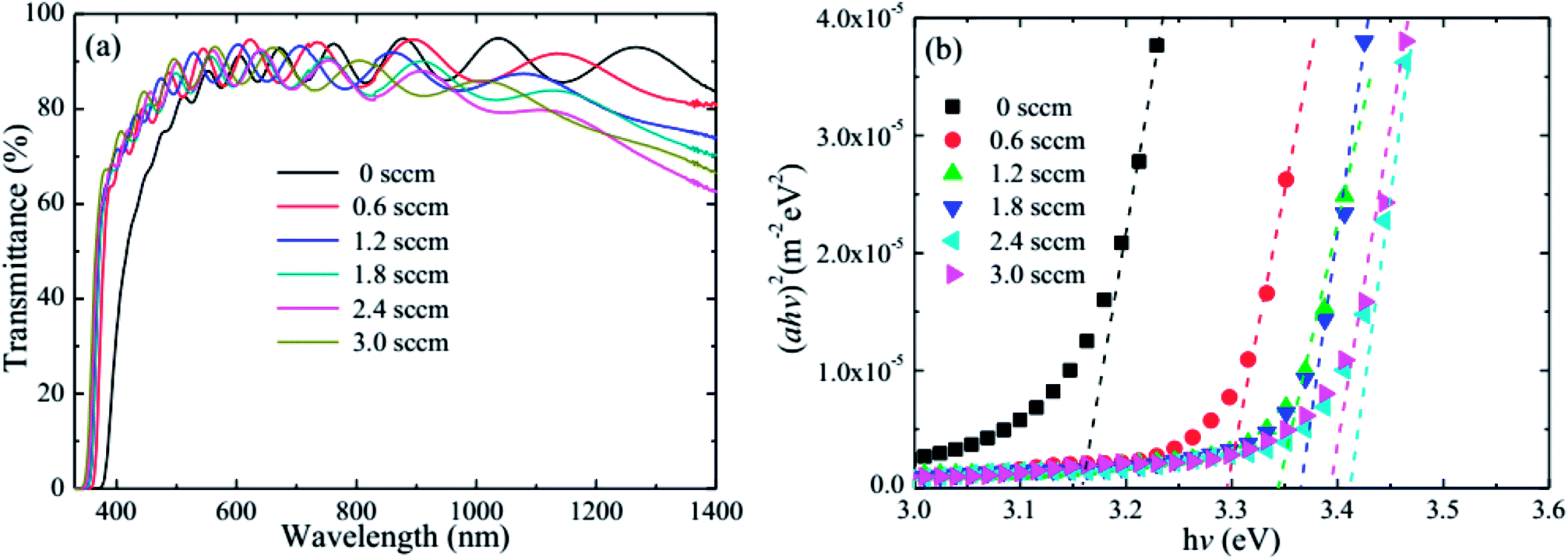
Fig. 6 shows the optical transmittance and optical band gap of the HNZO films as a function of the H2 flow rate. The optical transmittance strongly depends on the flow rate. When flow rate increases, the absorption edge of the film shifts to the short wavelength region, being an indication of the broadening of the optical band gap of the HNZO films; the transmittance is also significantly improved around 400 nm. This is understood by the Burstein–Moss effect—the upward shift of the Fermi level inside the conduction band because of an increased donor concentration which leads to the conduction band being further filled by an increased number of electron carriers.61 Although the hydrogen-induced increase of carrier concentration reduces the long-wavelength transmittance, the transmittance of the HNZO films in the range of 400–1400 nm is on average about 85%.
 | ||
| Fig. 6 (a) The optical transmittance, and (b) optical band gap of the HNZO films as a function of the flow rate of H2. | ||
The optical band gap (Eg) as a function of the flow rate is determined by applying the Tauc model in the high-absorbance region62
| αhv = D(hv − Eg)n, | (2) |
In order that the special requirements of thin-film solar cells for front contact are met, the TCO films should also enjoy high chemical stability besides they exhibit good optical and electrical properties. We tested the chemical stability of the abovementioned electrically- and optically-optimal HNZO films by etching them in diluted HCl and NaOH for different time periods. For comparison, the sputtered AZO films were also etched using the same experimental procedures.
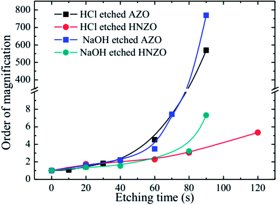
Fig. 7 shows multiple changes of sheet resistance for the etched AZO and HNZO films. The sheet resistances of the as-deposited AZO and HNZO films were 7.8 Ω □−1 and 13.5 Ω □−1, respectively. As shown in Fig. 7, almost no changes were observed in both the AZO and HNZO samples etched for less than 40 seconds in either HCl or NaOH solutions. However, when the samples were etched for more than 40 seconds, the order of magnification was sharply increased for both the HCl- and NaOH-etched AZO films. On the contrary, the corresponding changes for both of the HCl- and NaOH-etched HNZO films are relatively small. When the etching time of the HCl-etched HNZO film was increased from 60 s to 120 s, its order of magnification was increased only from 2.3 to 5.3; this change of order of magnification for the NaOH-etched HNZO film was from 3.2 to 7.3 when the etching time was increased from 80 s to 90 s. Therefore, the HNZO films are highly chemically-stable, which demonstrates their potential for broad applications in thin-film solar cells.
 | ||
| Fig. 7 The multiple changes of the sheet resistance of the HCl- and NaOH-etched AZO and HNZO films at different etching times. | ||
4. Conclusion
In this study, transparent conducting HNZO films were deposited using the RFMS method on glass substrates. The structural, electrical, and optical properties of the NZO films were investigated as a function of the H2 flow rate. All of the as-deposited films possessed good crystallinity with a c-axis preferential orientation, low room-temperature resistivity, and high broadband spectrum transmittance of more than 85% at the range of 400 to 1400 nm. The lowest resistivity of 1.28 × 10⁻³ Ω cm, with a Hall mobility of 25.32 cm2 V−1 s−1, and an electron concentration of 1.92 × 1020 cm−3 were achieved at the H2 flow rate of 1.2 sccm. Furthermore, the carrier concentration was mainly originated from the substitution of Nb5+ for Zn2+, and from the formation of Zn–H–O and Nb–H–O bonds. The HNZO films have high acid and alkali resistance, which demonstrates their potential for broad applications in optoelectronic devices.Conflicts of interest
There are no conflicts to declare.Acknowledgements
The work was supported by the National Natural Science Foundation of China (Grant No. 11404088), the Third Batch of Young Top-notch Talent Fund of Hebei Province (China), Natural Science Foundation of Hebei Province (Grant No. F2015405011), Talent Training Funding for Scientific Research Project of Hebei Province (Grant No. A2016002020), General Projects of Hebei North University (Grant No. YB2018014), Major Projects of Hebei North University (Grant No. ZD201401), and the Doctoral Scientific Research Foundation of Hebei North University.References
- D. S. Ginley, C. Bright and G. Li, Transparent conducting oxides, MRS Bull., 2000,(25), 15–18 CrossRef CAS.
- C. G. Granqvist, Transparent conductors as solar energy materials: a panoramic review, Sol. Energy Mater. Sol. Cells, 2007, 91, 1529–1598 CrossRef CAS.
- W. T. Yen, Y. C. Lin and J. H. Ke, Surface textured ZnO: Al thin films by pulsed DC magnetron sputtering for thin film solar cells applications, Appl. Surf. Sci., 2010, 257, 960–968 CrossRef CAS.
- E. Moulin, K. Bittkau, M. Ghosh, G. Bugnon, M. Stuckelberger, M. Meier, F. J. Haug, J. Hüpkes and C. Ballif, Comparison of LPCVD and sputter-etched ZnO layers applied as front electrodes in tandem thin-film silicon solar cells, Sol. Energy Mater. Sol. Cells, 2016, 145, 185–192 CrossRef CAS.
- J. Nomoto, M. Konagai, K. Okada, T. Ito, T. Miyata and T. Minami, Comparative study of resistivity characteristics between transparent conducting AZO and GZO thin films for use at high temperatures, Thin Solid Films, 2010, 518, 2937–2940 CrossRef CAS.
- L. V. Mercaldo, I. Usatii, E. M. Esposito, P. D. Veneri, J. W. Schüttauf, E. Moulin, F. J. Haug, C. Zhang and M. Meier, Metal versus dielectric back reflector for thin-film Si solar cells with impact of front electrode surface texture, Prog. Photovolt: Res. Appl., 2016, 24, 968–977 CrossRef CAS.
- K. C. Lai, J. H. Wang, C. Lu, F. J. Tsai, C. H. Yeh and M. P. Houng, Plasma-induced TCO texture of ZnO:Ga back contacts on silicon thin film solar cells, Sol. Energy Mater. Sol. Cells, 2011, 95, 415–418 CrossRef CAS.
- K. H. Ri, Y. Wang, W. L. Zhou, J. X. Gao, X. J. Wang and J. Yu, The structural properties of Al doped ZnO films depending on the thickness and their effect on the electrical properties, Appl. Surf. Sci., 2011, 258, 1283–1289 CrossRef CAS.
- C. Agashe, O. Kluth, G. Schope, H. Siekmann, J. Hüpkes and B. Rech, Optimization of the electrical properties of magnetron sputtered aluminum-doped zinc oxide films for opto-electronic applications, Thin Solid Films, 2003, 442, 167–172 CrossRef CAS.
- J. Yoo, J. Lee, S. Kim, K. Yoon, I. J. Park, S. K. Dhungel, B. Karunagaran, D. Mangalaraj and J. Yi, High transmittance and low resistive ZnO:Al films for thin film solar cells, Thin Solid Films, 2005, 480–481, 213–217 CrossRef CAS.
- S. M. Jung, Y. H. Kim, S. I. Kim and S. I. Yoo, Characteristics of transparent conducting Al-doped ZnO films prepared by dc magnetron sputtering, Curr. Appl. Phys., 2011, 11, S191–S196 CrossRef.
- T. J. Coutts, D. L. Young and X. N. Li, Characterization of Transparent Conducting Oxides, MRS Bull., 2000, 58–65 CrossRef CAS.
- S. Parthiban, E. Elangovan, K. Ramamurthi, R. Martins and E. Fortunato, Investigations on high visible to near infrared transparent and high mobility Mo doped In2O3 thin films prepared by spray pyrolysis technique, Sol. Energy Mater. Sol. Cells, 2010, 94, 406–412 CrossRef CAS.
- M. Y. Wu, S. H. Yu, L. He, G. Zhang, D. X. Ling and W. F. Zhang, Influence of oxygen pressure on the structural, electrical and optical properties of Nb-doped ZnO thin films prepared by pulsed laser deposition, Appl. Surf. Sci., 2014, 292, 219–224 CrossRef CAS.
- K. Bergum, P. A. Hansen, H. Fjellvåg and O. Nilsen, Structural, electrical and optical characterization of Ti-doped ZnO films grown by atomic layer deposition, J. Alloys Compd., 2014, 616, 618–624 CrossRef CAS.
- O. Angelov, K. Lovchinov and D. D. Malinovska, Optical and electrical properties of ZnO thin films doped with Al, V and Nb, Phys. Status Solidi C, 2013, 10, 709–712 CrossRef CAS.
- F. H. Wang and C. L. Chang, Effect of substrate temperature on transparent conducting Al and Fnco-doped ZnO thin films prepared by rf magnetron sputtering, Appl. Surf. Sci., 2016, 370, 83–91 CrossRef CAS.
- X. L. Chen, J. M. Liu, J. Ni, Y. Zhao and X. D. Zhang, Wide-spectrum Mg and Ga co-doped ZnO TCO thin films for solar cells grown via magnetron sputtering with H2 introduction, Appl. Surf. Sci., 2015, 328, 193–197 CrossRef CAS.
- I. Y. Kim, S. W. Shin, M. G. Gang, S. H. Lee, K. V. Gurav, P. S. Patil, J. H. Yun, J. Y. Lee and J. H. Kim, Comparative study of quaternary Mg and group III element co-doped ZnO thin films with transparent conductive characteristics, Thin Solid Films, 2014, 570, 321–325 CrossRef CAS.
- S. W. Shin, G. L. Agawane, I. Y. Kim, S. H. Jo, M. S. Kim, G. S. Heo, J. H. Kim and J. Y. Lee, Development of transparent conductive Mg and Ga co-doped ZnO thin films: Effect of Mg concentration, Surf. Coat. Technol., 2013, 231, 364–369 CrossRef CAS.
- J. Liu, W. Zhang, D. Song, Q. Ma, L. Zhang, H. Zhang, X. Ma and H. Song, Comparative study of the sintering process and thin film sputtering of AZO, GZO and AGZO ceramics targets, Ceram. Int., 2014, 40, 12905–12915 CrossRef CAS.
- S. U. Park and J. H. Koh, Low temperature rf-sputtered In and Al co-doped ZnO thin films deposited on flexible PET substrate, Ceram. Int., 2014, 40, 10021–10025 CrossRef CAS.
- C. A. Gupta, S. Mangal and U. P. Singh, Impact of rapid thermal annealing on structural, optical and electrical properties of DC sputtered doped and co-doped ZnO thin film, Appl. Surf. Sci., 2014, 288, 411–415 CrossRef CAS.
- G. X. Liu, F. K. Shan, W. J. Lee, B. C. Shin, H. S. Kim and J. H. Kim, Boron and nitrogen co-doped ZnO thin films for opto-electronic applications, Ceram. Int., 2008, 34, 1011–1015 CrossRef CAS.
- F. Zhu-Ge, Z. Z. Ye, L. P. Zhu, J. G. Lü, B. H. Zhao, J. Y. Huang, Z. H. Zhang, L. Wang and Z. G. Ji, Electrical and optical properties of Al–N co-doped p-type zinc oxide films, J. Cryst. Growth, 2004, 268, 163–168 CrossRef.
- K. Shtereva, S. Flickyngerova, V. Tvarozek, I. Novotny, J. Kovac and A. Vincze, Characterization of gallium–nitrogen co-doped zinc oxide thin films prepared by RF diode sputtering, Vacuum, 2012, 86, 652–656 CrossRef CAS.
- C. G. Van de Walle, Hydrogen as a cause of doping in zinc oxide, Phys. Rev. Lett., 2000, 85, 1012–1015 CrossRef CAS PubMed.
- C. G. Van de Walle, Defect analysis and engineering in ZnO, Physica B Condens. Matter, 2001, 308–310, 899–903 CrossRef CAS.
- C. G. Van de Walle and J. Neugebauer, Universal alignment of hydrogen levels in semiconductors, insulators and solutions, Nature, 2003, 423, 626–628 CrossRef CAS PubMed.
- B. Y. Oh, M. C. Jeong, D. S. Kim, W. Lee and J. M. Myoung, Post-annealing of Al-doped ZnO films in hydrogen atmosphere, J. Cryst. Growth, 2005, 281, 475–480 CrossRef CAS.
- B. Y. Oh, M. C. Jeong and J. M. Myoung, Stabilization in electrical characteristics of hydrogen-annealed ZnO: Al films, Appl. Surf. Sci., 2007, 253, 7157–7161 CrossRef CAS.
- S. J. Baik, J. H. Jang, C. H. Lee, W. Y. Cho and K. S. Lim, Highly textured and conductive undoped ZnO film using hydrogen posttreatment, Appl. Phys. Lett., 1997, 70, 3516–3518 CrossRef CAS.
- S. Y. Myong and K. S. Lim, Highly stable and textured hydrogenated ZnO thin films, Appl. Phys. Lett., 2003, 82, 3026–3028 CrossRef CAS.
- M. S. Myong, S. I. Park and K. S. Lim, Improvement of electrical stability of polycrystalline ZnO thin films via intentional post-deposition hydrogen doping, Thin Solid Films, 2006, 513, 148–151 CrossRef.
- Y. S. Kang, H. Y. Kim and J. Y. Lee, Effects of Hydrogen on the Structural and Electro-optical Properties of Zinc Oxide Thin Films, J. Electrochem. Soc., 2000, 147, 4625–4629 CrossRef CAS.
- L. Y. Chen, W. H. Chen, J. J. Wang, F. C. N. Hong and Y. K. Su, Hydrogen-doped high conductivity ZnO films deposited by radio-frequency magnetron sputtering, Appl. Phys. Lett., 2004, 85, 5628–5630 CrossRef CAS.
- M. L. Addonizio, A. Aantonaia, G. Cantele and C. Privato, Transport mechanisms of RF sputtered Al-doped ZnO films by H2 process gas dilution, Thin Solid Films, 1999, 349, 93–99 CrossRef CAS.
- Y. M. Chung, C. S. Moon, W. S. Jung and J. G. Han, The low temperature synthesis of Al doped ZnO films on glass and polymer using pulsed co-magnetron sputtering: H2 effect, Thin Solid Films, 2006, 515, 567–570 CrossRef CAS.
- T. Yamada, T. Nebiki, S. Kishimoto, H. Makino, K. Awai, T. Narusawa and T. Yamamoto, Dependences of structural and electrical properties on thickness of polycrystalline Ga-doped ZnO thin films prepared by reactive plasma deposition, Superlattices Microstruct., 2007, 42, 68–73 CrossRef CAS.
- S. H. Lee, T. S. Lee, K. S. Lee, B. Cheong, Y. D. Kim and W. M. Kim, Effect of heat treatment of sputter deposited ZnO films co-doped with H and Al, J. Electroceram., 2009, 23, 468–473 CrossRef CAS.
- Y. F. Wang, X. D. Zhang, L. S. Bai, Q. Huang, C. C. Wei and Y. Zhao, Effective light trapping in thin film silicon solar cells from textured Al doped ZnO substrates with broad surface feature distributions, Appl. Phys. Lett., 2012, 100, 263508-1–263508-4 Search PubMed.
- F. H. Wang and T. H. Yang, Effect of hydrogen doping on the properties of Al and F co-doped ZnO films for thin film silicon solar cell applications, Thin Solid Films, 2016, 605, 64–72 CrossRef CAS.
- S. Fäy, L. Feitknecht, R. Schluchter, U. Kroll, E. Vallat-Sauvain and A. Shah, Rough ZnO layers by LP-CVD process and their effect in improving performances of amorphous and microcrystalline silicon solar cells, Sol. Energy Mater. Sol. Cells, 2006, 90, 2960–2967 CrossRef.
- B. C. Jiao, X. D. Zhang, C. C. Wei, J. Sun, Q. Huang and Y. Zhao, Effect of acetic acid on ZnO:In transparent conductive oxide prepared by ultrasonic spray pyrolysis, Thin Solid Films, 2011, 520, 1323–1329 CrossRef CAS.
- J. H. Park, B. K. Shin, H. M. Moon, M. J. Lee, K. I. Park, K. J. Ahn, W. Lee and J. M. Myoung, Effect of the substrate temperature on the properties of Ga-doped ZnO films for photovoltaic cell applications deposited by a pulsed DC magnetron sputtering with a rotating cylindrical target, Vacuum, 2012, 86, 1423–1427 CrossRef CAS.
- T. Serikawa and S. Shirai, Deposition characteristics and properties of SiO2 films prepared by reactive sputtering in hydrogen-, oxygen- and nitrogen-argon mixtures, Jpn. J. Appl. Phys., Part 1, 1994,(33), 7B Search PubMed.
- Y. F. Wang, X. D. Zhang, Q. Huang, F. Yang, J. H. Liang, D. K. Zhang and Y. Zhao, Tailoring of textured ZnO:Al film via hydrogen, Vacuum, 2014, 107, 6–9 CrossRef CAS.
- W. F. Liu, G. T. Du, Y. F. Sun, Y. B. Xu, T. P. Yang, X. S. Wang, Y. C. Chang and F. B. Qiu, Al-doped, ZnO thin films deposited by reactive frequency magnetron sputtering: H2-induced property changes, Thin Solid Films, 2007, 515, 3057–3060 CrossRef CAS.
- Y. F. Wang, Q. Huang, C. C. Wei, D. K. Zhang, Y. Zhao and X. D. Zhang, Improvement of electrical and optical properties of molybdenum doped zinc oxide films by introducing hydrogen, Appl. Surf. Sci., 2012, 258, 8797–8801 CrossRef CAS.
- C. Battistoni, J. L. Dormann, D. Fiorani, E. Paparazzo and S. Viticoli, An XPS and Mössbauer study of the electronic properties of ZnCrxGa2−xO4 spinel solid solutions, Solid State Commun., 1981, 39, 581–586 CrossRef CAS.
- G. Schön, Auger and direct electron spectra in X-ray photoelectron studies of zinc, zinc oxide, gallium and gallium oxide, J. Electron Spectrosc. Relat. Phenom., 1973, 2, 75–86 CrossRef.
- N. Özer, D. G. Chen and C. M. Lampert, Preparation and properties of spin-coated Nb2O5 films by the sol-gel process for electrochromic applications, Thin Solid Films, 1996, 277, 162–168 CrossRef.
- N. Özer, M. D. Rubin and C. M. Lampert, Optical and electrochemical characteristics of niobium oxide films prepared by sol-gel process and magnetron sputtering A comparison, Sol. Energy Mater. Sol. Cells, 1996, 40, 285–296 CrossRef.
- M. A. B. Gomes, L. O. S. Bulhões, S. C. Castro and A. J. Damião, The Electrochromic Process at Nb2O5 Electrodes Prepared by Thermal Oxidation of Niobium, J. Electrochem. Soc., 1990, 137, 3067–3070 CrossRef CAS.
- C. D. Wagner, D. A. Zatko and R. H. Raymond, Use of the oxygen KLL Auger lines in identification of surface chemical states by electron spectroscopy for chemical analysis, Anal. Chem., 1980, 52, 1445–1451 CrossRef CAS.
- T. Szörényi, L. D. Laude, I. Bertóti, Z. Kántor and Zs. Geretovszky, Excimer laser processing of indium-tin-oxide films: An optical investigation, J. Appl. Phys., 1995, 78, 6211–6219 CrossRef.
- J. C. C. Fan and J. B. Good enough, X-ray photoemission spectroscopy studies of Sn-doped indium-oxide films, J. Appl. Phys., 1977, 48, 3524–3531 CrossRef CAS.
- F. H. Wang, H. P. Chang, C. C. Tseng and C. C. Huang, Effects of H2 plasma treatment on properties of ZnO:Al thin films prepared by RF magnetron sputtering, Surf. Coat. Technol., 2011, 205, 5269–5277 CrossRef CAS.
- Y. F. Wang, J. M. Song, W. Zheng, H. L. Pei, X. H. Wang, D. Wang, G. Z. Niu, Q. G. Song, F. Yang and J. Y. Nan, Experimental and theoretical analysis of H and Ti co-doped ZnO transparent conductive films, Ceram. Int., 2017, 43, 5396–5402 CrossRef CAS.
- S. J. Tark, Y. W. Ok, M. G. Kang, H. J. Lim, W. M. Kim and D. Kim, Effect of a hydrogen ratio in electrical and optical properties of hydrogenated Al-doped ZnO films, J. Electroceram., 2009, 23, 548–553 CrossRef CAS.
- G. Li, X. B. Zhu, H. C. Lei, W. H. Song, Z. R. Yang, J. M. Dai, Y. P. Sun, X. Pan and S. Y. Dai, Study on chemical solution deposition of aluminum-doped zinc oxide films, J. Alloys Compd., 2010, 505, 434–442 CrossRef CAS.
- S. Mandal, R. K. Singha, A. Dhar and S. K. Ray, Mater. Res. Bull., 2008, 43, 244–250 CrossRef CAS.
- B. F. Liu, L. S. Bai, T. T. Li, C. C. Wei, B. Z. Li, Q. Huang, D. K. Zhang, G. C. Wang, Y. Zhao and X. D. Zhang, High efficiency and high open-circuit voltage quadruple-junction silicon thin film solar cells for future electronic applications, Energy Environ. Sci., 2017, 10, 1134–1141 RSC.
Footnote |
| † Electronic supplementary information (ESI) available. See DOI: 10.1039/c9ra01231a |
| This journal is © The Royal Society of Chemistry 2019 |