
 Open Access Article
 This Open Access Article is licensed under a Creative Commons Attribution-Non Commercial 3.0 Unported Licence
The magnetism of 1T-MX2 (M = Zr, Hf; X = S, Se) monolayers by hole doping†
Hui Xiang *abc,
Bo Xud,
Weiqian Zhaoa,
Yidong Xiab,
Jiang Yinb,
Xiaofei Zhanga and
Zhiguo Liu*b
*abc,
Bo Xud,
Weiqian Zhaoa,
Yidong Xiab,
Jiang Yinb,
Xiaofei Zhanga and
Zhiguo Liu*b
aSchool of Mathematics and Physics, Hubei Polytechnic University, Huangshi, 435003, China. E-mail: hxiang0717@163.com
bNational Laboratory of Solid State Microstructures, Department of Materials Science and Engineering, Nanjing University, Nanjing, 210093, China. E-mail: liuzg@nju.edu.cn
cSchool of Chemistry and Chemical Engineering, Wuhan University of Science and Technology, Wuhan, 430081, China
dSchool of Sciences, Key Laboratory of Biomedical Functional Materials, China Pharmaceutical University, Nanjing, 211198, China
First published on 2nd May 2019
Abstract
The magnetism of hole doped 1T-MX2 (M = Zr, Hf; X = S, Se) monolayers is systematically studied by using first principles density functional calculations. The pristine 1T-MX2 monolayers are semiconductors with nonmagnetic ground states, which can be transformed to ferromagnetic states by the approach of hole doping. For the unstrained monolayers, the spontaneous magnetization appears once above the critical hole density (1014 cm−2), where the p orbital of S or Se atoms contributes the most of the magnetic moment. As the tensile strains exceed 4%, the magnetic moments per hole of ZrS2 and HfS2 monolayers increase sharply to a saturated value with increasing hole density, implying obvious advantages over the unstrained monolayers. The phonon dispersion calculations for the strained ZrS2 and HfS2 monolayers indicate that they can keep the dynamical stability by hole doping. Furthermore, we propose that the fluorine atom modified ZrS2 monolayer could obtain stable ferromagnetism. The magnetism in hole doped 1T-MX2 (M = Zr, Hf; X = S, Se) monolayers has great potential for developing spintronic devices with desirable applications.
1 Introduction
Since atomically thick transition metal dichalcogenides (TMDCs) can be synthesized in experiments, they have been considered as promising candidates for next generation nanoelectronics, due to their interesting physical phenomena, including the quantum spin Hall effect, valley polarization, two-dimensional superconductivity, and so on.1–8 Zirconium and hafnium dichalcogenides MX2 (M = Zr, Hf; X = S, Se), one group of TMDCs, have attracted attention due to their unique electrical and optoelectronic properties.9–13 ZrS2 nanobelt photodetectors have demonstrated excellent electrical transport and high-performance photoconductivity, such as a response time of ∼2 μs, responsivity of 7.1 × 10⁵ A W−1, and a quantum efficiency of 1.8 × 10⁸%.10 The acoustic phonon limited room-temperature electron mobility of MX2 (M = Zr, Hf; X= S, Se) monolayers can be above 1200 cm2 V−1 s−1, which is much higher than that of MoS2 (340 cm2 V−1 s−1), SnS2 (306 cm2 V−1 s−1) and some other TMDCs.11 As we know, spintronic devices play an important role in promising applications in information storage and processing. Significantly, previous studies have found that the magnetism based on the sp states of nonmetal elements has some obvious advantages, such as stronger long-range exchange coupling interactions and no clustering of magnetic ions, which generally enhance the electronic spin transport and spin-polarization.14,15 The efficient electron transport characteristic in MX2 (M = Zr, Hf; X = S, Se) monolayers would be important in spin electronics. Unfortunately, most two dimensional (2D) TMDCs, including MX2 (M = Zr, Hf; X = S, Se), are naturally nonmagnetic, which largely limits their applications.It is generally that the magnetic and spin polarization strongly depends on the electronic structures near the Fermi level (EF). Once the density of states (DOS) near the Fermi level is large enough to satisfy the “Stoner criterion”,16 the spin splitting would occur. In past years, the electronic structures can be tunable by using several methods. Of particular concern is that the strain engineering is commonly used to tune the electronic structures in 2D TMDCs, which is because of their superior elasticity and structural stability to one atomic thick crystals and bulk in a wide range of strain.17–19 By applying strains, previous studies predicted the switched ferromagnetism in TMDCs monolayers, such as VX2 and NbX2 (X = S, Se), and CrX2 (X = Se, Te). Besides, carrier doping is considered as another effective approach to modulate EF. Cao et al.20 and Huang et al.21 reported the theoretical investigation of magnetism in GaSe and silicon phosphides, respectively. We also systematically studied the strain tunable magnetism of SnX2 (X = S, Se) and graphene-like C2N by hole doping in previous work.22,23 To obtain the carrier doping, there are several approaches availably in experiments, such as electric-field control in field effect transistors (FETs),24–26 introducing impurity atoms or vacancies,27 adatom decoration in 2D nanosheets28,29 and so on.
For MX2 (M = Zr, Hf; X = S, Se) monolayers, previous studies have indicated that electronic structures can be effectively tuned by mechanical strain.30,31 In this work, strain engineering and carrier doping are both employed. We report the realization of the magnetism on hole doped 1T-MX2 (M = Zr, Hf; X = S, Se) monolayers on the basis of first-principle calculations. We find that four monolayers can be magnetized by hole doping. When the strains reach 4%, the magnetic moments of hole doped disulfides can be obviously increased to constants with lower critical hole density in comparison with the unstrained states. Moreover, fluorine doped ZrS2 monolayer is a p-type semiconductor, meaning that the fluorination is one of effective ways to realize hole doping. We also predicted that the fluorinated ZrS2 monolayer shows stable ferromagnetic property. Therefore, ZrS2 and HfS2 monolayers could be considered as viable candidates for spintronic devices.
2 Computational methods
To study the electronic and magnetic properties of the MX2 (M = Zr, Hf; X = S, Se) monolayers, density functional theory (DFT) calculations were performed using the Projector-Augmented Wave (PAW) pseudopotential implementation of the Vienna Ab Initio Simulation Package (VASP).32–34 Electron exchange and correlation effects were described by the generalized gradient approximation (GGA) functional of Perdew–Burke–Ernzerhof (PBE) formula.35 The energy cutoff for the plane-wave basis was set as 550 eV on the 11 × 11 × 1 Monkhorst–Pack k-point grid for all simulations. The convergence threshold was 1 × 10⁻⁵ eV for the electronic self-consistent field iterations. The atomic positions were optimized until the maximum Hellman–Feynman force on each atom was less than 10−2 eV Å−1. A vacuum spacing of 20 Å was placed to avoid the interactions between the monolayers and its periodic images. Moreover, to examine the dynamical stability of strained MX2 monolayers by hole doping, the phonon dispersions were calculated by density functional perturbation theory (DFPT) in VASP & phonopy.3 Results and discussion
3.1 Geometric structures
The hexagonal crystal structures of 1T-MX2 (M = Zr, Hf; X= S, Se) monolayers with a globally D3d point-group symmetry are covalently bonded by octahedrally-coordinated sandwich layers, where the central M atom in the octahedron bonds to six nearest-neighbor X atoms located in the top and bottom sublayers, as shown in Fig. 1. Each primitive hexagonal unit cell, marked by the rhombus with red dashed line, contains one transition metal and two chalcogenide atoms. Before investigating the strain effect on magnetic properties of MX2 monolayers, we first relaxed the lattice constants and atomic positions to obtain the optimized geometric structures. The optimized geometric parameters of MX2 monolayers are listed in Table 1, which are excellently consistent with the values previously reported,31,36 and slightly larger than that of bulk TMDCs.37 Besides, we also studied the mechanical properties of MX2 monolayers. The elastic stiffness constants C11 (along the x direction) and Poisson ratio ν are listed in Table 1. The value of C11 are about 64–80 N m−1, which are much smaller than that of graphene (352 N m−1), BN (290 N m−1), MoS2 (130 N m−1), and MoSe2 (108 N m−1), respectively.38,39 Therefore, 1T-MX2 (M = Zr, Hf; X = S, Se) monolayers perform better flexibility along the in-plane direction. | ||
| Fig. 1 (a) The crystal structures of optimized 1T-MX2 (M = Zr, Hf; X = S, Se) monolayers, where the images above and below represent the top and side view, respectively. The green and yellow balls represent the transition metals and chalcogenide atoms, respectively. The red dotted rhombus represents the unit cell. (b) The band structure and DOS of ZrS2 monolayer. The red and blue lines in the right image represent the contribution of the 3p orbital of S atoms and the 4d orbital of Zr atom, respectively. | ||
| Materials | a0 (Å) | a0 (Å) (exp. bulk) | h (Å) | dM–X (Å) | θX–M–X (°) | C11 (N m−1) | ν | Eg (eV) |
|---|---|---|---|---|---|---|---|---|
| a Ref. 36.b Ref. 37. | ||||||||
| ZrS2 | 3.684 (3.691a) | 3.66b | 2.915 | 2.578 | 88.82 | 75 | 0.20 | 1.16 |
| ZrSe2 | 3.797 (3.806a) | 3.76b | 3.175 | 2.707 | 90.92 | 64 | 0.21 | 0.57 |
| HfS2 | 3.647 (3.646a) | 3.62b | 2.888 | 2.553 | 88.85 | 80 | 0.18 | 1.44 |
| HfSe2 | 3.772 (3.771a) | 3.73b | 3.147 | 2.687 | 90.84 | 69 | 0.19 | 0.74 |
3.2 Electronic structures
Electronic properties of MX2 (M = Zr, Hf; X = S, Se) monolayers are also studied by employing PBE functional. Four compounds of MX2 monolayers are indirect band-gap semiconductors, and the valence band maximum (VBM) and conduction band minimum (CBM) in the Brillouin zone are located at the Γ and M points, respectively. The band gaps Eg listed in Table 1 predicted that the Eg of Zr and Hf disulfides are nearly twice that of corresponding diselenides, respectively. Herein, we take an example of the band structure and DOS of ZrS2, as shown in Fig. 1(b), others are depicted in Fig. S1.† The VBM and CBM are mainly attributed to the 3p orbital of S atoms and the 4d orbital of Zr atoms, respectively. The small dispersion near the Γ point indicates the outstanding electron mobility, which is in accordance with the previous values reported by Zhang et al.11 The electronic structures of three other MX2 monolayers are similar to that of ZrS2.3.3 Magnetism of MX2 monolayers
It is clear that MX2 (X = Zr, Hf; X = S, Se) monolayers have excellent mechanical and electronic properties, such as the superior flexibility and carrier mobility, which indicates their promising applications in electronic and optoelectronic devices. To extend their applications in spintronic devices, we systematically studied the magnetism of MX2 monolayers by using carrier doping.By using hole injection to tune the Fermi level, MX2 (M = Zr, Hf; X = S, Se) monolayers can be modulated to be p-type semiconductors with the relatively large EF, caused by the changes of S_p or Se_p orbitals, and consequently would provide the possibility to develop a spontaneous ferromagnetism. We applied hole doping to investigate the possible ferromagnetism in MX2 monolayers. Fig. 2 shows the local magnetic moment per hole and the spin-polarization energy per hole ΔEp (i.e., the total energy difference between the spin-polarized state and non-spin-polarized state normalized by the number of holes) under the various hole density nh. At the nonmagnetic ground state, both the magnetic moment and ΔEp are nearly zero. Once above the critical hole density nhc, the magnetic moments and the absolute values of ΔEp firstly increase and then gradually return to zero. When the nh are around 2.5 × 1014 cm−2, the maximum values of magnetic moment are about 0.7, 0.26, 0.61 and 0.24 μB per hole for ZrS2, ZrSe2, HfS2 and HfSe2, respectively, which are mainly contributed by the p orbitals of S or Se atoms. The minimum of ΔEp are about −15, −7, −13 and −8 meV per hole for ZrS2, ZrSe2, HfS2 and HfSe2, respectively. Therefore, by using hole doping, both the magnetic moments and ferromagnetic stabilities at ground state indicate that ZrS2 (HfS2) would have superior characteristics in comparison with ZrSe2 (HfSe2).
 | ||
| Fig. 2 Hole density dependence of the magnetic moment per hole (a) and the spin polarization energy per hole (b). | ||
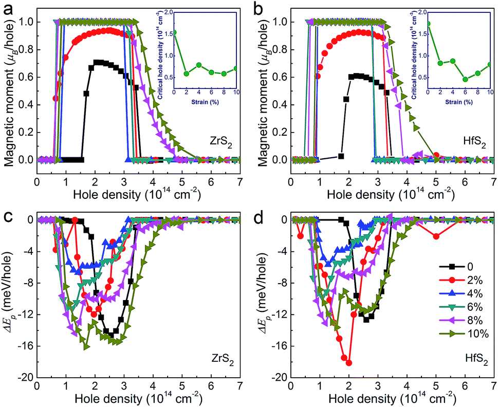
For the unstrained structures, the critical hole densities are about 1.6 × 1014 cm−2 and 1.8 × 1014 cm−2 for ZrS2 and HfS2, respectively. The high hole density would bring unexpected uncontrollability and difficulty for their practical applications. And even worse, the nonzero magnetic moment can be existed in the very narrow range, which would be limited their potential in spintronics. As we known, in most 2D materials, strain engineering is one of effective approaches to modulate the electronic structures, due to their excellent elasticity and structural stability in a wide range of strain. Recently, we reported the effects of biaxial strain on the electronic structures for SnS2 and SnSe2 monolayers.22 It predicted an obvious increment of the DOS near the valence band edges, resulting in the reduction of the critical hole density to ∼1013 cm−2 when the strain reached 4% (6%) in SnS2 (SnSe2). Based on the magnetism of MX2 (M = Zr, Hf; X = S, Se) monolayers displayed above, the biaxial in-plane strains [2%, 10%], with an increment of 2%, were applied to ZrS2 and HfS2. Fig. 3 shows the evolution of the DOS near the valence band edges. It is clear that the DOS near the VBM increases with increasing the strain. While the strain exceeds 4%, the values of EF are close to VBM, and the Mexican-hat-like dispersions are formed around Γ points. Such large EF would lead to a ferromagnetic state with the lower hole density in comparison with the unstrained structure.
 | ||
| Fig. 3 The evolution of DOS near the valence band edges for ZrS2 (a) and HfS2 (b) with the strain from 2% to 10%, where the black lines represent the unstrained structures. | ||
The local magnetic moments of ZrS2 and HfS2 under the biaxial strains in the range of [0%, 10%] are shown in Fig. 4(a) and (b), respectively. Compared with the unstrained structures, the magnetic moment per hole increases with the increment of the strains, more importantly, the critical hole density of the ferromagnetic transition dramatically reduces. When the strains exceed 4%, provided nh < 1.0 × 1014 cm−2, the magnetic moment per hole increases sharply to a saturated value of 1.0 μB per hole with having a plateau region. For example, applying the strain of 6%, the critical hole densities are about 7 × 1013 cm−2 and 5 × 1013 cm−2 for ZrS2 and HfS2, respectively, which are much lower than those of unstrained structures. The saturated magnetic moment per hole can be maintained till the hole density is up to around 3.0 × 1014 cm−2, and then ZrS2 and HfS2 return to nonmagnetic states.
 | ||
| Fig. 4 Hole densities dependence of the magnetic moments per hole of ZrS2 (a) and HfS2 (b) under biaxial strains in the range from 2% to 10%. (c) and (d) represent spin polarization energies per hole of ZrS2 and HfS2, respectively, where the black dotted lines represent the unstrained structures. | ||
Next we check the stabilities of spin polarization energies of the strained structures, as shown in Fig. 4(c) and (d). At the nonmagnetic states, ΔEp are nearly zero. Once above the critical hole densities, the spontaneous magnetization occurs, ΔEp < 0. Increasing the strain strength from 0 to 10%, the spin polarization energy of ZrS2 and HfS2 monolayers at the same hole density does not significantly change, meaning that the similar magnetic transitions can be obtained under the strains. As the absolute values of spin polarization energy are not large enough to keep the ferromagnetic states under the room temperature, ZrS2 and HfS2 monolayers would be appropriate in the low-temperature spintronic devices.
Using common FETs in experiments, the concentration of hole can be achieved accurately. Except for that case, controlling impurity atoms or vacancies is another effective method to regulate the concentration of carrier, for the decorated atoms in 2D sheets generally change the DOS near the Fermi level, and generally modulate intrinsic semiconductors to n/p type.40 Therefore, the magnetism induced by introducing impurity atoms or vacancies has also attracted considerable attentions over past years. Herein, take an example of ZrS2 monolayer, a fluorine atom is adsorbed on the top of S atoms in 3 × 3 × 1 ZrS2 supercell, termed as F_ZrS2, the electronic and magnetic properties are studied.
The geometric structure of F_ZrS2 monolayer was first optimized, as shown in Fig. 5(a). The lattice parameters are 11.07 Å, almost three times of the pristine primitive cell. The bond length of F–S is 1.69 Å. To check the stability of the F_ZrS2 monolayer, the energy of adsorption (ΔE) was calculated as
 | (1) |
 | ||
| Fig. 5 (a) Crystal structures of optimized F_ZrS2 monolayer, where the images above and below represent the top and side view, respectively. The red ball absorbed on the top of the sulfide atom represents the fluorine atom. (b) The band structure of F_ZrS2 monolayer. The isolated blue line represents the motion from the valence band in pristine ZrS2 monolayer. The Fermi level is set to zero. | ||
Then the band structure of F_ZrS2 is displayed in Fig. 5(b). Compared with the pristine ZrS2 monolayer, it is clear that one isolated band across the Fermi level is from the valence band, indicating p-type doping. Moreover, the width of isolated band is about 0.23 eV. Once the special band is occupied by large amounts of electrons, according to Stoner criterion, the spin splitting near the Fermi level would occur. To confirm whether the magnetism exists, we calculated the local magnetic moment and the spin-polarization energy of F_ZrS2 monolayer. The magnetic moment is about 0.68 μB, which is co-contributed mainly by the p orbitals of F atoms, and the adjacent S_p and Zr_d atoms. Besides, a spin distribution is asymmetric near the Fermi level, indicating that the magnetic moment mainly originates from the hybridization of pz orbitals of F and S atoms, and the dz2 orbitals of the Zr atoms. The spin-polarization energy is about 25 meV, meaning the stable spin-polarization state. Moreover, ZrS2 monolayer is one of many TMDCs. Materials such as HfS2, ZrSe2 and HfSe2 monolayer have similar crystal and electronic structures, as shown in Fig. 1 and S1.† The fluorine doping in this family would offer a great opportunity to explore magnetic phenomena in 2D materials, which also provides another effective way to design spintronic devices in experiments.
3.4 Stability of MX2 monolayers
The stability of hole doped MX2 monolayers is crucial for their applications on magnetism. So, we have also carried out the phonon dispersions to study their dynamical stabilities, as shown in Fig. 6. The phonon dispersions of unstrained ZrS2 and HfS2 monolayers are firstly considered for the better comparison. All positive frequency indicates dynamic stability for unstrained structures. Then applying the strain of 6%, the stability of ZrS2 and HfS2 monolayers is studied. It is clear that no imaginary frequency is found under the strain, meaning that the approach of modulating electronic structures by applying tensile strain would be obtained theoretically. At the hole density of around 2.0 × 1014 cm−2, large enough to induce magnetism in ZrS2 and HfS2 monolayers under the tensile strain of 6%, there is still no imaginary frequency, except the frequency softening comparing to the strained ZrS2 and HfS2 monolayers without doping. Therefore, these results indicate that hole doping in strained ZrS2 and HfS2 monolayers has negligible effect on their structural stabilities, and will provide feasible theoretical predictions for practical applications in spintronic devices.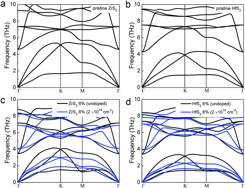 | ||
| Fig. 6 Phonon dispersion calculations of ZrS2 and HfS2 monolayers. (a) and (b) represent the unstrained states; (c) and (d) represent the strain at 6%. The black and blue lines present the undoped and hole doped states, respectively, where the hole densities are both around 2.0 × 1014 cm−2. | ||
4 Conclusions
In summary, using first-principle calculations, we have predicted the ferromagnetism of hole doped 1T-MX2 (M = Zr, Hf; X = S, Se) monolayers by strain engineering. Four pristine MX2 monolayers are nonmagnetic semiconductors with indirect band-gaps. We first demonstrate that hole doping induces tunable ferromagnetic properties in MX2 monolayer. This carrier-tunable magnetism is tightly correlated with the p orbital of S or Se atoms. When tensile strains are applied to dichalcogenides, the critical hole density can reduce to 5 × 1013 cm−2, and keep the ferromagnetic states till the hole density up to 3 × 1014 cm−2, which would attribute to the enlarged DOS near the Fermi energy. Moreover, the magnetism of fluorine doped ZrS2 monolayer is studied. Band structure shows that F_ZrS2 is a p-type semiconductor, which confirms the hole doping. The magnetic moment and spin-polarization energy indicate that fluorine doped ZrS2 monolayer can be modulated to stable magnetic states. The phonon dispersions of the strained ZrS2 and HfS2 monolayers indicate the structural stability by hole doping. Therefore, the hole doped MX2 monolayers will provide an achievable idea for 2D functional materials in spintronics.Conflicts of interest
There are no conflicts to declare.Acknowledgements
This work was supported by the Fundamental Research Funds for the Central Universities, a Project Funded by the Priority Academic Program Development of Jiangsu Higher Education Institutions (PAPD). We are grateful for the support of NSFC (51672126). The calculations were performed on parallel computers at the High Performance Computing Center (HPCC) of Nanjing University.References
- K. F. Mak, C. Lee, J. Hone, J. Shan and T. F. Heinz, Atomically thin MoS2: a new direct-gap semiconductor, Phys. Rev. Lett., 2010, 105, 136805 CrossRef PubMed
.
- J. N. Coleman, M. Lotya, A. O'Neill, S. D. Bergin, P. J. King, U. Khan, K. Young, A. Gaucher, S. De, R. J. Smith, I. V. Shvets, S. K. Arora, G. Stanton, H.-Y. Kim, K. Lee, G. T. Kim, G. S. Duesberg, T. Hallam, J. J. Boland, J. J. Wang, J. F. Donegan, J. C. Grunlan, G. Moriarty, A. Shmeliov, R. J. Nicholls, J. M. Perkins, E. M. Grieveson, K. Theuwissen, D. W. McComb, P. D. Nellist and V. Nicolosi, Two-Dimensional Nanosheets Produced by Liquid Exfoliation of Layered Materials, Science, 2011, 331, 568 CrossRef CAS PubMed
- K. F. Mak, K. He, J. Shan and T. F. Heinz, Control of valley polarization in monolayer MoS2 by optical helicity, Nat. Nanotechnol., 2012, 7, 494 CrossRef CAS PubMed
- X. Qian, J. Liu, L. Fu and J. Li, Quantum spin Hall effect in two-dimensional transition metal dichalcogenides, Science, 2014, 346, 1344–1347 CrossRef CAS PubMed
- Y. Saito, T. Nojima and Y. Iwasa, Highly crystalline 2D superconductors, Nat. Rev. Mater., 2016, 2, 16094 CrossRef
- G. Wang, A. Chernikov, M. M. Glazov, T. F. Heinz, X. Marie, T. Amand and B. Urbaszek, Colloquium: Excitons in atomically thin transition metal dichalcogenides, Rev. Mod. Phys., 2018, 90, 021001 CrossRef CAS
- J. Zhou, J. Lin, X. Huang, Y. Zhou, Y. Chen, J. Xia, H. Wang, Y. Xie, H. Yu, J. Lei, D. Wu, F. Liu, Q. Fu, Q. Zeng, C.-H. Hsu, C. Yang, L. Lu, T. Yu, Z. Shen, H. Lin, B. I. Yakobson, Q. Liu, K. Suenaga, G. Liu and Z. Liu, A library of atomically thin metal chalcogenides, Nature, 2018, 556, 355–359 CrossRef CAS PubMed
- Z. Hu, Z. Wu, C. Han, J. He, Z. Ni and W. Chen, Two-dimensional transition metal dichalcogenides: interface and defect engineering, Chem. Soc. Rev., 2018, 47, 3100–3128 RSC
- K. Xu, Z. Wang, F. Wang, Y. Huang, F. Wang, L. Yin, C. Jiang and J. He, Ultrasensitive Phototransistors Based on Few-Layered HfS2, Adv. Mater., 2015, 27, 7881–7887 CrossRef CAS PubMed
- L. Li, X. Fang, T. Zhai, M. Liao, U. K. Gautam, X. Wu, Y. Koide, Y. Bando and D. Golberg, Electrical Transport and High-Performance Photoconductivity in Individual ZrS2 Nanobelts, Adv. Mater., 2010, 22, 4151–4156 CrossRef CAS PubMed
- W. Zhang, Z. Huang, W. Zhang and Y. Li, Two-dimensional semiconductors with possible high room temperature mobility, Nano Res., 2014, 7, 1731–1737 CrossRef CAS
- X. Zhang, Z. Meng, D. Rao, Y. Wang, Q. Shi, Y. Liu, H. Wu, K. Deng, H. Liu and R. Lu, Efficient band structure tuning, charge separation, and visible-light response in ZrS2-based
van der Waals heterostructures, Energy Environ. Sci., 2016, 9, 841–849 RSC
- M. Zhang, Y. Zhu, X. Wang, Q. Feng, S. Qiao, W. Wen, Y. Chen, M. Cui, J. Zhang, C. Cai and L. Xie, Controlled Synthesis of ZrS2 Monolayer and Few Layers on Hexagonal Boron Nitride, J. Am. Chem. Soc., 2015, 137, 7051–7054 CrossRef CAS PubMed
- J. Coey, d0 ferromagnetism, Solid State Sci., 2005, 7, 660–667 CrossRef CAS
- H. Peng, H. Xiang, S.-H. Wei, S.-S. Li, J.-B. Xia and J. Li, Origin and enhancement of hole-induced ferromagnetism in first-row d0 semiconductors, Phys. Rev. Lett., 2009, 102, 017201 CrossRef PubMed
- A. Mielke and H. Tasaki, Ferromagnetism in the Hubbard model, Commun. Math. Phys., 1993, 158, 341–371 CrossRef
- Y. Ma, Y. Dai, M. Guo, C. Niu, Y. Zhu and B. Huang, Evidence of the existence of magnetism in pristine VX2 monolayers (X = S, Se) and their strain-induced tunable magnetic properties, ACS Nano, 2012, 6, 1695–1701 CrossRef CAS PubMed
- Y. Zhou, Z. Wang, P. Yang, X. Zu, L. Yang, X. Sun and F. Gao, Tensile strain switched ferromagnetism in layered NbS2 and NbSe2, ACS Nano, 2012, 6, 9727–9736 CrossRef CAS PubMed
- X. Feng, S. Lu, C. J. Pickard, H. Liu, S. A. T. Redfern and Y. Ma, Carbon network evolution from dimers to sheets in superconducting ytrrium dicarbide under pressure, Communications Chemistry, 2018, 1, 85 CrossRef
- T. Cao, Z. Li and S. G. Louie, Tunable magnetism and half-metallicity in hole-doped monolayer GaSe, Phys. Rev. Lett., 2015, 114, 236602 CrossRef PubMed
- B. Huang, H. L. Zhuang, M. Yoon, B. G. Sumpter and S.-H. Wei, Highly stable two-dimensional silicon phosphides: Different stoichiometries and exotic electronic properties, Phys. Rev. B: Condens. Matter Mater. Phys., 2015, 91, 121401 CrossRef
- H. Xiang, B. Xu, Y. Xia, J. Yin and Z. Liu, Strain tunable magnetism in SnX2 (X= S, Se) monolayers by hole doping, Sci. Rep., 2016, 6, 39218 CrossRef CAS PubMed
- Z. Liang, B. Xu, H. Xiang, Y. Xia, J. Yin and Z. Liu, Carrier-tunable magnetism in two dimensional graphene-like C2N, RSC Adv., 2016, 6, 54027–54031 RSC
- K. F. Mak, K. He, C. Lee, G. H. Lee, J. Hone, T. F. Heinz and J. Shan, Tightly bound trions in monolayer MoS2, Nat. Mater., 2012, 12, 207 CrossRef PubMed
- Y. Zhang, T. Oka, R. Suzuki, J. Ye and Y. Iwasa, Electrically switchable chiral light-emitting transistor, Science, 2014, 344, 725–728 CrossRef CAS PubMed
- S. Lu, W. Ma, G. Jin, Q. Zeng, X. Feng, T. Feng, H. Liu, S. Meng, S. A. T. Redfern and B. Yang, A combined experimental and theoretical investigation of donor and acceptor interface in efficient aqueous-processed polymer/nanocrystal hybrid solar cells, Sci. China: Chem., 2018, 61, 437–443 CrossRef CAS
- D. J. Late, L. Bin, L. Jiajun, Y. Aiming, H. S. S. R. Matte, G. Matthew, C. N. R. Rao and V. P. Dravid, GaS and GaSe ultrathin layer transistors, Adv. Mater., 2012, 24, 3549–3554 CrossRef CAS PubMed
- P. Manchanda, A. Enders, D. J. Sellmyer and R. Skomski, Hydrogen-induced ferromagnetism in two-dimensional Pt dichalcogenides, Phys. Rev. B, 2016, 94, 104426 CrossRef
- Y. Ma, Y. Dai, M. Guo, C. Niu, L. Yu and B. Huang, Strain-induced magnetic transitions in half-fluorinated single layers of BN, GaN and graphene, Nanoscale, 2011, 3, 2301–2306 RSC
- Y. Li, J. Kang and J. Li, Indirect-to-direct band gap transition of the ZrS2 monolayer by strain: first-principles calculations, RSC Adv., 2014, 4, 7396–7401 RSC
- J. Kang, H. Sahin and F. M. Peeters, Mechanical properties of monolayer sulphides: a comparative study between MoS2, HfS2 and TiS3, Phys. Chem. Chem. Phys., 2015, 17, 27742–27749 RSC
- G. Kresse and J. Hafner, Ab initio molecular dynamics for liquid metals, Phys. Rev. B: Condens. Matter Mater. Phys., 1993, 47, 558 CrossRef CAS
- G. Kresse and J. Furthmüller, Efficiency of ab initio total energy calculations for metals and semiconductors using a plane-wave basis set, Comput. Mater. Sci., 1996, 6, 15–50 CrossRef CAS
- G. Kresse and J. Furthmüller, Efficient iterative schemes for ab initio total-energy calculations using a plane-wave basis set, Phys. Rev. B: Condens. Matter Mater. Phys., 1996, 54, 11169 CrossRef CAS
- J. P. Perdew, K. Burke and M. Ernzerhof, Generalized gradient approximation made simple, Phys. Rev. Lett., 1996, 77, 3865 CrossRef CAS PubMed
- X. Gu and R. Yang, Phonon transport in single-layer transition metal dichalcogenides: A first-principles study, Appl. Phys. Lett., 2014, 105, 131903 CrossRef
- D. L. Greenaway and R. Nitsche, Preparation and optical properties of group IV–VI2 chalcogenides having the CdI2 structure, J. Phys. Chem. Solids, 1965, 26, 1445–1458 CrossRef CAS
- D. Çakır, F. M. Peeters and C. Sevik, Mechanical and thermal properties of h-MX2 (M = Cr, Mo, W; X = O, S, Se, Te) monolayers: A comparative study, Appl. Phys. Lett., 2014, 104, 203110 CrossRef
- K.-A. N. Duerloo, M. T. Ong and E. J. Reed, Intrinsic piezoelectricity in two-dimensional materials, J. Phys. Chem. Lett., 2012, 3, 2871–2876 CrossRef CAS
- X. Zhao, P. Chen, C. Xia, T. Wang and X. Dai, Electronic and magnetic properties of n-type and p-doped MoS2 monolayers, RSC Adv., 2016, 6, 16772–16778 RSC
Footnote |
| † Electronic supplementary information (ESI) available. See DOI: 10.1039/c9ra01218d |
| This journal is © The Royal Society of Chemistry 2019 |