
 Open Access Article
 This Open Access Article is licensed under a Creative Commons Attribution-Non Commercial 3.0 Unported Licence
Two-dimensional additive diethylammonium iodide promoting crystal growth for efficient and stable perovskite solar cells†
Xin Huang,
Qiuhong Cui *,
Wentao Bi,
Ling Li,
Pengcheng Jia,
Yanbing Hou,
Yufeng Hu,
Zhidong Lou and
Feng Teng*
*,
Wentao Bi,
Ling Li,
Pengcheng Jia,
Yanbing Hou,
Yufeng Hu,
Zhidong Lou and
Feng Teng*
Key Laboratory of Luminescence and Optical Information, Ministry of Education, Beijing Jiaotong University, Beijing 100044, China. E-mail: qhcui@bjtu.edu.cn; fteng@bjtu.edu.cn; Tel: +86 10 51684860
First published on 11th March 2019
Abstract
Methylammonium lead iodide perovskite photovoltaics have attracted remarkable attention due to their exceptional power conversion efficiencies (PCEs). The film morphology of organometallic halide perovskite plays a very important role in the performance of planar perovskite solar cells (PVSCs). Previous methods have been explored to control the crystal growth for getting a compact and smooth perovskite film. Here, we report an effective and reproducible approach for enhancing the stability and the efficiency of PVSCs by incorporating a small quantity of two-dimensional (2D) material diethylammonium iodide (DAI) in three-dimensional (3D) MAPbI3, which can facilitate the perovskite crystallization processes and improve the resulting film crystal quality. The fabricated (DA2PbI4)0.05MAPbI3 perovskite hybrid films exhibit good morphology with larger grains and uniform morphology. Simultaneously, reduced defects and enhanced carrier lifetime within a full device indicate enhanced crystallization effects as a result of the DAI inclusion. The photovoltaic device attains a high photocurrent of 22.95 mA cm−2 and a high fill factor of 79.04%, resulting in an overall PCE of 19.05%. Moreover, the stability of the 10% DAI doped perovskite solar cell is also improved. These results offer a promising stable and efficient light-absorbing material for solid-state photovoltaics and other applications.
Introduction
Organic–inorganic metal halide perovskite solar cells (PVSCs) represent a breakthrough for next generation thin-film optoelectronics due to their outstanding properties such as high absorption coefficient,1,2 long electron–hole diffusion lengths,3,4 tunable bandgap,5–7 and low-temperature processability,8 which bring about the promise of both high efficiency and low fabrication cost,3,9 and have already improved power conversion efficiency (PCE) from 3.8% to 23.7%.1,10 Theoretically speaking, the PVSCs may achieve an excellent PCE about 31% with high fill factor (FF) and open circuit voltage (VOC).11 Many strategies to improve the quality of perovskite films for high FF have been applied, including one-step spin coating,12 antisolvent dripping,13 two-step sequential deposition,14 vapor deposition,15 doctor blading16 and various improved strategies. Among them, a solution-processed perovskite film deposition procedure and antisolvent dripping method has become popular method, due to its fast film growth technique. The narrow processing window for properly adding the antisolvent makes it tricky to fabricate high quality perovskite film. For guaranteeing the improved morphology of the perovskites, additional operations like thermal treatment,17 solvent annealing,18 or using additives19–21 have been adopted. Several types of chemical additives, such as polymers,22 ionic liquids23 and ammonium salts24,25 can increase the performance of PVSC devices.Two-dimensional (2D) materials have become popular ammonium salts attributed to great tolerance to moist environment due to their unique structure characterized by hydrophobic groups which are combined with 3D perovskite in PVSCs.26,27 2D perovskites PEA2MA2Pb3I10 (PEA = C6H5(CH2)2NH3)28 and BA2MAn−1PbnI3n+1 (BA = CH3(CH2)3NH3, n = 2, 3, and 4),29 and quasi-2D perovskites PEA2MA59Pb60I181,30 and (BE)2(FA)8Pb9I28,31 (BE = C6H5CH2NH3) were used as active layers and significantly improved the moisture stability of PVSCs. The devices based on the above layered perovskite compounds exhibit a slightly lower PCE than the control device owing to the introduction of insulated spacer cations in the 3D perovskite lattice, which have strongly bound excitons with low mobility that may hamper the charge transport in perovskite films.28,29,32,33 Thus, recent attempts have been focused on introducing small quantity of two-dimensional (2D) materials to fabricate perovskite film.34,35 A small quantity of PEAI were used to fabricate (PEA2PbI4)0.017(MAPbI3) PVSCs with highly efficiency and long-term-stable, while the exist of PEA2PbI4 still lead to lower JSC than that of control device.34 PEAI doped PbI2 film (PEAI/PbI2 = 0.05) was used to react with MAI to fabricate highly efficient 2D/3D PVSCs with a high efficiency of 19.10%,35 while the low-pressure heating process need 2 hours and the particle size of the perovskite film is nonuniform. Recently, diethylammonium halogen ammonium salts (DAX, DA+ = (CH3CH2)2NH2+) have been used to improve the morphology of the active layer in PVSCs.36,37 Recently, ammonium salt diethylammonium hydrochloride used as an additive enabled to accelerate the growth of the perovskite film.36 While, only diethylammonium hydrochloride added in the precursor solution keeps non-stoichiometric ratio, and diethylammonium hydrochloride can volatilize out from the film during the growth of perovskite crystal, introducing the uniformity of crystals, smoothness of film surface, and therefore, leading to low FF and PCE. Two-dimensional (2D) material diethylammonium bromide has also been used in our previous work to post treat MAPbI3 film, and Br element can induce the small crystals secondary grow into large crystals.37 However, the performances of the device with post-annealed film are partly depend on the performances of the MAPbI3 film which cause a lower short circuit current. It is worth mentioning that doping of DA cations into the perovskite precursor solution may be beneficial to improve the film morphology and increase the short circuit current of the devices. And DA+ contains a short-branched chain than PEA+ and BA+ which may have better charge transport property and is able to introduce into the MAPbI3 perovskite to enhance the performance of the devices.
In this work, small quality of 2D perovskite DA2PbI4 (DAI is abbreviation for diethylammonium iodide, DA+ = (CH3CH2)2NH2+) has been incorporated with three-dimensional (3D) MAPbI3 in precursor solution, which facilitates the perovskite crystallization processes and improves the resulting film quality. The fabricated (DA2PbI4)0.05MAPbI3 perovskite hybrid films exhibit good morphology with larger grains more than 1 micro and without pinhole. Compared with control device, incorporated 2D perovskites DA2PbI4 with long alkyl chain can increase long term stability of the device. Applying the mixed (DA2PbI4)0.05MAPbI3 perovskite hybrid film in solar cells, the enhanced performance is achieved with a VOC of 1.05 V, short-circuit current (JSC) of 22.95 mA cm−2, and FF of 79.04%, leading to a remarkable efficiency of 19.05%, which is 20% higher than that of the control device (15.73%).
Results and discussion
Fig. 1a and b illustrates the diagram and energy level of the planar perovskite solar cells used in this work. The perovskite layer was fabricated by antisolvent assisted deposition method. A small quantity of 2D material DAI was incorporated in 3D MAPbI3 with different compositions by mixing different amounts of 1.25 M solution of DAI![[thin space (1/6-em)]](https://www.rsc.org/images/entities/char_2009.gif) :PbI2 (2:1) with the MAI:PbI2 precursor solution (DAI:MAI = 7%, 10% and 15% molar ratio), and denoted as 7%, 10% and 15% DAI contents for convenience. The chemical structure of DAI and schematic of DAI doped perovskite crystal are shown in Fig. 1c and d.
:PbI2 (2:1) with the MAI:PbI2 precursor solution (DAI:MAI = 7%, 10% and 15% molar ratio), and denoted as 7%, 10% and 15% DAI contents for convenience. The chemical structure of DAI and schematic of DAI doped perovskite crystal are shown in Fig. 1c and d.
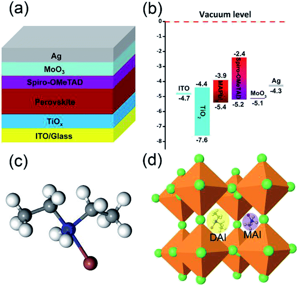 | ||
| Fig. 1 Structure (a) and energy level (b) diagram of the inverted planar perovskite solar cell, the chemical structure of DAI (c) and schematic of DAI doped perovskite crystal (d). | ||
The morphological evolution of perovskite films using various DA incorporation methods is shown in scanning electron microscopy (SEM) images (Fig. 2), indicating that incorporated DAI contents can positively facilitate the perovskite film grain growth. The morphology of the perovskite film without DAI was characterized by a poor-quality surface with small sized crystals about 161.54 nm. When the DAI content is 7%, the perovskite film presents larger grains with average grain size up to 0.71 μm. When the DAI content is 10%, the grains size of perovskite film presents much larger grains about 1.27 μm, resulting in a much denser and more homogeneous morphology than the MAPbI3 film. When the DAI content is 15%, the average grains size down to 1.00 μm. Generally, the larger the perovskite film crystals are, the better the solar cell performance is expected, because perovskite films with larger grains have lesser grain boundaries which act as barriers for charge transport between the cathode and anode in PVSCs.38,39 Therefore, from the SEM images, the 10% DAI incorporated perovskite film may be the most suitable for high performance devices. The above results exhibit that incorporating small quality of DAI in MAPbI3 precursor solution can facilitate the film crystallization and produce larger grains with more homogeneous grain-size distribution, and 10% DAI content can induce largest grain growth. Besides, in order to investigate whether other 2D cations incorporated can enlarge the perovskite grains, we also prepare the 10% PEAI and 10% BAI doped perovskite films for comparison. The SEM images of 10% PEAI and 10% BAI doped perovskite films are tested and displayed in Fig. S1.† It is obvious that the films doped with these two materials exhibit small grains less than 100 nm, and even smaller than the MAPbI3 film. The result demonstrate that DA cation doped 3D perovskite can increase the film crystal grains is its unique properties.
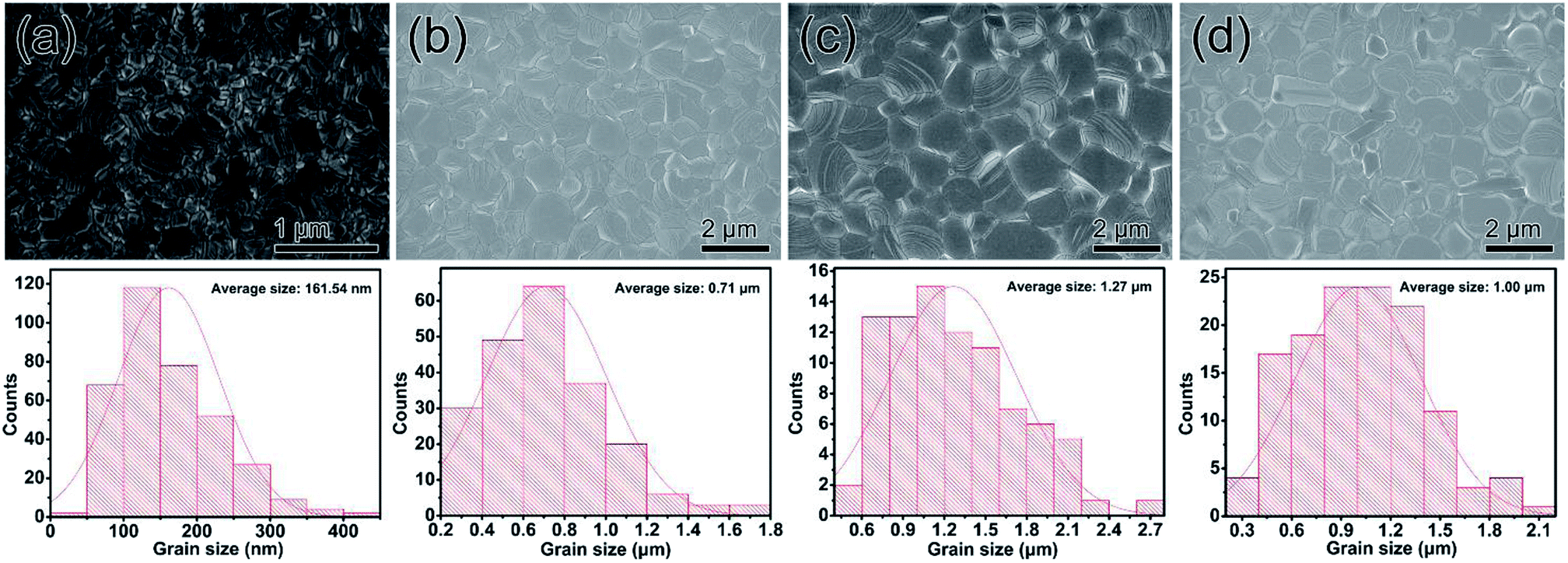 | ||
| Fig. 2 Top view of SEM images and correspond grain size of perovskite films without DA (a) and with 7% DAI content (b), 10% DAI content (c) and 15% DAI content (d). | ||
X-ray diffraction (XRD) analysis were carried out to identity a distinction of the perovskite films with different DAI contents, as shown in Fig. 3a. The MAPbI3 film exhibits the main characteristic diffraction peaks at the 2θ values of 14.13°, 28.46°, and 31.90° corresponding to the (110), (220), and (310) planes of tetragonal perovskite, respectively. The DA mixed perovskite film exhibits stronger diffusion peaks at (110) and (220) than those of DA free perovskite film, which reflects better crystallinity. Full width at half maximum (FWHM) of XRD peak corresponding to (110) plane is 0.08° for the 7% and 10% DAI contents, which is narrower than that of the film without DAI (0.10°), however, the FWHM is widened to be 0.09° for 15% DAI content. Those results indicate that the perovskite film incorporated 10% DAI content shown the best crystallinity. Furthermore, compared the XRD patterns of perovskite film of different DAI contents with the XRD patterns of 2D perovskite DA2PbI4 film in Fig. S2,† it can be confirmed that the several peaks around 7.5° in the XRD patterns of DA mixed films belong to DA2PbI4 and DA2PbI4 is successfully embedded in MAPbI3 film.
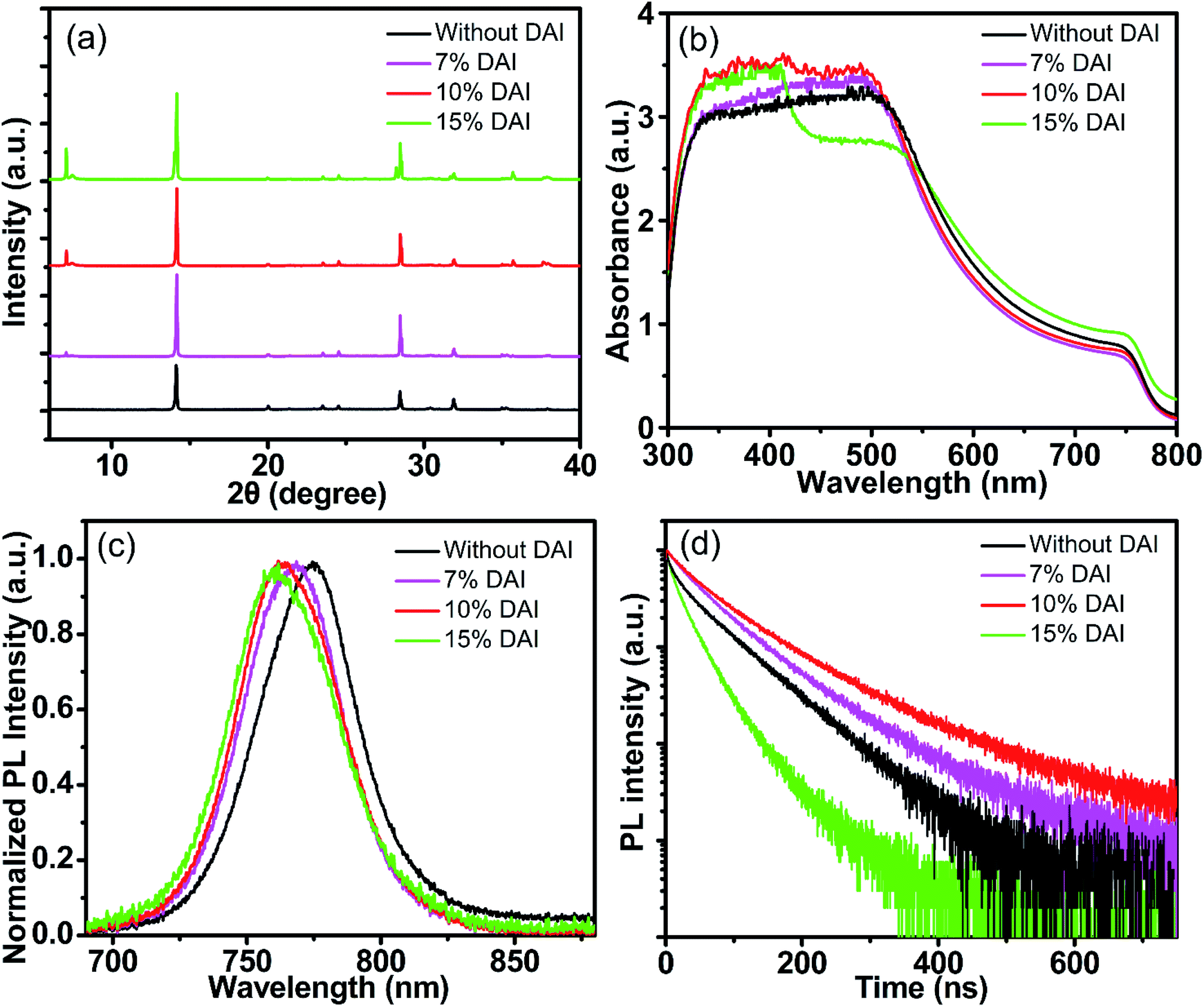 | ||
| Fig. 3 X-ray diffraction patterns (a), UV-vis absorption spectra (b), PL spectra (c) and TRPL spectra (d) of perovskite films without and with 7%, 10% and 15% DAI contents. | ||
To investigate the effects of DAI doping into MAPbI3 on its optical properties, UV-visible absorption spectroscopy and steady-state photoluminescence (PL) spectra were measured as shown in Fig. 3b and c. Apparently, the absorption is improved with low DAI contents (7% and 10%) and the absorption doesn't increase as the DAI content increases to 15%. The perovskite film with 10% DAI content exhibits best absorption, which may be associate with the best film morphology. The absorption edge of the DA mixed perovskite films presents only a slightly blue shift compared with that of the DAI free film, which is consistent with the blue-shifted emission peak in the PL spectrum in Fig. 3c. As presented, the DAI free perovskite film shows a PL peak at 774 nm, and DA incorporated perovskite films with 7%, 10% and 15% DAI contents exhibit blue-shifted PL peaks at 768, 764 and 761 nm. The slight shift to lower wavelength of the PL spectrum are probably due to the presence of 2D perovskite DA2PbI4.
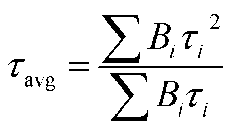
The time-resolved PL (TRPL) spectra were measured with the incident exciting light at 401 nm to examine the effect of DAI contents on nonradiative recombination in the perovskite films. The PL decay curves were fitted by the followed eqn (1) to evaluate the carrier recombination lifetime:40,41
|
y = A + B1exp(−t/τ1) + B2exp(−t/τ2)
| (1) |
 | (2) |
Considering large grains, well crystallinity and long lifetime of DAI incorporated films, current–voltage (J–V) measurements were employed to directly observe the effects of DAI contents on device performance. The J–V characteristics of the optimal devices with the DAI free and DAI mixed perovskite film under AM 1.5G illumination (100 mW cm−2) are shown in Fig. S3,† and the detailed device parameters are summarized in Table S1.† It is interesting to see that the VOC does not increase as the DAI content increases, which is different from the case of quasi-2D PEA2MAn−1PbnI3n+1.30,34 And the SEM image shows that the micron rods appeared on the surface of 15% DAI film, indicating the structural mismatch lead to different phases. These results illustrate that a small amount of 2D D2PbI4 is not incorporated into the crystal lattice of 3D MAPbI3 ascribe to the structural mismatch that possibly exists at the grain boundaries. The device based on the perovskite film with 10% DAI content shows the best PCE. Obviously, the device with the (DA2PbI4)0.05MAPbI3 perovskite film yields a significant enhancement in performance compared to the control device as shown in Fig. 4a and Table 1, mainly originating from a markedly enhanced FF from 68.60% to 79.04%, as well as a slightly increased JSC from 22.47 mA cm−1 to 22.95 mA cm−1 and VOC from 1.02 V to 1.05 V, leading to an overall PCE from 15.73% to 19.05%. The improved electronic properties of the device with the (DA2PbI4)0.05MAPbI3 perovskite film are normally ascribe to the large grains and less grain boundaries. J–V curves and statistical data of reverse and forward scanning are described in Fig. S4 and Table S2.† The J–V curves of MAPbI3 device yielded relatively high hysteresis. While, the hysteresis of the (DA2PbI4)0.05MAPbI3 perovskite solar cell is reduced compared with the DAI free device, which mainly attributed to increased grain size and decreased grain boundaries defects of the perovskite film.47
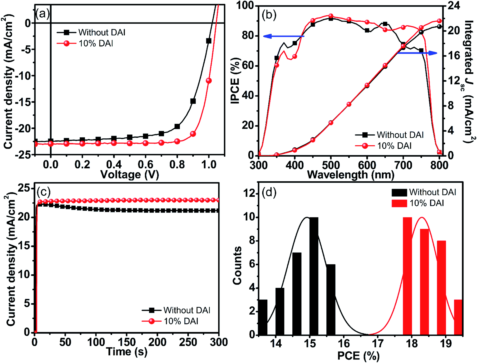 | ||
| Fig. 4 J–V characteristics (a), EQE spectra (b), stabilized short-circuit photocurrent density (c), and PCE distribution (d) of the perovskite devices without and with 10% DAI contents. | ||
| Active layer | JSC (mA cm−2) | VOC (V) | FF (%) | PCE (%) |
|---|---|---|---|---|
| Champion-MAPbI3 | 22.47 | 1.02 | 68.60 | 15.73 |
| MAPbI3 perovskite | (21.98 ± 0.48) | (1.02 ± 0.01) | (66.64 ± 1.82) | (14.92 ± 0.54) |
| Champion-DA doped | 22.95 | 1.05 | 79.04 | 19.05 |
| DA doped perovskite | (22.66 ± 0.44) | (1.04 ± 0.02) | (78.00 ± 1.65) | (18.30 ± 0.47) |
The incident photon-to-current efficiency (IPCE) spectra of the corresponding devices were measured, as shown in Fig. 4b. The (DA2PbI4)0.05MAPbI3 device exhibits a substantial enhancement in a broad wavelength range from 400 nm to 750 nm relative to the control device, which is consistent with the improvement in morphology and the increase in absorption. In addition, the value of the integrated photocurrent density from the IPCE for the solar spectrum is in well agreement with the obtained JSC. The output short-circuit photocurrent of the cells as a function of time were recorded, as shown in Fig. 4c. For the control device, the photocurrent is continuous decreased for the first 200 s, indicating that the device is unstable, which may be ascribe to the more traps in the perovskite film. While for the (DA2PbI4)0.05MAPbI3 devices, the photocurrent stabilizes within seconds to approximately 22.95 mA cm−2, which is comparable to the device parameters extracted from the J–V curve. The results proved that the (DA2PbI4)0.05MAPbI3 device better output stability which may be ascribed to the DAI induced large grains with less traps in the perovskite film. Fig. 4d displays the PCE distribution of the control devices and the (DA2PbI4)0.05MAPbI3 devices calculated from 30 devices, respectively. In general, the (DA2PbI4)0.05MAPbI3 devices exhibit an average PCE of 18.30%, which shows the good reproducibility for the (DA2PbI4)0.05MAPbI3 devices. Furthermore, we have also measured the long-term stability of the devices with DAI free perovskite film and (DA2PbI4)0.05MAPbI3 film which are storage in the glove box as shown in Fig. S5.† The PCE of the (DA2PbI4)0.05MAPbI3 device maintains almost 80% of the initial PCE after 60 days, showing better stability than the MAPbI3 device.
The cross-sectional SEM images of the MAPbI3 and (DA2PbI4)0.05MAPbI3 devices are shown in Fig. 5a and b. The perovskite layers are about 400 nm thick for both devices. It can be seen that the grains in the MAPbI3 device are about 100–300 nm and there are about two or more grains between the electronic transport layer and hole transport layer, which will bring out defects recombination. For the (DA2PbI4)0.05MAPbI3 device, the grains are large enough that most of the photogenerated charges can be collected by the electrodes without encountering grain boundaries, which can significantly decrease charge recombination loss and enhance the charge transport and carrier extraction. Meanwhile, the decreased grain boundary density might diminish the amount of boundary traps and bring about a reduction of defects recombination.
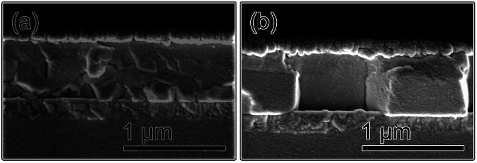 | ||
| Fig. 5 Cross-section SEM images of perovskite films without (a) and with 10% DAI content (b). | ||
To further explore the origin of the improved device characteristics, transient photocurrent (TPC) and transient photovoltage (TPV) techniques were carried out to further investigate the charge extraction and carrier recombination lifetimes in the working device.48,49 TPC was generated by a nanosecond pulse of a laser incident on devices and could provide insightful information on charge transport within the device. As shown in Fig. 6a, (DA2PbI4)0.05MAPbI3 based device shows a faster decay of 0.51 μs compared with that of the control device (1.08 μs), which confirms the (DA2PbI4)0.05MAPbI3 device has quicker charge transport and charge extraction.18 TPV, correlating to the electron lifetime in the active layer, provides an insight into carrier recombination in the cell. TPV measurement was performed with a pulsed laser under 1 sun illumination intensity at open-circuit voltage condition. As shown in Fig. 6b, the charge-recombination lifetime of the (DA2PbI4)0.05MAPbI3 device is 4.47 μs, much longer than 1.01 μs which is calculated from the control device. The longer carrier lifetime in the (DA2PbI4)0.05MAPbI3 device indicates that carrier recombination has been suppressed due to the better film quality.
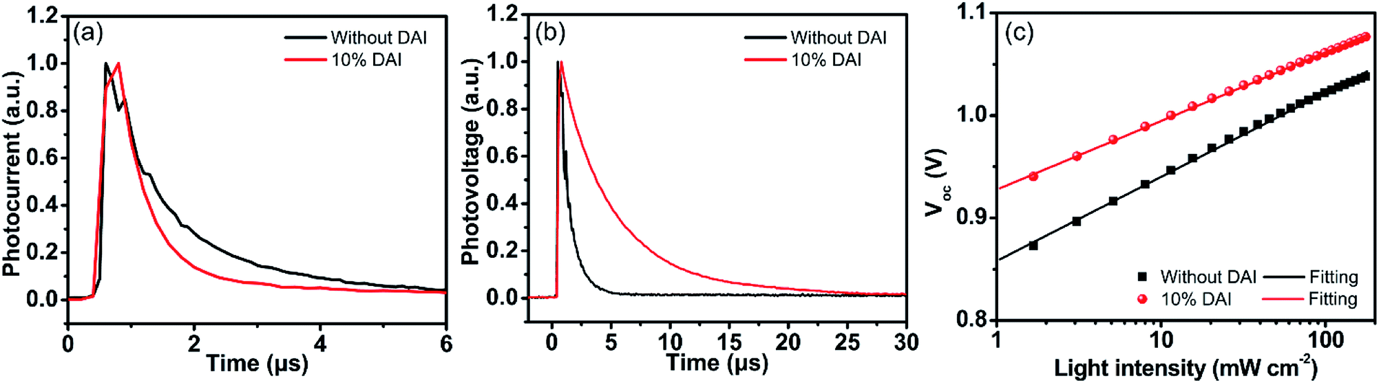 | ||
| Fig. 6 Transient photocurrent (a), transient photovoltage (b) and LIPV characteristics (c) of the perovskite devices without and with 10% DAI content. | ||
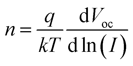
The open-circuit voltage as a function of light illumination intensities (LIPV) measurement was also performed to gain insight into the influence of traps on recombination under the open-circuit condition, as shown in Fig. 6c. The ideality factor (n) of PVSCs can be calculated according to equation:
Conclusions
In a summary, 2D perovskite DA2PbI4 was first incorporated into the 3D MAPbI3 perovskite to improve the crystallization of perovskite thin films. A significantly enhanced PCE (∼20%) of the planar perovskite solar cells is achieved from 15.73% to 19.05%. SEM images and XRD spectra evidence that incorporated 2D DA2PbI4 can facilitate homogenous crystal growth for better morphology and well crystallinity with large grains and uniform grains size. The grain size is large enough to throughout the device that can decrease charge loss by recombination at grain boundaries, which is also responsible for the improved performance. TRPL spectra were used to extract charge carrier dynamics, demonstrating an exceptional improvement in carrier lifetime for (DA2PbI4)0.05MAPbI3 film. The DAI doped perovskite film can effectively suppress trap-assisted recombination and enhance the charge extraction, which is evidenced from the TPC, LIPV and TPV measurements. This work provides an approach to obtain large grain perovskite films for high efficiency and stable perovskite solar cells.Experimental
Device fabrication
PbI2 (99.999%), MoO3 (99.998%) and Ag (99.99%) are purchased from Alfa Aesar. MAI and DAI are purchased from dyesol. Spiro-OMeTAD (99%) are purchased from 1-materials. The ITO substrates (15 Ω sq−1) were firstly cleaned in an ultrasonic bath by detergent, deionized water, acetone, and ethanol for 30 min each. Subsequently, the ITO substrates were exposed to UV-O3 plasma for 10 min. TiOx solution which were synthesized according to our previous work27 were deposited onto glass/ITO substrates with spin-coating speed at 7000 rpm for 40 s in ambient condition. The substrates were then annealed on a hot plate in ambient air at 150 °C for 40 min. The ITO substrates coated with the TiOx layers were transferred into a nitrogen-filled glove box. Subsequently, a 1.25 mM solution of MAPbI3 (PbI2:CH3NH3I = 1:1) in DMF was deposited onto TiOx layers by a one-step solvent induced method with the spin-coating process at 3000 rpm for 12 s followed by 5000 rpm for 30 s. During the low-speed step, 150 μl chlorobenzene was drop-casted on the rotating substrates after 8 s of spinning to promote crystallization. DA2PbI4 was incorporated in 3D MAPbI3 with different compositions by mixing different amounts of 1.25 M solution of DAI:PbI2 (2:1) with the MAI:PbI2 precursor solution (7%, 10% and 15% molar ratio). All the perovskite films were annealed at 100 °C for 10 min to form crystal film. After cooling down, 30 μl of spiro-OMeTAD solution were spin coated on the MAPbI3 layers at 4000 rpm for 30 s. Finally, about 10 nm MoO3 and 90 nm Ag were deposited on the tops of the spiro-OMeTAD-coated film at a constant evaporation rate of 0.1 Å s−1 and 1 Å s−1, respectively. The active area of all the devices is 4.5 mm2.
Film characterization
The morphologies of the perovskite films were investigated using a field emission scanning electron microscope (ZEISS GeminiSEM 300). The XRD patterns were tested with a Bruker D8 Advance X-ray diffractometer. The absorption spectra were measured using an UV-vis absorption spectrophotometer (Shimadzu UV-3101PC). The PL spectra of the perovskite films were examined using Fluorolog, Horiba Scientific. TRPL decay profiles of ITO/perovskite films detected by HORIBA JOBIN YVON using a 401 nm laser.Device characterization
J–V characteristics were measured using a solar simulator (SAN-EI Electric, XEC-301S) equipped with a Keithley 6430 Source meter under Air Mass 1.5 G illumination at 100 mW cm−2. The IPCE measurements were performed on a solar cell QE/IPCE measurement system (Zolix Solar Cell Scan 100). TPC and TPV measurements were conducted using a digital oscilloscope (Tektronix MSO 5104B), excitated by a Q-switched neodymium ion-doped yttrium aluminum garnet (Nd3+:YAG) laser. To form the short-circuit and open-circuit conditions, the input impedance of the oscilloscope was set to 50 Ω and 1 MΩ, respectively. The TPV measurement was carried out under 1 sun background illumination, with a laser pulse used to produce a small perturbation. The LIPV measurements were carried out using a focused cool white light emitting diodes (LEDs), for which illumination intensities were adjusted with a GPIB-controlled power. The VOC values were collected by a 16 bits data acquisition board (NI-6052E).Conflicts of interest
There are no conflicts to declare.Acknowledgements
This work was supported by the Fundamental Research Funds for the Central Universities (Grant No. 2018YJS183), and The National Key Research and Development Program of China (Grant No. 2016YFB0700703) and National Natural Science Foundation of China (Grant No. 51603010, 61775011, 61735004, 61674012, 61875009 and 61675018).Notes and references
- A. Kojima, K. Teshima, Y. Shirai and T. Miyasaka, J. Am. Chem. Soc., 2009, 131, 6050–6051 CrossRef CAS PubMed.
- J. H. Im, C. R. Lee, J. W. Lee, S. W. Park and N. G. Park, Nanoscale, 2011, 3, 4088–4093 RSC.
- W. S. Yang, J. H. Noh, N. J. Jeon, Y. C. Kim, S. Ryu, J. Seo and S. I. Seok, Science, 2015, 348, 1234 CrossRef CAS PubMed.
- N. J. Jeon, J. H. Noh, W. S. Yang, Y. C. Kim, S. Ryu, J. Seo and S. I. Seok, Nature, 2015, 517, 476–480 CrossRef CAS PubMed.
- J. H. Noh, S. H. Im, J. H. Heo, T. N. Mandal and S. I. Seok, Nano Lett., 2013, 13, 1764–1769 CrossRef CAS PubMed.
- M. M. Lee, J. Teuscher, T. Miyasaka, T. N. Murakami and H. J. Snaith, Science, 2012, 338, 643–647 CrossRef CAS PubMed.
- Y. Ogomi, A. Morita, S. Tsukamoto, T. Saitho, N. Fujikawa, Q. Shen, T. Toyoda, K. Yoshino, S. S. Pandey, T. Ma and S. Hayase, J. Phys. Chem. Lett., 2014, 5, 1004–1011 CrossRef CAS PubMed.
- P. W. Liang, C. Y. Liao, C. C. Chueh, F. Zuo, S. T. Williams, X. K. Xin, J. Lin and A. K. Jen, Adv. Mater., 2014, 26, 3748–3754 CrossRef CAS PubMed.
- D. Bi, C. Yi, J. Luo, J.-D. Décoppet, F. Zhang, S. M. Zakeeruddin, X. Li, A. Hagfeldt and M. Grätzel, Nat. Energy, 2016, 1, 16142 CrossRef CAS.
- NREL Chart, https://www.nrel.gov/pv/assets/pdfs/pv-efficiency-chart.20181214.pdf.
- W. E. I. Sha, X. Ren, L. Chen and W. C. H. Choy, Appl. Phys. Lett., 2015, 106, 221104 CrossRef.
- J. You, Z. Hong, Y. Yang, Q. Chen, M. Cai, T.-B. Song, C.-C. Chen, S. Lu, Y. Liu, H. Zhou and Y. Yang, ACS Nano, 2014, 8, 1674–1680 CrossRef CAS PubMed.
- N. J. Jeon, J. H. Noh, Y. C. Kim, W. S. Yang, S. Ryu and S. I. Seok, Nat. Mater., 2014, 13, 897–903 CrossRef CAS PubMed.
- J. Burschka, N. Pellet, S. J. Moon, R. Humphry-Baker, P. Gao, M. K. Nazeeruddin and M. Gratzel, Nature, 2013, 499, 316–319 CrossRef CAS PubMed.
- M. Liu, M. B. Johnston and H. J. Snaith, Nature, 2013, 501, 395–398 CrossRef CAS PubMed.
- Y. Deng, E. Peng, Y. Shao, Z. Xiao, Q. Dong and J. Huang, Energy Environ. Sci., 2015, 8, 1544–1550 RSC.
- T. Li, Y. Pan, Z. Wang, Y. Xia, Y. Chen and W. Huang, J. Mater. Chem. A, 2017, 5, 12602–12652 RSC.
- Z. Xiao, Q. Dong, C. Bi, Y. Shao, Y. Yuan and J. Huang, Adv. Mater., 2014, 26, 6503–6509 CrossRef CAS PubMed.
- J.-W. Lee, S.-H. Bae, Y.-T. Hsieh, N. De Marco, M. Wang, P. Sun and Y. Yang, Chem, 2017, 3, 290–302 CAS.
- X. Gong, M. Li, X.-B. Shi, H. Ma, Z.-K. Wang and L.-S. Liao, Adv. Funct. Mater., 2015, 25, 6671–6678 CrossRef CAS.
- M. Li, Y.-H. Chao, T. Kang, Z.-K. Wang, Y.-G. Yang, S.-L. Feng, Y. Hu, X.-Y. Gao, L.-S. Liao and C.-S. Hsu, J. Mater. Chem. A, 2016, 4, 15088–15094 RSC.
- L. Zuo, H. Guo, D. W. deQuilettes, S. Jariwala, N. De Marco, S. Dong, R. DeBlock, D. S. Ginger, B. Dunn, M. Wang and Y. Yang, Sci. Adv., 2017, 3, e1700106 CrossRef PubMed.
- J.-Y. Seo, T. Matsui, J. Luo, J.-P. Correa-Baena, F. Giordano, M. Saliba, K. Schenk, A. Ummadisingu, K. Domanski, M. Hadadian, A. Hagfeldt, S. M. Zakeeruddin, U. Steiner, M. Grätzel and A. Abate, Adv. Energy Mater., 2016, 6, 1600767 CrossRef.
- H.-L. Hsu, C.-C. Chang, C.-P. Chen, B.-H. Jiang, R.-J. Jeng and C.-H. Cheng, J. Mater. Chem. A, 2015, 3, 9271–9277 RSC.
- Y. Chen, Y. Sun, J. Peng, W. Zhang, X. Su, K. Zheng, T. Pullerits and Z. Liang, Adv. Energy Mater., 2017, 7, 1700162 CrossRef.
- G. Grancini, C. Roldan-Carmona, I. Zimmermann, E. Mosconi, X. Lee, D. Martineau, S. Narbey, F. Oswald, F. De Angelis, M. Graetzel and M. K. Nazeeruddin, Nat. Commun., 2017, 8, 15684 CrossRef CAS PubMed.
- B.-E. Cohen, M. Wierzbowska and L. Etgar, Sustainable Energy Fuels, 2017, 1, 1935–1943 RSC.
- I. C. Smith, E. T. Hoke, D. Solis-Ibarra, M. D. McGehee and H. I. Karunadasa, Angew. Chem., Int. Ed. Engl., 2014, 53, 11232–11235 CrossRef CAS PubMed.
- D. H. Cao, C. C. Stoumpos, O. K. Farha, J. T. Hupp and M. G. Kanatzidis, J. Am. Chem. Soc., 2015, 137, 7843–7850 CrossRef CAS PubMed.
- L. N. Quan, M. Yuan, R. Comin, O. Voznyy, E. M. Beauregard, S. Hoogland, A. Buin, A. R. Kirmani, K. Zhao, A. Amassian, D. H. Kim and E. H. Sargent, J. Am. Chem. Soc., 2016, 138, 2649–2655 CrossRef CAS PubMed.
- H. Zheng, G. Liu, L. Zhu, J. Ye, X. Zhang, A. Alsaedi, T. Hayat, X. Pan and S. Dai, Adv. Energy Mater., 2018, 8, 1800051 CrossRef.
- H. Tsai, W. Nie, J. C. Blancon, C. C. Stoumpos, R. Asadpour, B. Harutyunyan, A. J. Neukirch, R. Verduzco, J. J. Crochet, S. Tretiak, L. Pedesseau, J. Even, M. A. Alam, G. Gupta, J. Lou, P. M. Ajayan, M. J. Bedzyk and M. G. Kanatzidis, Nature, 2016, 536, 312–316 CrossRef CAS PubMed.
- Z. Wang, Q. Lin, F. P. Chmiel, N. Sakai, L. M. Herz and H. J. Snaith, Nat. Energy, 2017, 6, 17135 CrossRef.
- J. Chen, D. Lee and N. G. Park, ACS Appl. Mater. Interfaces, 2017, 9, 36338–36349 CrossRef CAS PubMed.
- M. H. Li, H. H. Yeh, Y. H. Chiang, U. S. Jeng, C. J. Su, H. W. Shiu, Y. J. Hsu, N. Kosugi, T. Ohigashi, Y. A. Chen, P. S. Shen, P. Chen and T. F. Guo, Adv. Mater., 2018, 30, e1801401 CrossRef PubMed.
- Y. Wang, N. Song, L. Feng and X. Deng, ACS Appl. Mater. Interfaces, 2016, 8, 24703–24711 CrossRef CAS PubMed.
- X. Huang, W. Bi, P. Jia, Y. Tang, Z. Lou, Y. Hu, Q. Cui, Y. Hou and F. Teng, Org. Electron., 2019, 67, 101–108 CrossRef CAS.
- C. Bi, Q. Wang, Y. Shao, Y. Yuan, Z. Xiao and J. Huang, Nat. Commun., 2015, 6, 7747 CrossRef CAS PubMed.
- Y. Shao, Y. Fang, T. Li, Q. Wang, Q. Dong, Y. Deng, Y. Yuan, H. Wei, M. Wang, A. Gruverman, J. Shield and J. Huang, Energy Environ. Sci., 2016, 9, 1752–1759 RSC.
- Q. Han, S. H. Bae, P. Sun, Y. T. Hsieh, Y. M. Yang, Y. S. Rim, H. Zhao, Q. Chen, W. Shi, G. Li and Y. Yang, Adv. Mater., 2016, 28, 2253–2258 CrossRef CAS PubMed.
- H. Si, Q. Liao, Z. Kang, Y. Ou, J. Meng, Y. Liu, Z. Zhang and Y. Zhang, Adv. Funct. Mater., 2017, 27, 1701804 CrossRef.
- P. Chen, Y. Bai, S. Wang, M. Lyu, J.-H. Yun and L. Wang, Adv. Funct. Mater., 2018, 1706923, DOI:10.1002/adfm.201706923.
- X. Xu, C. Ma, Y. Cheng, Y.-M. Xie, X. Yi, B. Gautam, S. Chen, H.-W. Li, C.-S. Lee, F. So and S.-W. Tsang, J. Power Sources, 2017, 360, 157–165 CrossRef CAS.
- D. Zhao, Y. Yu, C. Wang, W. Liao, N. Shrestha, C. R. Grice, A. J. Cimaroli, L. Guan, R. J. Ellingson, K. Zhu, X. Zhao, R.-G. Xiong and Y. Yan, Nat. Energy, 2017, 2, 17018 CrossRef CAS.
- D. Ramirez, K. Schutt, Z. Wang, A. J. Pearson, E. Ruggeri, H. J. Snaith, S. D. Stranks and F. Jaramillo, ACS Energy Lett., 2018, 3, 2246–2251 CrossRef CAS.
- N. De Marco, H. Zhou, Q. Chen, P. Sun, Z. Liu, L. Meng, E. P. Yao, Y. Liu, A. Schiffer and Y. Yang, Nano Lett., 2016, 16, 1009–1016 CrossRef PubMed.
- Y. Shao, Z. Xiao, C. Bi, Y. Yuan and J. Huang, Nat. Commun., 2014, 5, 5784 CrossRef CAS PubMed.
- H. Zhou, Q. Chen, G. Li, S. Luo, T.-b. Song, H.-S. Duan, Z. Hong, J. You, Y. Liu and Y. Yang, Science, 2014, 345, 542 CrossRef CAS PubMed.
- Q. Jiang, L. Zhang, H. Wang, X. Yang, J. Meng, H. Liu, Z. Yin, J. Wu, X. Zhang and J. You, Nat. Energy, 2016, 2, 16177 CrossRef.
- T. Kirchartz, F. Deledalle, P. S. Tuladhar, J. R. Durrant and J. Nelson, J. Phys. Chem. Lett., 2013, 4, 2371–2376 CrossRef CAS.
Footnote |
| † Electronic supplementary information (ESI) available. See DOI: 10.1039/c9ra01186b |
| This journal is © The Royal Society of Chemistry 2019 |