
 Open Access Article
 This Open Access Article is licensed under a Creative Commons Attribution-Non Commercial 3.0 Unported Licence
Direct chemical vapor deposition synthesis of large area single-layer brominated graphene†
Maria Hasanag,
Wang Meioubc,
Liu Yulianbc,
Sami Ullahbc,
Huy Q. Tabc,
Liang Zhaobc,
Rafael G. Mendese,
Zahida P. Malikg,
Nasir M. Ahmadh,
Zhongfan Liu a and
Mark H. Rümmeli*bcdef
a and
Mark H. Rümmeli*bcdef
aCollege of Chemistry & Molecular Engineering, Peking University, Beijing 100871, P. R. China
bCollege of Energy, Soochow Institute for Energy and Materials Innovations, Soochow University, Suzhou 215006, China
cKey Laboratory of Advanced Carbon Materials and Wearable Energy Technologies of Jiangsu Province, Soochow University, Suzhou, 215006, China
dInstitute of Environmental Technology, VŠB-Technical University of Ostrava, 17. Listopadu 15, Ostrava, 708 33, Czech Republic
eIFW Dresden, 20 Helmholtz Strasse, Dresden 01069, Germany. E-mail: m.ruemmeli@ifw-dresden.de
fCentre of Polymer and Carbon Materials, Polish Academy of Sciences, M. Curie-Sklodowskiej 34, Zabrze 41-819, Poland
gSchool of Natural Sciences, National University of Sciences and Technology, Islamabad 44000, Pakistan
hSchool of Chemical and Material Engineering, National University of Sciences and Technology, Islamabad 44000, Pakistan
First published on 1st May 2019
Abstract
Graphene and its derivatives such as functionalized graphene are considered to hold significant promise in numerous applications. Within that context, halogen functionalization is exciting for radical and nucleophilic substitution reactions as well as for the grafting of organic moieties. Historically, the successful covalent doping of sp2 carbon with halogens, such as bromine, was demonstrated with carbon nanotubes. However, the direct synthesis of brominated graphene has thus far remained elusive. In this study we show how large area brominated graphene with C–Br bonds can be achieved directly (i.e. a single step) using hydrogen rich low pressure chemical vapor deposition. The direct synthesis of brominated graphene could lead to practical developments.
1. Introduction
Since its isolation in 2004, graphene has been a center of attention because of its fascinating properties.1 However, currently many of the synthesis routes being actively pursued for graphene sheet production no longer generate pristine graphene; rather, graphene is covalently functionalized to tailor its chemical and physical properties towards certain applications.2,3 For example graphene oxide is much easier to process than pristine graphene due to its high solubility.4 Similarly, nitrogen functionalization has been shown to drastically increase the electrocatalytic activity of graphene.2 Bromine functionalization of graphene related materials like carbon nanotubes (CNTs) has been reported decades ago.5,6 Bromine functionalized CNTs have been demonstrated as a versatile precursor for covalent functionalization and as an efficient agent in gas sensing electrodes.7,8 Bromine is known to be an efficient leaving group in radical and nucleophilic substitution reactions that well suit grafting organic moieties such as polymer surfaces with OH, SH and NH2 functionalities.9 The bromine functionalized graphene has been demonstrated to induce properties such as p type doping,10–12 oxygen reduction reaction (ORR) activity,13 reversible bromine storing,14 sulphide ion detection15 and electrocatalytic decomposition of H2O2 in graphene.16 Besides, C–Br bonds are well suited for efficient grafting of organic moieties on graphene that can be used for various purposes, including electrochemical and electronic devices.17,18However, direct bromine functionalization of pristine graphene is relatively less known, mainly due to the chemically inert nature of pristine graphene.19 Moreover, the direct synthesis of Br doped graphene with C–Br bonds (as opposed to adsorbed Br2), thus far, has remained elusive. Most production routes for brominated graphene use indirect synthesis approaches and include thermal treatments,12 solution-phase synthesis,13 chemical bromination14 the plasma bromination of graphene,17 a halogen atmosphere during exfoliation of graphene oxide,18 post treatments of graphite bromide19 and CVD synthesized graphene.20 However, the indirect and multistep procedures to fabricate Br-doped graphene are time consuming (and thus typically more expensive), low yield and increase the risk of impurities in the final product beside the resultant materials are complex and only coarse control over product stoichiometry is achievable. Thus, there remains a crucial need to develop a facile approach for the direct and large-scale synthesis of Br-doped graphene. This will help pave the way to utilize brominated graphene in its various attractive applications at industrial level.
In light of these observations, we felt that it would be of interest to carry out large-area bromination of graphene via facile chemical vapor deposition (CVD) synthesis. The CVD growth of graphene on copper foil is particularly popular due to its distinct advantages such as easy transfer, large scale, and low cost.21 The catalytic growth mechanism on Cu foil surface in the CVD process allows different materials as graphene carbon and dopant source.22 We have established the first single-step CVD synthesis route for mono- and few- layer large graphene doped with bound bromine (C–Br bond), as opposed to adsorbed Br2. This was achieved using a single solid precursor of 1,2,5,6,9,10-hexabromocyclododecane in a H2 rich atmosphere as shown in Fig. 1a.
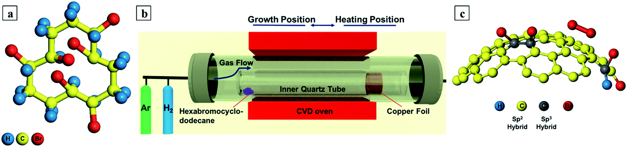 | ||
| Fig. 1 (a) Precursor (1,2,5,6,9,10-hexabromocyclododecane) stick and ball model (b) CVD set up and protocol (c) stick and ball model showing side view C–Br graphene (sp3-like bonding) and surface adsorbed Br2 (based on ref. 17). | ||
In our synthesis route, the precursor simultaneously serves as the source of C and Br. A hydrogen rich environment is chosen since H2 acts as a co-catalyst during the formation of active (surface bound) carbon species (CxHy)z required for efficient growth. In addition, it can etch away weak carbon–carbon bonds.23 Parametric studies with precursor zone temperature allow us to optimize for single-layer large area graphene. X-ray photoemission studies confirm the presence of C–Br bonding. Thus, our fabrication approach demonstrates the direct synthesis of brominated graphene by CVD is possible.
2. Materials and methods
2.1. Graphene growth
Bromine doped graphene was synthesized directly on a 25 μm thick copper substrate in a horizontal tube furnace at a pressure of 0.5 mbar. 1,2,5,6,9,10-Hexabromocyclododecane (Fig. 1a) was used as the source of both Br and C and was purchased from Haihang Industry Co., Ltd. And was used as received. 0.5 mg of this precursor powder was placed upstream (by the closed end of an inner reactor tube). The copper strip (45 × 10 mm) was rolled and carefully placed inside the inner reactor tube at a distance of 25 mm from its open end (opposite end to the precursor). This smaller quartz tube was then placed inside the main CVD furnace quartz tube as shown in Fig. 1b. The system was then evacuated to a pressure of 0.1 mbar with the help of a rotary pump. Afterwards, the system was flushed with pure Ar (99.99%) gas at a flow of 200 standard cubic centimeters per minute (SCCM) to reduce residual background gases. The Ar flushing was stopped after 30 minutes and switched to pure H2 (99.99%) flow at 16 sccm (at a pressure of 0.5 mbar). The furnace was heated to 1025 °C in 45 minutes. During heating, the oven remained at the copper foil (substrate) end of the inner quartz tube as indicated by heating position in Fig. 1b. Once the reaction temperature was reached, the CVD oven was slid towards the precursor end indicated by growth position in Fig. 1b to obtain the controlled evaporation of the precursor. The explored temperatures for the precursor were 150, 200, 250, 300 and 350 °C, where optimal growth was found at 200 °C for uniform monolayer graphene. The optimum growth time was 3 minutes. After growth the CVD oven was moved away from the reaction region to provide rapid cooling of the copper substrate and bring the reaction to a rapid stop.24 The hydrogen flow was stopped and switched back to 200 sccm of Ar until the furnace had cooled down to room temperature. A detailed graphical representation of the CVD protocol steps are shown in the ESI in Fig. S1.† Moreover, before starting every experiment the inner quartz tube was subsequently washed with acetone, ethanol and deionized water then blow dried with N2. Afterwards it was oxidized at 1025 °C for 30 minutes in the main CVD quartz tube to remove any source of contamination coming from the tube or the previous experiment.2.2. Transfer
The bromine-doped graphene was transferred on to standard lacey carbon Cu TEM grids for TEM and HRTEM studies. For that purpose, first the copper substrate was spin-coated with a PMMA solution in ethyl acetate, followed by its etching in 0.5 molar aqueous solution of ammonium persulphate (Sigma Aldrich, purity ≥ 98%) for ∼100 minutes. Thereafter it was rinsed thoroughly in deionized water. The film was then fished in deionized water onto a standard lacey carbon Cu TEM grid. The PMMA coating was removed in hot acetone vapor.25 Finally, to remove any organic residue that might have lifted, the TEM grid was annealed in high vacuum (10−6 mbar) at 200 °C for 12 hours.26For SEM and Raman characterizations, instead of a TEM grid SiO2 (300 nm)/Si wafer was used as the substrate for transfer. The wafer was sonicated in pure acetone followed by washing in absolute ethanol and then drying in N2. The graphene film was fished onto it and then annealed in an oven at 75 °C for 20 minutes. Afterwards, PMMA was removed by dipping it (for 2 minutes) in pure acetone.
2.3. Characterization
The large area brominated graphene was characterized through SEM on a Hitachi SU-8010. TEM and HRTEM characterization was performed on a Titan3 80–300 with an electron acceleration voltage of 80 kV. Raman spectra and mapping were collected on a Horiba (Confocal LabRAM HR 800) using 633 nm laser while keeping the laser power at 2 mW. XPS was performed on a Thermo Fisher Scientific (model ESCALAB 250 xi). The FTIR spectrum was recorded in the ATR mode on a Tensor 27 spectrometer from Bruker Optics. The sheet resistance was measured through a SZT-C four-probe test bench Suzhou Jingge electronics.3. Results and discussion
To synthesize our brominated graphene, a CVD reactor setup employing a half closed inner quartz tube configuration (Fig. 1b) was used. The use of the inner quartz tube configuration is helpful in trapping of reaction species that forms on decomposition of the precursor and allows their slow diffusion out of the reactor tube, thus provides sufficient time for graphene formation, in particular for powder precursors.27 With this set up even 0.5 mg of precursor material was enough to form large area brominated graphene. However, the rate at which the precursor sublimes and decomposes is affected by the precursor heating rate. Therefore, while the reaction zone (where the Cu substrate resides) was kept at a constant temperature of 1025 °C, different temperatures at the precursor heating zone were explored to optimize the reaction for the formation of (large area) monolayer brominated graphene. The growth time was maintained at 3 minutes.Precursor heating zone temperatures from 150 °C to 350 °C with 50 °C steps where explored. In all cases clear modes corresponding to sp2 carbon presence were observed (Fig. 2a–e). These modes are the D peak (∼1340 cm−1), the G peak (∼1580 cm−1) and the 2D mode (∼2700 cm−1) but with variation in their relative intensities.28 Moreover, for all the samples, the G band appeared at 1588 cm−1 with a slight upshift of 8 cm−1 and the 2D band appeared at 2642 cm−1 with a down shift of 58 cm−1 than the usual values concomitant with Br doping.12,29 This is further confirmed by presence of the D band presence that arise due to defects and doping from Br.29
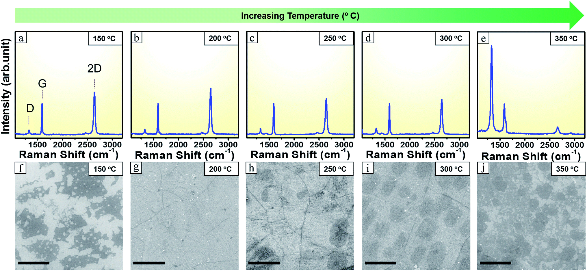 | ||
| Fig. 2 (a–e) Raman spectra recorded at the different precursor temperature. All spectra normalized w.r.t G mode (f–j) corresponding SEM images. Scale bar 5 μm. | ||
For all precursor heating temperatures, the 2D peak amplitude intensity is slightly larger than that for the G peak. In addition, the 2D peak is narrow (with a full width at half maximum (FWHM) of ca. 40 cm−1) indicating the presence of predominantly monolayer graphene.27 As one increases the precursor heating temperature the peaks in the Raman spectra show changes. For the precursor heating temperature of 150 °C the intensity of the 2D peak is comparatively lower. While measuring the graphene fragments, the signal was weak with large signal to noise ratio suggesting the graphene flakes were inhomogeneous. However, the 2D to G mode and the G to D ratio suggest the fragments are graphene (Fig. S2b†). By acquiring scanning electron micrographs from the samples one can obtain a better impression of the samples to further explain the Raman data. The SEM data in Fig. 2f suggests that when precursor was heated at 150 °C there was insufficient feedstock of active precursor species and thus continuous graphene layer could not be formed in this case. On increasing the precursor heating temperature further to 200 °C, the intensity of 2D band become higher and it was more symmetric. FWHM of 2D peak also got lower as compared to that of 150 °C Fig. S2a.† The corresponding SEM image in Fig. 2g shows continuous full coverage graphene. On increasing the precursor heating temperature to 250 °C the 2D band of Raman spectrum in Fig. 2c experienced an obvious decrease in its intensity and its FWHM also increased Fig. S2a.† The corresponding SEM image in Fig. 2h shows some secondary graphene islands forming over the initial graphene layer. Moreover, the precursor heating temperature at 300 °C resulted in corresponding increase in FWHM of the 2D peak Fig. S2a† although the change in 2D band intensity was negligible. The corresponding SEM image in Fig. 2i showed a regular patched structure of the grown graphene. This indicates that the flakes are becoming larger with rising precursor heating temperature. The Raman and SEM data fit will with each other. The D mode is present in all cases with a G/D of around 5 to 6 Fig. S2b.† The D mode is attributed to defects, including Br doping.30,31 The Raman spectroscopy data with the SEM micrographs shows that the optimum precursor zone temperature is at ca. 200 °C for large area homogenous single-layer graphene. Additionally a detailed Raman mapping data in Fig. S3.† from brominated single layer graphene was used to investigate the uniformity of the grown graphene.32 Raman maps were taken over 30 micrometer square area. The data shows that the brominated graphene is large area and crystalline.
On increasing the temperature further to 350 °C the corresponding 2D peak in Fig. 2e got wider, shorter and higher in its frequency (appearing at 2660 cm−1).28 Its FWHM value also increased to 63 cm−1 (Fig. S2a†) and was no longer symmetric. The G band also showed a small red shift of 2 cm−1 with the increased number of layers and appeared at 1586 cm−1.28 This indicated a multi-layer graphene formation. The D peak rose tremendously higher than both G and 2D peaks. The result was in agreement with the corresponding SEM image in Fig. 2j that shows a highly defective graphene. This can be attributed to the anisotropic etching effect of pure H2 that has become more dominant with increased precursor heating temperature.33
In case of the single-layer brominated graphene, further characterizations by transmission electron microscopy (TEM) were conducted as shown in Fig. 3. Low magnification studies show uniform large area deposition graphene in Fig. 3a. High resolution TEM (HRTEM) studies show that the graphene formed was predominantly monolayer. This was confirmed by forming holes (through electron beam irradiation)34 and visually confirming the layer number, as can be seen, for example, at the top left of Fig. 3b. Higher magnification studies of the material show a nicely crystalline honeycomb lattice concomitant with graphene in Fig. 3c. Moreover, the only one set of six fold symmetric SAED pattern also confirmed the monolayer nature of the brominated graphene in Fig. 3d and e.35
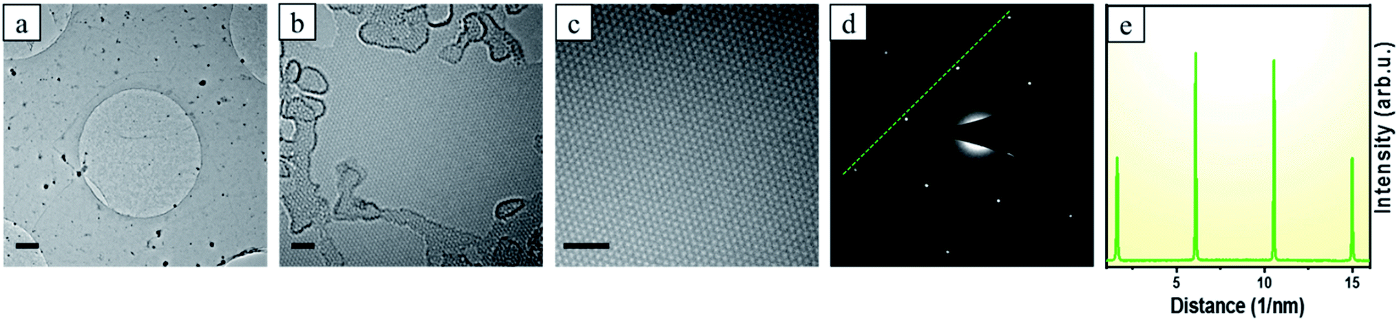 | ||
| Fig. 3 (a) TEM image shows large area deposition of the Br doped graphene. Scale bar 2 μm (b and c) HRTEM images showing the Br doped graphene is single layer. Scale bar 1 nm (d and e) SAED data and intensity profiles over the {1010} and outer {1120} reflexes showing the formed graphene is monolayer. The dark pointer in (d) is the shadow of the beam stop used to block the intense direct beam. | ||
To better comprehend the nature of the bromine doping in graphene, we conducted core level spectroscopy using X-ray photoemission spectroscopic (XPS). The low resolution long range survey spectrum in Fig. 4a reveals a predominant C 1s peak at 284.3 eV and additional peaks at 257 eV, 182 eV, 70.5 eV corresponding to the Br 3s, Br 3p, Br 3d.36,37 In addition, an O 1s signature at 531 eV and a Cu 2p peaks (at 933 eV) are observed.36,38 The atomic percentage of Br is ca. 3.5% while that for C is 49.7%. The O and Cu contributions, which are attributed to the substrate are 4.3% and 41.8%, respectively.39,40 The high resolution C 1s main peak in Fig. 4b can be fitted into three components centered at 284.3 eV, 285.1 eV and 286.5 eV that can be ascribed to C![[double bond, length as m-dash]](https://www.rsc.org/images/entities/char_e001.gif) C, C–C/C–H and C–O/C–Br respectively.36 The relative percentages of each of these three peaks are 43.7%, 25.9% and 30% respectively. The larges fraction is due to sp2 C (graphene), the second to a more sp3-like fraction with C/H and the lowest fraction due to C–Br.29
C, C–C/C–H and C–O/C–Br respectively.36 The relative percentages of each of these three peaks are 43.7%, 25.9% and 30% respectively. The larges fraction is due to sp2 C (graphene), the second to a more sp3-like fraction with C/H and the lowest fraction due to C–Br.29
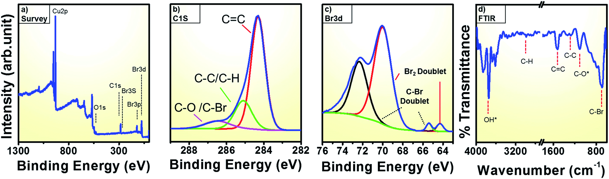 | ||
| Fig. 4 (a) Long range XPS survey spectrum for optimized precursor heating at 200 °C (b) high resolution C 1s spectrum (c) high resolution Br 3d spectrum (d) ATR spectrum in transmission mode. Adsorptions in ambient labelled with *. | ||
Furthermore, to show unequivocally that there is a C–Br fraction, we look in more detail at the Br 3d XPS response from bromine in Fig. 4c. Similar to previous studies on brominated CNTs two peak pairs are of observed here due to the different types of bromine bonds.29 A very weak doublet at the lower energies of 64.3 eV and 65.4 eV corresponds Br 3d5/2 lines. The doublet at higher energy with edges at 69.9 eV and 72.3 eV corresponds to Br 3d3/2 lines.29 Among each set of the doublet pairs the low lying peaks at 64.3 ± 0.2 and 69.9 ± 0.2 are assumed to arise from the physically adsorbed bromine derivatives such as carbon charge transfer Br2 complexes and BrH.41 Due to covalent bond formation between C and Br, a more stable and stronger interaction occurs and the high energy components at 65.4 ± 0.2 and 72.3 ± 0.2 is assigned to C–Br bond that confirms the formation of brominated graphene.29,42,43 The C–Br content was determined as 1.8% while the Br2 content is ca. 2% (error ±0.1%). The XPS data confirms the presence of a C–Br bond in the graphene. Indeed, the electrophilic addition of bromine across the graphene double bond changes the sp2 hybrid character to a more sp3-like geometry.17
We also examined the Cu data. The Cu 2p spectrum in Fig. S4a† from the Cu substrate shows the presence of shake up bands suggest there may be a little oxidized Cu (due to defects (e.g. grain boundaries or perhaps the bromination sites)).38 To better comprehend this we look at the O 1s spectrum (Fig. S4b†), which show two peaks at 529.8 eV and 531 eV can be attributed to Cu2O/CuO and C–O respectively.39,44 The respective atomic percentages for C–O and Cu2O/CuO are ca. 2.5% and 2.4%. This indicates that a small fraction of the brominated graphene is also oxidized. It is unclear if this occurs at defects sites after exposure to air or during synthesis.39,42
We additionally look at the functional groups of the brominated graphene with FTIR. In the FTIR spectrum (Fig. 4d) the peaks at ∼1250 cm−1 and ∼1100 can be attributed to C–C and C–O vibrations, respectively.45 The peak at ca. 1530 cm−1 is due to the CC stretching mode and appears as a strong peak.45,46 An intense peak at 690 cm−1 is attributed to C–Br and further supports the formation of brominated graphene.8,45,46 The absorption in the region from 3600 to 3700 cm−1 is due to surface adsorbed OH species from the ambient.46 The absorption due to C–H bond is assigned at 2987 cm−1.46 Thus, the XPS and FTIR data all confirm presence of covalently bonded Br. The FTIR data correlate very well with the XPS results.
Finally, we also examined the sheet resistance of the brominated graphene sheets, produced under different precursor heating temperature, using the four probe sheet resistance method. (Fig. S2c†) For the precursor heating temperature of 150 °C the sheet resistance cannot be measured due to absence of any continuous layer formation at this temperature. For the precursor heating temperatures of 200, 250 and 300 °C, the corresponding sheet resistance increased with increasing temperature. This can be correlated with SEM data where increasing the temperature led to the formation of additional secondary graphene layers as islands over the initial large area graphene. These additional islands provide scattering sties that thereby increase in the sheet resistance.47,48
4. Conclusions
In summary, we have developed the first direct, scalable and simple single step CVD process for large area, single layer, crystalline graphene with covalently doped bromine. We achieve this by using 1,2,5,6,9,10-hexabromocyclododecane as the powder precursor for Br and C species in a hydrogen rich environment. Indeed, this is the first report to show that direct synthesis of brominated graphene through CVD is possible. Moreover, the single solid precursor that acts as the elemental feedstock for both C and Br yields crystalline, large area and monolayer brominated graphene. The successful direct facile single step formation of brominated graphene by CVD thus offers a scalable pathway for the synthesis of a versatile spectrum of graphene derivatives suitable for a range of potential applications.14Conflicts of interest
There are no conflicts to declare.Acknowledgements
This work is supported by the National Science Foundation China (NSFC, Project 51672181), the National Science Center, Poland for the financial support within the frame of the Opus program (Grant agreement 2015/19/B/ST5/03399), the Czech Republic from ERDF “Institute of Environmental Technology – Excellent Research” (No. CZ.02.1.01/0.0/0.0/15_019/0000853). MHR thanks the Sino-German Research Institute for support (project: GZ 1400) and the start-up funding of the Suzhou Institute for Energy and Materials innovations (SIEMIS) and the School of Energy, Suzhou University.References
- K. S. Novoselov, A. K. Geim, S. V. Morozov, D. Jiang, M. I. Katsnelson, I. V. Grigorieva, S. V. Dubonos and A. A. Firsov, Nature, 2005, 438, 197–200 CrossRef CAS PubMed.
- A. J. Marsden, P. Brommer, J. J. Mudd, M. A. Dyson, R. Cook, M. Asensio, J. Avila, A. Levy, J. Sloan, D. Quigley, G. R. Bell and N. R. Wilson, Nano Res., 2015, 8(8), 2620–2635 CrossRef CAS.
- D. W. Boukhvalov and M. I. Katsnelson, J. Phys.: Condens. Matter, 2009, 21(34), 344205 CrossRef CAS PubMed.
- D. R. Dreyer, A. D. Todd and C. W. Bielawski, Chem. Soc. Rev., 2014, 43, 5288–5301 RSC.
- R. S. Lee, H. J. Kim, J. E. Fischer and A. Thess, Nature, 1997, 388, 255–257 CrossRef CAS.
- E. Unger, A. Graham, F. Kreupl, M. Liebau and W. Hoenlein, Curr. Appl. Phys., 2002, 2, 107–111 CrossRef.
- F. Hof, F. Hauke and A. Hirsch, Chem. Commun., 2014, 50, 6582–6584 RSC.
- D. Hines, M. H. Rummeli, D. Adebimpe and D. L. Akins, Chem. Commun., 2014, 50, 11568–11571 RSC.
- S. Wettmarshausen, G. Kuhn, G. Hidde, H. U. Mittmann and J. F. Friedrich, Plasma Processes Polym., 2007, 4, 832–839 CrossRef CAS.
- X. Fan, L. Liu, J.-L. Kuo and Z. Shen, J. Phys. Chem. C, 2010, 114, 14939–14945 CrossRef CAS.
- N. Jung, N. Kim, S. Jockusch, N. J. Turro, P. Kim and L. Brus, Nano Lett., 2009, 9, 4133–4137 CrossRef CAS PubMed.
- S. W. Chu, S. J. Baek, D. C. Kim, S. Seo, J. S. Kim and Y. W. Park, Synth. Met., 2012, 162, 1689–1693 CrossRef CAS.
- K. H. Wu, D. W. Wang, Q. Zeng, Y. Li and I. R. Gentle, Chin. J. Catal., 2014, 35, 884–890 CrossRef CAS.
- O. Jankovsky, P. Simek, K. Klimova, D. Sedmidubsky, S. Matejkova, M. Pumera and Z. Sofer, Nanoscale, 2014, 6, 6065–6074 RSC.
- S. Singh, K. Mitra, A. Shukla, R. Singh, R. K. Gundampati, N. Misra, P. Maiti and B. Ray, Anal. Chem., 2017, 89, 783–791 CrossRef CAS PubMed.
- S. Singh, M. Singh, K. Mitra, R. Singh, S. K. S. Gupta, I. Tiwari and B. Ray, Electrochim. Acta, 2017, 258, 1435–1444 CrossRef CAS.
- J. F. Friedrich, G. Hidde, A. Lippitz and W. E. S. Unger, Plasma Processes Polym., 2014, 34, 621–645 CrossRef CAS.
- H. L. Poh, P. Simek, Z. Sofer and M. Pumera, Chem.–Eur. J., 2013, 19, 2655–2662 CrossRef CAS PubMed.
- J. Zheng, H.-T. Liu, B. Wu, C.-A. Di, Y.-L. Guo, T. Wu, G. Yu, Y.-Q. Liu and D.-B. Zhu, Sci. Rep., 2012, 2, 662 CrossRef PubMed.
- A. E. Mansour, S. Dey and A. Amassian, ACS Appl. Mater. Interfaces, 2015, 7, 17692–17699 CrossRef CAS PubMed.
- X. Li, W. Cai, J. An, S. Kim, J. Nah, D. Yang, R. Piner, A. Velamakanni, I. Jung, E. Tutuc, S. K. Banerjee, L. Colombo and R. S. Ruoff, Science, 2009, 324, 1312–1314 CrossRef CAS PubMed.
- H. Wang, Y. Zhou, D. Wu, L. Liao, S. Zhao, H. Peng and Z. Liu, Small, 2013, 9(8), 1316–1320 CrossRef CAS PubMed.
- I. Vlassiouk, M. Regmi, P. Fulvio, S. Dai, P. Datskos, G. Eres and S. Smirnov, ACS Nano, 2011, 5, 6069–6076 CrossRef CAS PubMed.
- J. Seo, J. Lee, A. R. Jang, Y. Choi, U. Kim, H. S. Shin and H. Park, Chem. Mater., 2017, 29, 4202–4208 CrossRef CAS.
- H. Q. Ta, D. J. Perello, D. L. Duong, G. H. Han, S. Gorantla, V. L. Nguyen, A. Bachmatiuk, S. V. Rotkin, Y. H. Lee and M. H. Rümmeli, Nano Lett., 2016, 16, 6403–6410 CrossRef CAS PubMed.
- S. Gorantla, A. Bachmatiuk, J. Hwang, H. A. Alsalman, J. Y. Kwak, T. Seyller, J. Eckert, M. G. Spencere and M. H. Rummeli, Nanoscale, 2014, 6, 889–896 RSC.
- M. H. Rümmeli, S. Gorantla, A. Bachmatiuk, J. Phieler, N. Geißler, I. Ibrahim, J. Pang and J. Eckert, Chem. Mater., 2013, 25, 4861–4866 CrossRef.
- I. Childres, L. A. Jauregui, W. Park, H. Cao and Y. P. Chen, New Developments in Photon and Materials Research, Nova Science Publishers, Hauppauge NY, 2013 Search PubMed.
- L. G. Bulusheva, A. V. Okotrub, E. Flahaut, I. P. Asanov, N. P. Gevko, V. O. Koroteev, Yu. V. Fedoseeva, A. Yaya and C. P. Ewels, Chem. Mater., 2012, 24, 2708–2715 CrossRef CAS.
- M. H. Rummeli, A. Bachmatiuk, A. Scott, F. Borrnert, J. H. Warner, V. Hoffman, J. H. Lin, G. Cuniberti and B. Buchner, ACS Nano, 2010, 4, 4206–4210 CrossRef PubMed.
- J. F. Friedrich, S. Wettmarshausen, S. Hanelt, R. Mach, R. Mix, E. B. Zeynalov and A. Meyer-Plath, Carbon, 2010, 48, 3884–3894 CrossRef CAS.
- E. Auchter, J. Marquez, S. L. Yarbro and E. Dervishi, AIP Adv., 2017, 7, 125306 CrossRef.
- Y. Zhang, Z. Li, P. Kim, L. Zhang and C. Zhou, Anisotropic Hydrogen Etching of Chemical Vapor Deposited Graphene, ACS Nano, 2012, 6(1), 126–132 CrossRef CAS PubMed.
- L. Zhao, H. Q. Ta, A. Dianat, A. Soni, A. Fediai, W. Yin, T. Gemming, B. Trzebicka, G. Cuniberti, Z. Liu, A. Bachmatiuk and M. H. Rummeli, Nano Lett., 2017, 17, 4725–4732 CrossRef CAS PubMed.
- Q. Yu, L. A. Jauregui, W. Wu, R. Colby, J. Tian, Z. Su, H. Cao, Z. Liu, D. Pandey, D. Wei, T. F. Chung, P. Peng, N. P. Guisinger, E. A. Stach, J. Bao, S. S. Pei and Y. P. Chen, Nat. Mater., 2011, 10, 443–449 CrossRef CAS PubMed.
- J. F. Colomer, R. Marega, H. Traboulsi, M. Meneghetti, G. V. Tendeloo and D. Bonifazi, Chem. Mater., 2009, 21, 4747–4749 CrossRef CAS.
- J. Gao, F. Bao, Q. Zhu, Z. Tan, T. Chen, H. Cai, C. Zhao, Q. Cheng, Y. Yanga and R. Ma, Polym. Chem., 2013, 4, 1672–1679 RSC.
- V. Hayez, A. Franquet, A. Hubin and H. Terryn, Surf. Interface Anal., 2004, 36, 876–879 CrossRef CAS.
- J. Kwak, Y. Jo, S. D. Park, N. Y. Kim, S. Y. Kim, H. J. Shin, Z. Lee, S. Y. Kim and S. Y. Kwon, Nat. Commun., 2017, 8, 1–12 CrossRef CAS PubMed.
- P. R. Kidambi, B. C. Bayer, R. Blume, Z. J. Wang, C. Baehtz, R. S. Weatherup, M. G. Willinger, R. Schloegl and S. Hofmann, Nano Lett., 2013, 13, 4769–4778 CrossRef CAS PubMed.
- E. Papirer, R. Lacroix, J.-B. Donnet, G. Nanse and P. Fioux, Carbon, 1994, 32, 1341 CrossRef CAS.
- H. Au, N. Rubio and M. S. P. Shaffer, Chem. Sci., 2018, 9, 209–217 RSC.
- Y. Li, H. Chen, L. Y. Voo, J. Ji, G. Zhang, G. Zhang, F. Zhang and X. Fan, J. Mater. Chem., 2012, 22, 15021–15024 RSC.
- J. Zhang, C. Li, Z. Peng, Y. Liu, J. Zhang, Z. Liu and D. Li, Sci. Rep., 2017, 7, 4886 CrossRef PubMed.
- J. Coates and R. A. Meyers, Encyclopedia of Analytical Chemistry, John Wiley & Sons Ltd., Chichester, 2000 Search PubMed.
- Z. Xiaorong, L. Yanan, T. Chengan, Z. Hui, X. Lin and W. Jianfang, Mater. Res. Express, 2017, 4, 045601 CrossRef.
- F. Banhart, J. Kotakoski and A. V. Krasheninnikov, ACS Nano, 2010, 5, 26–41 CrossRef PubMed.
- T. O. Wehling, S. Yuan, A. I. Lichtenstein, A. K. Geim and M. I. Katsnelson, Phys. Rev. Lett., 2010, 105, 056802 CrossRef CAS PubMed.
Footnote |
| † Electronic supplementary information (ESI) available. See DOI: 10.1039/c9ra01152h |
| This journal is © The Royal Society of Chemistry 2019 |