DOI:
10.1039/C9RA01107B
(Paper)
RSC Adv., 2019,
9, 11737-11744
Development of moisture-proof polydimethylsiloxane/aluminum oxide film and stability improvement of perovskite solar cells using the film†
Received
12th February 2019
, Accepted 8th April 2019
First published on 15th April 2019
Abstract
A method for enhancing the moisture barrier property of polydimethylsiloxane (PDMS) polymer films is proposed. This is achieved by filling the PDMS free volume with aluminum oxide (AlOx). To deposit AlOx inside PDMS, thermal atomic layer deposition (ALD) is employed. The PDMS/AlOx film thus produced has a 30 nm AlOx layer on the surface. Its water vapor transmission rate (WVTR) is 5.1 × 10⁻³ g m−2 d−1 at 45 °C and 65% relative humidity (RH). The activation energy of permeability with the PDMS/AlOx film for moisture permeation is determined to be 35.5 kJ mol−1. To investigate the moisture barrier capability of the PDMS/AlOx layer, (FAPbI3)0.85(MAPbBr3)0.15/spiro-OMeTAD/Au perovskite solar cells are fabricated, and encapsulated by the PDMS/AlOx film. To minimize the thermal damage to solar cells during ALD, AlOx deposition is performed at 95 °C. The solar cells exposed to 45 °C-65% RH for 300 h demonstrate less than a 5% drop in the power-conversion efficiency.
Introduction
Recently, solar cell encapsulation employing organic–inorganic halide perovskite solar cells (PSCs) to overcome instability in the presence of moisture has gained considerable attention.1–4 Recently, various methods, such as using UV curable epoxy5 and moisture barrier film3,6 to protect the PSCs from moisture have been proposed, which show encouraging results under high humidity.7–11 The previous studies reported that encapsulated PSCs using an organic layer start degrading from perovskite decomposition when moisture penetrates the organic layer.5,12–14 To overcome this, atomic layer deposition (ALD) is used as one of the effective techniques to fabricate oxide thin films on the device. Furthermore, researchers reported the results of the water vapor transmission rate (WVTR) of oxide films fabricated by ALD. Wang et al. reported the use of ALD to fabricate Al2O3/MgO, which when coupled with solution-processed polymer, achieved a high moisture barrier and has a superior WVTR of 1.05 × 10⁻⁶ g m−2 d−1 at 60 °C-100% RH.15 Nam et al. obtained a WVTR of 2 × 10⁻³ g m−2 d−1 at 85 °C-85% RH using a composite layer of ALD Al2O3 and chemical-vapor-deposited graphene.16 We achieved a WVTR of 1.84 × 10⁻² g m−2 d−1 at 45 °C-100% RH when thermal ALD is used.17 Based on our previous research,17 a low process temperature of ALD and a method to enhance the WVTR are required to be used in PSCs. For low damage of PSCs during ALD, we performed ALD at a temperature as low as 95 °C. However, we observed that it is difficult to achieve the high moisture barrier property with a single Al2O3 film. Therefore, previous researchers employed organic materials to enhance the moisture barrier property. Park et al. introduced the thin film encapsulation method for OLED devices by coating polydimethylsiloxane (PDMS) on metal foil. They reported a WVTR of 4.4 × 10⁻⁴ g m−2 d−1 at 45 °C-40% RH.18 Similarly, Hong et al. introduced flexible lamination encapsulation using graphene films with PDMS on polyethylene terephthalate (PET).19 Liu et al. developed a hole transport material (HTM)-free PSC by using a carbon electrode and performing PDMS encapsulation. They reported long-term stability of PSCs in low-humidity conditions at room temperature for 3000 h.20 We summarized the related works in Table S1.† However, those results lacked the investigation of how the WVTR was increased using an organic layer. Therefore, first, we focused on a method to improve the moisture barrier property by combining PDMS and AlOx. Second, we investigated why the WVTR is enhanced when the PDMS/AlOx double layer is used. PDMS is employed because of its low cost,21 chemical stability,22 easy process to fabricate film or mold,23 high transparency,24 and common usage in the microfluidic cell25–27 and other devices.28,29 In addition, it exhibits the hydrophobic property.30 However, these results lack the investigation of how the WVTR was increased using an organic layer.
The objectives of the research reported in this study are: (1) to develop a method of enhancing the moisture barrier property of the PDMS by employing AlOx thin film; (2) to determine the WVTR of the PDMS/AlOx film by the Ca corrosion test, and to investigate the mechanism that improves the WVTR; (3) and to investigate the stability of PSCs encapsulated by the PDMS/AlOx moisture barrier film. Accordingly, we fabricated three types of films: (a) AlOx, (b) AlOx/PDMS, and PDMS/AlOx (Fig. S1†). To examine the effectiveness of the moisture barrier film, we encapsulated the perovskite solar cell, (FAPbI3)0.85(MAPbBr3)0.15/spiro-OMeTAD/Au, by these films.
Results and discussion
Effect of TMA and water pulse time on the deposition rate of AlOx thin film
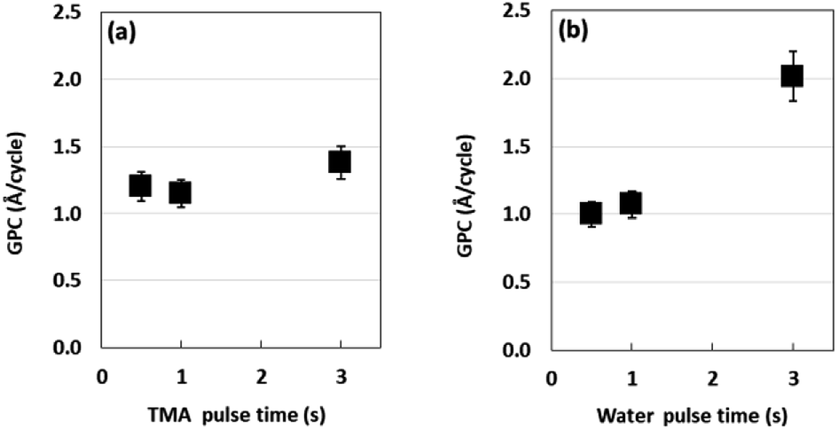
We investigated if TMA and water pulse times affect the growth rate of the AlOx film. Fig. 1a shows that the growth rate per cycle (GPC) of the AlOx film is in the 1.20–1.38 Å range with the change in TMA pulse time from 0.5 s to 3.0 s. Further, we examined the effect of water pulse time on the GPC of the AlOx film.
 |
| | Fig. 1 Effect of (a) TMA pulse time and (b) water pulse time on the growth rate of AlOx thin films. Si wafer substrates were used to form the AlOx thin film. The ALD process was performed at 95 °C for 100 cycles. | |
Fig. 2b shows that the GPC of the AlOx film doubled in 3 s water pulse time as compared to that obtained with 0.5 s water pulse time. This is attributed to precursor decomposition.31 Based on these results, we determined the GPC in accordance with the number of ALD cycles. Fig. 2a illustrates that the slope is 1.09 Å per cycle, which means the AlOx film grows linearly in a positive relationship with the ALD cycles. To examine the thickness, we employed transmission electron microscopy (TEM) and energy dispersive spectroscopy (EDS) analysis after 200 cycles (Fig. 2b and c). These figures indicate that the AlOx films formed uniformly on the substrate and consisted of Al and O. The presence of oxygen in the substrate is attributed to oxidation.32 Therefore, we observed that the thickness of AlOx films could be determined by changing the ALD cycles at fixed TMA and water pulse times.
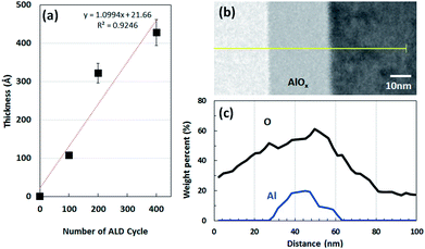 |
| | Fig. 2 (a) Thickness of AlOx thin films as a function of number of ALD cycles. (b) TEM image of 30 nm AlOx layer that is formed by using condition C in Table 1. (c) EDS element line scan results of the yellow line in (b). | |
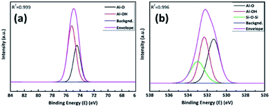
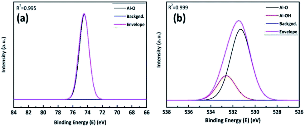
Once the AlOx thin films were formed by ALD process, we used an X-ray photoelectron spectra (XPS) to ensure the stoichiometric ratio of Al and O. Correlation factors (R2) of devolution fitting in Fig. 3(a) and (b) were 0.995, 0.999, respectively. Fig. 3a shows the Al 2p spectra of AlOx with Gaussian fitting. It is distributed by one component at the 74.45 eV, which corresponds to Al–O.32 Fig. 3b shows that the O 1s spectra of AlOx consist of two peaks, which correspond to Al–O and Al–OH bonds at 531.29 eV and 532.60 eV, respectively.33 On the base of peak devolution of each element, we determined the stoichiometric ratio of the fabricated film by ALD. We chose the peak area of Al–O bonding from the devolved Al 2p and O 1s spectra, and used the element-specific cross sections of Al 2p and O 1s.33,34 The results demonstrated that the stoichiometric ratio of [O/Al] was 1.38 (Table S3†)
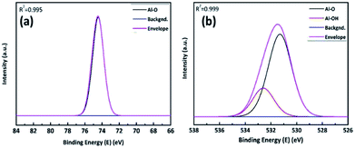 |
| | Fig. 3 XPS spectra of AlOx thin films on Si wafer. (a) Al 2p and (b) O 1s. | |
PDMS film filled with AlOx and its WVTR
Based on our previous study and other research findings,35–38 the AlOx thin film requires other layers for enhancing the moisture barrier property. For this experiment, we used PDMS as the organic layer. To cure a PDMS layer, it was heated at 95 °C for 1 h after spinning coating. This temperature corresponds to the temperature of ALD process. This allowed the PDMS to be cured further in the ALD chamber. The subsequent step was to deposit AlOx. After the formation of each layer, we examined the quality of the layer, especially the WVTR and contact angle.
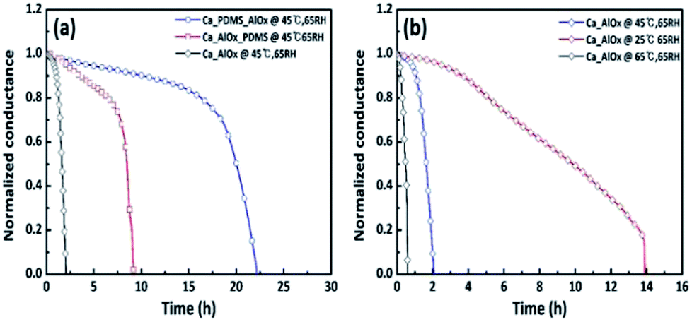
First, we investigated the effect of filling AlOx with free volume in PDMS on the WVTR. Fig. 4 show that the lag time of the Ca/PDMS/AlOx film was approximately twice as that of Ca/AlOx/PDMS, which are measured to be 19.71 h and 8.01 h, respectively. The WVTR values of the PDMS/AlOx and AlOx/PDMS film are determined to be 5.10 × 10⁻³ g m−2 d−1 and 1.46 × 10⁻² g m−2 d−1, respectively (refer Table 1). The WVTR value of a 30 nm AlOx film was determined to be 2.89 × 10⁻² g m−2 d−1, which is in good agreement with 1.84 × 10⁻² g m−2 d−1 (what we had done with AQUATRON model 2 (Mocon) before).17 Interestingly, the WVTR value was decreased by orders of 10−1 when we performed AlOx deposition on the PDMS layer. To examine the reason of enhancing the moisture barrier property, we employed TEM/EDS, ToF-SIMS, and XPS. First, we will explain the TEM results and then discuss the ToF-SIMS and XPS results.
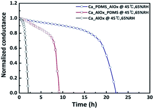 |
| | Fig. 4 Ca conductance test encapsulated by three types of materials: AlOx, PDMS/AlOx, and AlOx/PDMS. This test was conducted at 45 °C and 65% RH. | |
Table 1 Calculated WVTR and lag time of AlOx, AlOx/PDMS, and PDMS/AlOx at 45 °C and 65% RH
| Sample |
WVTR (g m−2 d−1) |
Lag time (h) |
| AlOx |
2.89 × 10⁻² |
0.86 |
| AlOx/PDMS |
1.46 × 10⁻² |
8.01 |
| PDMS/AlOx |
5.10 × 10⁻³ |
19.71 |
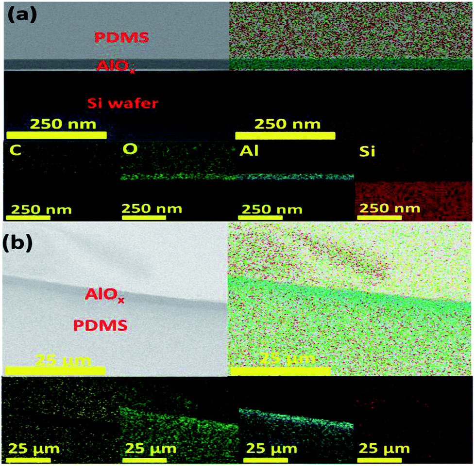
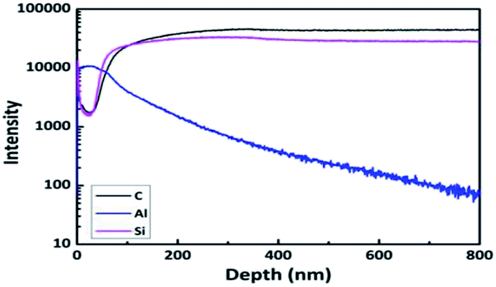
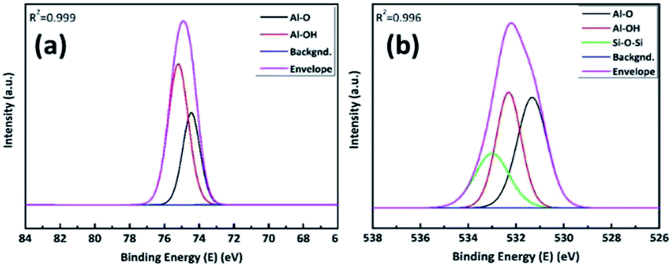
For the Si/AlOx/PDMS sample (Fig. 5a), EDS mapping results showed clear distinctions in the AlOx and the PDMS layers. Moreover, for the Si/PDMS/AlOx sample (Fig. 5b), Al was detected in the PDMS layer. We employed TOF-SIMS to analyze the elements inside the PDMS layer more precisely. Fig. 6 shows that Al exists from the surface to several hundred nanometers. To make sure that Al exists in the PDMS layer, we performed XPS analysis. Fig. 7a and b can be devaluated with Gaussian fitting whose correlation factors were 0.999 and 0.996 each. Fig. 7a illustrates the binding energy of Al 2p of the PDMS/AlOx film. The spectra was obtained at 74.45 eV and 75.2 eV, which represents Al–O and Al–OH bonds, respectively.32 Interestingly, unlike the Al 2p peak of AlOx reference, the peak area of the Al–OH bond for PDMS/AlOx occupies in the total 2p peak. The diffusivity and miscibility of the ALD precursor is related to the free volume of polymer,39 reactive site of polymer,40 and polymer porosity and crystallinity.41,42 These results are affected by the intrinsic property of the PDMS such as its crystallinity and reactivity43 and are similar to those of polyethylene ethoxylate (PEIE), whose semi-crystalline nature affects the retarded nucleation of the ALD layer.44 Fig. 7b shows the O 1s spectra of the PDMS/AlOx film. The Al–O spectra and Al–OH were detected at 531.29 eV and 532.60 eV, which are from the AlOx layer. As shown in Fig. S4,† the peak related to AlOx layer, where the peak between 3400 cm−1 and 3000 cm−1 were attributed to stretching vibrations of Al–OH45 and the peak of 1000 cm−1 was corresponded to Al–O stretching vibrations.46 The other spectra peak of 533.0 eV represent the binding energies of O–Si–O.47 These spectra peaks is from the PDMS layer supported by results from FTIR (Fig. S4†), which shows the peak at 1090 cm−1 were attributed to Si–O–Si stretching vibration in PDMS bone structure.48 An AlOx cluster forms in the void inside the PDMS layer during ALD process.39,44,49,50 Therefore, our results demonstrated that the moisture barrier property of the PDMS/AlOx film was improved by filling the free volume in PDMS layer with AlOx.
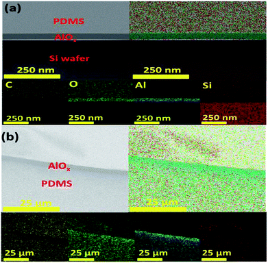 |
| | Fig. 5 TEM images and EDS elemental mapping (C, O, and Al, Si) of (a) AlOx/PDMS and (b) PDMS/AlOx. | |
 |
| | Fig. 6 ToF-SIMS depth profile of Si/PDMS/AlOx. | |
 |
| | Fig. 7 Si/PDMS/AlOx XPS spectra of (a) Al 2p and (b) O 1s. | |
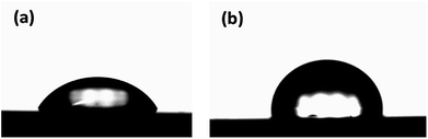
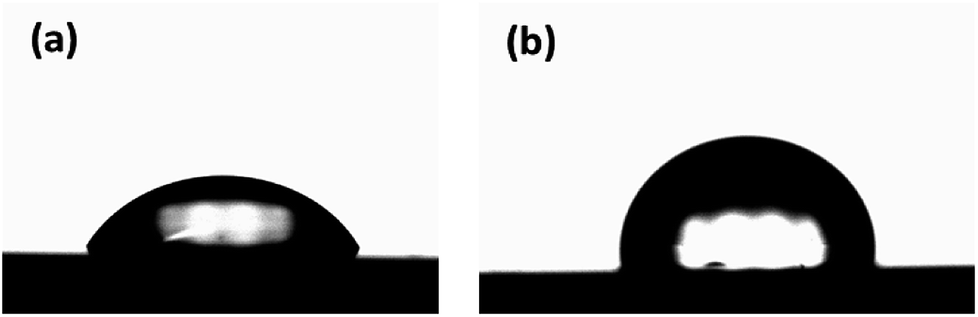
Second, we investigated the effect of AlOx and PDMS on surface properties, such as contact angle and surface tension.51 The permeation of water molecules is related to the wettability of the barrier thin film. Fig. 8 shows that the hydrophobicity was improved by forming the PDMS layer on the AlOx thin film. The contact angle and surface tension of the AlOx/PDMS sample was determined to be 86.8° and 30.0 mN m−1, respectively (refer Table 2). These results are attributed to the chemical structure of PDMS, which have the methyl functional group.52 Interestingly, the contact angle of AlOx increased from 60.8 to 74.1 when PDMS was used in the lower layer of the AlOx thin film. In general, the surface energy is concerned with the atom arrangement of surface and inside, which means that the measured contact angle indicates the growth formation of films according to the deposition condition.53 Therefore, the difference of surface energy with PDMS/AlOx indicated that the surface and internal arrangements of AlOx changed via deposition on PDMS, which corresponded with TEM-EDS and SIMS results.
 |
| | Fig. 8 Contact angles of (a) Si/AlOx and (b) Si/AlOx/PDMS using water. | |
Table 2 Contact angle and surface tension of Si/AlOx, Si/AlOx/PDMS and Si/PDMS/AlOx
| Sample |
DI [°] |
CH2I2 [°] |
Polar [mN m−1] |
Disp. [mN m−1] |
Surface tension [mN m−1] |
| AlOx |
60.8 |
47.8 |
17.1 |
27.0 |
44.1 |
| AlOx/PDMS |
86.8 |
58.8 |
3.9 |
26.1 |
30.0 |
| PDMS/AlOx |
74.1 |
58.4 |
10.8 |
23.5 |
34.2 |
Effect of temperature on the WVTR of PDMS/AlOx thin film
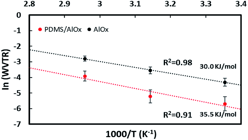
The WVTR value is dependent on the temperature and relative humidity.54,55 To examine the relationship between temperature and WVTR values, the Ca/AlOx and Ca/PDMS/AlOx samples were stored at three different temperatures: 25 °C, 45 °C, and 65 °C. The RH was maintained at 65%. The change in conductance was also monitored. Fig. 9 shows that the lag time increases as the temperature decreases to 25 °C. The result demonstrated that the moisture passage through the film was slow at low temperature. To quantify the moisture barrier property, the WVTR values were determined under each condition (see Table 3). In addition, we determined the activation energy of permeability of the Ca/AlOx and Ca/PDMS/AlOx films for permeation as using the following equation.55,56| | |
WVTR = WVTRo × exp(−Ea/RT),
| (1) |
where WVTRo is a constant dependent on the system, Ea is the activation energy for permeation, and R is the gas constant (8.314 J K−1 mol−1). The activation energy was determined using the linear slope from the graph of ln![[thin space (1/6-em)]](https://www.rsc.org/images/entities/char_2009.gif) WVTR versus 1/RT. The activation energies of permeability and correlation factors (R2) of AlOx and PDMS/AlOx were determined to be 30.0 kJ mol−1 (R2 = 0.98) and 35.5 (R2 = 0.91) kJ mol−1, respectively, as shown in Fig. 10. The activation energy of the PDMS/AlOx film is greater than that of AlOx film, which indicates it takes longer time for moisture permeation through the PDMS/AlOx film than AlOx film.57–60
WVTR versus 1/RT. The activation energies of permeability and correlation factors (R2) of AlOx and PDMS/AlOx were determined to be 30.0 kJ mol−1 (R2 = 0.98) and 35.5 (R2 = 0.91) kJ mol−1, respectively, as shown in Fig. 10. The activation energy of the PDMS/AlOx film is greater than that of AlOx film, which indicates it takes longer time for moisture permeation through the PDMS/AlOx film than AlOx film.57–60
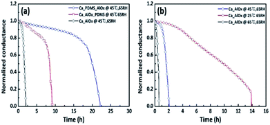 |
| | Fig. 9 Ca electrical test results of (a) PDMS/AlOx and (b) AlOx at 65% RH in accordance with the temperature. | |
Table 3 Contact angle and surface tension of Si/AlOx, Si/AlOx/PDMS and Si/PDMS/AlOx
| Sample |
WVTR (g m−2 d−1) |
Lag time (h) |
Measurement condition |
| PDMS/AlOx |
3.11 × 10⁻³ |
32.29 |
25 °C and 65% RH |
| PDMS/AlOx |
5.10 × 10⁻³ |
19.71 |
45 °C and 65% RH |
| PDMS/AlOx |
2.18 × 10⁻² |
9.16 |
65 °C and 65% RH |
| AlOx |
1.35 × 10⁻² |
6.01 |
25 °C and 65% RH |
| AlOx |
2.89 × 10⁻² |
0.86 |
45 °C and 65% RH |
| AlOx |
6.10 × 10⁻² |
0.26 |
65 °C and 65% RH |
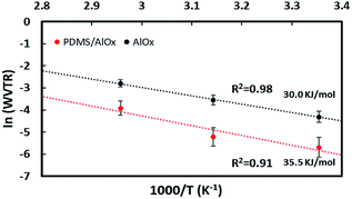 |
| | Fig. 10 Plots of the ln(WVTR) versus temperatures for AlOx and PDMS/AlOx. | |
PDMS/AlOx encapsulation for PSCs
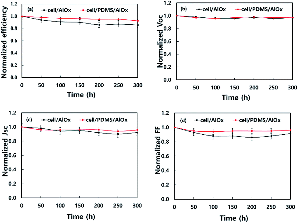
Finally, we fabricated the (FAPbI3)0.85(MAPbBr3)0.15/spiro-OMeTAD/Au solar cells, which are encapsulated by two kinds of films: (a) AlOx and (b) PDMS/AlOx. The solar cells were subjected to environmental test to examine their stabilities in terms of changes in power conversion efficiency (PCE). Although AlOx-and encapsulated solar cells suffered over 15% drop in PCE (see Fig. S2† for the degradation), but there were only below 5% PCE drop for the PDMS/AlOx-encapsulated devices at 45 °C in 65% RH for 300 h as shown in Fig. 11. This result shows better long-term stabilities compared to our previous report.61
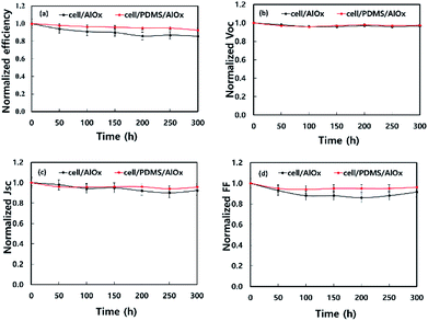 |
| | Fig. 11 Evolution of (a) PCE, (b) Voc, (c) Jsc and (d) fill factor of perovskite photovoltaic cells with AlOx or PDMS/AlOx at 45 °C and 65% RH condition. Error bar is standard deviation. | |
To investigate the main cause of the degradation in our devices, we conducted further experiment at room temperature in 65% RH condition with our PDMS/AlOx-encapsulated devices. As shown in Fig. S5,† the PDMS/AlOx encapsulated PSCs were rarely degraded even though these perovskite cells were exposed in high humidity at room temperature. It should be noted that the perovskite cells with PDMS/AlOx encapsulation layer showed PCE drop about 5% at 45 °C in 65% RH. Therefore, the main degradation mechanism on our devices is likely thermal degradation at spiro-OMeTAD layer as also reported in other literature.61 In other words, These results indicate that the PDMS/AlOx layer is effective in preventing moisture, but there are still rooms to investigate in the future for finding a good hole transport layer candidate to ensure long-term stability of perovskite solar cells.
Conclusions
This study focused on a method to enhance the moisture barrier property and WVTR of the AlOx thin film using PDMS. In addition, this study demonstrated the use of PDMS/ALD 30 nm AlOx layer on top of PSCs as an encapsulant to improve the stability by preventing moisture ingress. We observed that AlOx filled the vacancy in the PDMS layer when the AlOx thin films formed on the PDMS layer via ALD. That makes it difficult for moisture to permeate the film, which results in the enhancement of moisture barrier property. We deposited three types of thin films on the Ca film to examine the moisture barrier property. These include (a) AlOx, (b) AlOx/PDMS, and (c) PDMS/AlOx. The WVTR values of PDMS/30 nm AlOx layers by optimized thermal ALD process at a temperature as low as 95 °C was measured to be 5.1 × 10⁻³ g m−2 d−1 at 45 °C-65% RH. The activation energies for moisture permeation of the AlOx and PDMS/AlOx films were determined to be 30.0 kJ m−1 and 35.5 kJ mol−1, respectively. We observed that the PDMS/AlOx film was more hydrophobic than the AlOx film. This is attributed to the low surface tension of PDMS film. Finally, we fabricated the (FAPbI3)0.85(MAPbBr3)0.15/spiro-OMeTAD/Au perovskite solar cells and encapsulated it by two types of thin films. These include AlOx and PDMS/AlOx. The PDMS/AlOx-encapsulated solar cells experienced less than 8% drop in PCE after 300 h of 45 °C-65% RH. In contrast, the AlOx-encapsulated devices showed over 15% drop of PCE at 45 °C-65% RH. This is mainly attributed to thermal degradation of spiro-OMeTAD. With further development in the moisture barrier property of the AlOx film by employing the PDMS layer, we propose that the ALD process is an excellent approach to encapsulate perovskite solar cells.
Experimental section
Experimental apparatus
In this experiment, we designed an ALD system that is connected to a glove box. A thermal evaporator was installed inside the glove box, which can handle calcium (Ca) in a nitrogen condition. We formed the Ca layer on a glass using thermal evaporator, and then coated the PDMS on the Ca layer using a spin coater (Ca/PDMS). After curing the PDMS, the samples were placed in the ALD chamber to deposit AlOx. The whole process was performed in nitrogen environment. Each condition of this experiment is explained in detail in the next section.
Ca cell fabrication and characterization
Ca cell fabrication. The 300 nm Ca film was formed on a glass substrate (2.5 cm × 2.5 cm) using thermal evaporator. After Ca deposition, the 200 nm Al electrode was deposited onto the glass via evaporator (Fig. 1a). The next step is to encapsulate the Ca samples. For this, the Ca samples were divided into three groups, as shown in Fig. 1. These include (a) AlOx deposition (Ca/AlOx), (b) AlOx deposition and then PDMS coating (Ca/AlOx/PDMS), and (c) PDMS coating and then AlOx deposition (Ca/PDMS/AlOx). PDMS (Sylgard 184, Sigma Aldrich) was used in this study. The silicone elastomer was mixed with a curing agent in a 10:1 ratio by weight. The PDMS was coated at 1000 rpm for 30 s. Further, it was annealed at 95 °C for 1 h. The thickness of PDMS was measured to be about 55 μm(see Fig. S3†).
ALD deposition condition. We employed a thermal ALD process (model: IH-10, ITECHU, South Korea) in this study. The ALD procedure consists of four steps: (1) the TMA precursor was pulsed into reaction chamber, (2) Ar gas was purged to clean the reaction chamber, (3) H2O reactant was pulsed into reaction, and (4) excess reactant was removed from reaction chamber by Ar purging. To make sure of deposition thickness of AlOx, we investigated the effect of two factors on the deposition rate: (1) TMA pulse time and (2) water pulse time. The test conditions are summarized in Table S2.† Further, we examined the relationship between ALD cycles and AlOx thickness.
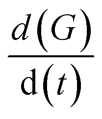
Characterization of Ca cell. The Ca cells were placed in three different temperature–humidity conditions: (a) 25 °C-65% RH, (b) 45 °C-65% RH, and (c) 65 °C-65% RH. The change in conductance (G) was measured in each condition (Keithley 2400 multimeter). Using the change in G, we determined the WVTR values using the equation stated in ref. 62.| |
 | (2) |
where 2 is the molar equivalent of Ca corrosion reaction, MH2O (18 g mol−1) and MCa (40.1 g mol−1) are the molecular weights of water and Ca, respectively, ρCa (1.55 g cm−3) is the density of Ca, σ (3.4 × 10⁻⁸ Ω m) is the resistivity of Ca,  is the rate of conductance (G) change, ACa is the area of deposited Ca, and A is the barrier film area on Ca.
Perovskite solar cell fabrication and characterization
Materials.
(1) Synthesis of perovskite absorption materials. (a) To synthesize HC(NH2)2I, 15 g formamidine acetate and 30 ml HI (57 wt% in water) were mixed in 100 ml ethanol at 0 °C for 2 h. After reacting the solution of HC(NH2)2I was dried with rotary evaporator at 50 °C for 1 h The white crystals were obtained following recrystallization from ethanol and washing with diethyl ether. (b) To obtain CH3NH3Br, the mixture solution of 11 ml methylamine (33 wt% in water) and 10 ml HBr (48 wt% in water) were stirred in 100 ml ethanol at 0 °C for 2 h.
(2) Preparation of perovskite absorption solutions. To prepare 1.2 M HC(NH2)2PbI3 solution, HC(NH2)2I and PbI2 were dissolved at room temperature in dimethylformamide (DMF):dimethyl sulfoxide mixed solvent (1:0.25 (v/v)). To fabrication of CH3NH3Br solution, the sequence of work was the same manner as described above. After preparing of base solution, 0.85 ml of HC(NH2)2PbI3 and 0.15 ml of CH3NH3Br3 solution were mixed to obtain (HC(NH2)2PbI3)0.85(CH3NH3PbBr3)0.15 mixed solution and extra PbI2 (5 mol% to HC(NH2)2PbI3) were added heating at 60 °C for 30 min.
Fabrication of perovskite solar cells. The used photovoltaics devices were fabricated with the following structures, FTO/c-TiO2/m-TiO2/perovskite/sprio-OMeTAD/Au. The procedure for cleaning the substrate included sonication and rinsing in distilled water, acetone, and isopropyl alcohol. About 50 nm of compact TiO2 (c-TiO2) was deposited by spray pyrolysis with 20 mM titanium diiopropoxide bis(acetylacetonate) solution at 450 °C on FTO substrate. 150 mg ml−1 of mesoporous TiO2 (m-TiO2, Dysol 30 NR-D) in ethanol was coated at 5000 rpm (acceleration of 2000 rpm s−1) for 10 s and heated 100 °C for 10 min. After process, the substrate was sintered at 500 °C for 30 min. The mixed perovskite solution described above was spin-coated at 2000 rpm (acceleration of 200 rpm s−1) for 10 s followed by 6000 rpm (acceleration of 2000 rpm s−1) for 30 s. During the last 20 s of the second coating steps, the cholorobenzene (CB), which works as anti-solvent, dropped. The perovskite film was heated at 100 °C for 20 min. A solution including 41.6 mg of spiro-OMeTAD, 7.5 μL of 500 mg ml−1 lithium bis(trfluoromethylsulphonyl)-imide (Li-TFSI) in acetonitrile (ACN) and 16. 9 μL of 4-tert-butylpyridine (tBP) in 0.5 ml of CB was dropped and coated on the perovskite layer at 2000 rpm (acceleration of 1200 rpm s−1) for 20 s. 100 nm of Au contacts were formed sequentially by vacuum deposition.
Characterization and stability test of PSCs. The film thickness of AlOx was measured using a spectroscopic ellipsometer (model: Elli-SE). To confirm the crystallinity of the film, the determined X-ray diffraction (XRD) patterns were measured using XRD-6100 (SHIMADZU, JAPAN) with a Cu Kα radiation source (λ = 0.1541 nm) at 30 kV and 30 mA. X-ray photoelectron spectroscopy (XPS) was performed using (Thetaprobe XPS, Thermo-Fisher Scientific) with Al Kα source at 15 kV to analyze the chemical bonding and composition of the film. The measured XPS data was calibrated using C 1s peak with 284.6 eV. The contact angle and surface tension values were measured with Phoenix 300 from SEO Co., Ltd., using DI and diiodomethane. The surface energy was determined by the Owen–Wendt equation using two measuring liquids.63| | |
γL(1 + cosθ) = 2(γdSγdL)1/2 + (γpSγpL)1/2,
| (3) |
where θ is the measured contact angle of the measuring liquid on the surface, the dispersion and polarity components of water are γdL = 22.85 dyn cm−1 and γpL = 50.3 dyn cm−1, respectively, and the components of diiodoemethane are γdL = 48.5 dyn cm−1 and γpL = 2.3 dyn cm−1To perform TEM, samples mounted on Cu girds were fabricated using a focused ion beam. The prepared sample was measured with JEM-2100F (JEOL Ltd) operating at 200 kV equipped with EDS (TEM 250, Oxford Instruments). The current density–voltage measurements were obtained by the solar cell testing system (LAB 200, McScience, Korea) including simulated solar light (AM 1.5G) with an intensity of 100 mW cm−2 using the K3000 model (McScience) and recorder using the ADCMT 6244 source measure unit. After masking with 0.075 cm2 aperture, the solar cells were measured at a scan rate of 1.2 V s−1. All the results were obtained under ambient conditions. The illumination intensity was calibrated using a standard Si reference cell (K801S-K067, McScience, Korea). The perovskite solar cell stability test was conducted at 45 °C-65% RH (TH401HA, ETAC, Japan).
Conflicts of interest
There are no conflicts to declare.
Acknowledgements
This research was supported by the Technology Development Program to Solve Climate Changes of the National Research Foundation (NRF) funded by the Ministry of Science and ICT (No. 2017M1A2A2048905), and the New & Renewable Energy of the Korea Institute of Energy Technology Evaluation and Planning (KETEP) grant funded by the Ministry of Trade, Industry and Energy (MOTIE) (No. 20173010012970).
Notes and references
- J. H. Noh, S. H. Im, J. H. Heo, T. N. Mandal and S. I. Seok, Nano Lett., 2013, 13, 1764–1769 CrossRef CAS PubMed.
- J. M. Frost, K. T. Butler, F. Brivio, C. H. Hendon, M. Van Schilfgaarde and A. Walsh, Nano Lett., 2014, 14, 2584–2590 CrossRef CAS PubMed.
- J. Cao, J. Yin, S. Yuan, Y. Zhao, J. Li and N. Zheng, Nanoscale, 2015, 7, 9443–9447 RSC.
- T. Leijtens, G. E. Eperon, N. K. Noel, S. N. Habisreutinger, A. Petrozza and H. J. Snaith, Adv. Energy Mater., 2015, 5, 1500963 CrossRef.
- Y. Han, S. Meyer, Y. Dkhissi, K. Weber, J. M. Pringle, U. Bach, L. Spiccia and Y.-B. Cheng, J. Mater. Chem. A, 2015, 3, 8139–8147 RSC.
- H. Kim, K.-G. Lim and T.-W. Lee, Energy Environ. Sci., 2016, 9, 12–30 RSC.
- X. Dong, X. Fang, M. H. Lv, B. C. Lin, S. Zhang, J. N. Ding and N. Y. Yuan, J. Mater. Chem. A, 2015, 3, 5360–5367 RSC.
- L. Shi, T. L. Young, J. Kim, Y. Sheng, L. Wang, Y. F. Chen, Z. Q. Feng, M. J. Keevers, X. J. Hao, P. J. Verlinden, M. A. Green and A. W. Y. Ho-Baillie, ACS Appl. Mater. Interfaces, 2017, 9, 25073–25081 CrossRef CAS PubMed.
- S. N. Habisreutinger, T. Leijtens, G. E. Eperon, S. D. Stranks, R. J. Nicholas and H. J. Snaith, Nano Lett., 2014, 14, 5561–5568 CrossRef CAS PubMed.
- A. Y. Mei, X. Li, L. F. Liu, Z. L. Ku, T. F. Liu, Y. G. Rong, M. Xu, M. Hu, J. Z. Chen, Y. Yang, M. Gratzel and H. W. Han, Science, 2014, 345, 295–298 CrossRef CAS PubMed.
- I. Hwang, I. Jeong, J. Lee, M. J. Ko and K. Yong, ACS Appl. Mater. Interfaces, 2015, 7, 17330–17336 CrossRef CAS PubMed.
- H. C. Weerasinghe, Y. Dkhissi, A. D. Scully, R. A. Caruso and Y.-B. Cheng, Nano Energy, 2015, 18, 118–125 CrossRef CAS.
- Q. Dong, F. Liu, M. K. Wong, H. W. Tam, A. B. Djurišić, A. Ng, C. Surya, W. K. Chan and A. M. C. Ng, ChemSusChem, 2016, 9, 2597–2603 CrossRef CAS PubMed.
- F. Matteocci, L. Cinà, E. Lamanna, S. Cacovich, G. Divitini, P. A. Midgley, C. Ducati and A. Di Carlo, Nano Energy, 2016, 30, 162–172 CrossRef CAS.
- L. Wang, C. Ruan, M. Li, J. Zou, H. Tao, J. Peng and M. Xu, J. Mater. Chem. C, 2017, 5, 4017–4024 RSC.
- T. Nam, Y. J. Park, H. Lee, I.-K. Oh, J.-H. Ahn, S. M. Cho, H. Kim and H.-B.-R. Lee, Carbon, 2017, 116, 553–561 CrossRef CAS.
- E. Y. Choi, J. Kim, S. Lim, E. Han, A. W. Ho-Baillie and N. Park, Sol. Energy Mater. Sol. Cells, 2018, 188, 37–45 CrossRef CAS.
- M.-H. Park, J.-Y. Kim, T.-H. Han, T.-S. Kim, H. Kim and T.-W. Lee, Adv. Mater., 2015, 27, 4308–4314 CrossRef CAS PubMed.
- H.-K. Seo, M.-H. Park, Y.-H. Kim, S.-J. Kwon, S.-H. Jeong and T.-W. Lee, ACS Appl. Mater. Interfaces, 2016, 8, 14725–14731 CrossRef PubMed.
- Z. Liu, B. Sun, T. Shi, Z. Tang and G. Liao, J. Mater. Chem. A, 2016, 4, 10700–10709 RSC.
- X. Ling, C. Ser Choong, C. S. Premachandran, D. Pinjala and M. K. Iyer, 7th Electronic Packaging Technology Conference (EPTC), 2005, vol. 1, p. 5 Search PubMed.
- M. C. Bélanger and Y. Marois, J. Biomed. Mater. Res., 2001, 58, 467–477 CrossRef PubMed.
- S. H. Jeong, S. Zhang, K. Hjort, J. Hilborn and Z. Wu, Adv. Mater., 2016, 28, 5830–5836 CrossRef CAS PubMed.
- X. Liu, Y. Xu, K. Ben, Z. Chen, Y. Wang and Z. Guan, Appl. Surf. Sci., 2015, 339, 94–101 CrossRef CAS.
- M. Tovar, T. Weber, S. Hengoju, A. Lovera, A.-S. Munser, O. Shvydkiv and M. Roth, Biomicrofluidics, 2018, 12, 024115 CrossRef PubMed.
- J. Wang, S. Wang, P. Zhang and Y. Li, 18th International Conference on Electronic Packaging Technology (ICEPT), 2017, vol. 1, pp. 1051–1055 Search PubMed.
- C. Wu, T. G. Lin, Z. Zhan, Y. Li, S. C. H. Tung, W. C. Tang and W. J. Li, Microsyst. Nanoeng., 2017, 3, 16084 CrossRef CAS.
- S. H. Kim, J.-H. Moon, J. H. Kim, S. M. Jeong and S.-H. Lee, Biomed. Eng. Lett., 2011, 1, 199 CrossRef.
- S. Sonney, N. Shek and J. M. Moran-Mirabal, Biomicrofluidics, 2015, 9, 026501 CrossRef PubMed.
- S. Martin and B. Bhushan, J. Colloid Interface Sci., 2017, 488, 118–126 CrossRef CAS PubMed.
- J. Niinistö, Atomic Layer Deposition of High-k Dielectrics from Novel Cyclopentadienyl-Type Precursors, Doctor's dissertation, Helsinki University of Technology, Otaniemi, Helsinki, 2006.
- W. Lu, Y. Iwasa, Y. Ou, D. Jinno, S. Kamiyama, P. M. Petersen and H. Ou, RSC Adv., 2017, 7, 8090–8097 RSC.
- J. Haeberle, K. Henkel, H. Gargouri, F. Naumann, B. Gruska, M. Arens, M. Tallarida and D. Schmeißer, Beilstein J. Nanotechnol., 2013, 4, 732–742 CrossRef CAS PubMed.
- T. Van Khai, H. G. Na, D. S. Kwak, Y. J. Kwon, H. Ham, K. B. Shim and H. W. Kim, J. Mater. Chem., 2012, 22, 17992–18003 RSC.
- J. G. Lee, H. G. Kim and S. S. Kim, Thin Solid Films, 2015, 577, 143–148 CrossRef CAS.
- A. Bulusu, A. Singh, C. Y. Wang, A. Dindar, C. Fuentes-Hernandez, H. Kim, D. Cullen, B. Kippelen and S. Graham, J. Appl. Phys., 2015, 118, 085501 CrossRef.
- K. H. Yoon, H. S. Kim, K. S. Han, S. H. Kim, Y.-E. K. Lee, N. K. Shrestha, S. Y. Song and M. M. Sung, ACS Appl. Mater. Interfaces, 2017, 9, 5399–5408 CrossRef CAS PubMed.
- T. Bülow, H. Gargouri, M. Siebert, R. Rudolph, H.-H. Johannes and W. Kowalsky, Nanoscale Res. Lett., 2014, 9, 223 CrossRef PubMed.
- L. Lee, K. H. Yoon, J. W. Jung, H. R. Yoon, H. Kim, S. H. Kim, S. Y. Song, K. S. Park and M. M. Sung, Nano Lett., 2018, 18, 5461–5466 CrossRef CAS PubMed.
- J. C. Spagnola, B. Gong, S. A. Arvidson, J. S. Jur, S. A. Khan and G. N. Parsons, J. Mater. Chem., 2010, 20, 4213–4222 RSC.
- J. M. Mohr and D. R. Paul, J. Appl. Polym. Sci., 1991, 42, 1711–1720 CrossRef CAS.
- V. Compañ, A. Andrio, M. L. López, C. Alvarez and E. Riande, Macromolecules, 1997, 30, 3317–3322 CrossRef.
- N. Bosq, N. Guigo, J. Persello and N. Sbirrazzuoli, Phys. Chem. Chem. Phys., 2014, 16, 7830–7840 RSC.
- A. Bulusu, S. Graham, H. Bahre, H. Behm, M. Böke, R. Dahlmann, C. Hopmann and J. Winter, Adv. Eng. Mater., 2015, 17, 1057–1067 CrossRef CAS.
- M. A. Mendez and V. A. Szalai, Nanoscale Res. Lett., 2013, 8, 210 CrossRef PubMed.
- D. N. Goldstein, J. A. McCormick and S. M. George, J. Phys. Chem. C, 2008, 112, 19530–19539 CrossRef CAS.
- S. Armyanov, N. E. Stankova, P. A. Atanasov, E. Valova, K. Kolev, J. Georgieva, O. Steenhaut, K. Baert and A. Hubin, Nucl. Instrum. Methods Phys. Res., Sect. B, 2015, 360, 30–35 CrossRef CAS.
- S. R. Saptarshi, A. Duschl and A. L. Lopata, J. Nanobiotechnol., 2013, 11, 26 CrossRef CAS PubMed.
- G. N. Parsons, S. E. Atanasov, E. C. Dandley, C. K. Devine, B. Gong, J. S. Jur, K. Lee, C. J. Oldham, Q. Peng, J. C. Spagnola and P. S. Williams, Coord. Chem. Rev., 2013, 257, 3323–3331 CrossRef CAS.
- C. A. Wilson, R. K. Grubbs and S. M. George, Chem. Mater., 2005, 17, 5625–5634 CrossRef CAS.
- J. Wang, T. Pan, J. Zhang, X. Xu, Q. Yin, J. Han and M. Wei, RSC Adv., 2018, 8, 21651–21657 RSC.
- Z. Huang, F. Wang and J. Li, 11th International Conference on the Properties and Applications of Dielectric Materials (ICPADM), 2015, vol. 1, pp. 293–296 Search PubMed.
- H.-Y. Li, Y.-F. Liu, Y. Duan, Y.-Q. Yang and Y.-N. Lu, Materials, 2015, 8, 600 CrossRef CAS PubMed.
- T. Ohishi, Y. Yamazaki and T. Nabatame, Frontiers in Nanoscience and Nanotechnology, 2016, 2(4), 149–154 CrossRef.
- S. Park, L. H. Kim, Y. J. Jeong, K. Kim, M. Park, Y. Baek, T. K. An, S. Nam, J. Jang and C. E. Park, Org. Electron., 2016, 36, 133–139 CrossRef CAS.
- W. M. Yun, J. Jang, S. Nam, Y. J. Jeong, L. H. Kim, S. Park, S. J. Seo and C. E. Park, J. Mater. Chem., 2012, 22, 25395–25401 RSC.
- B. M. Henry, A. G. Erlat, A. McGuigan, C. R. M. Grovenor, G. A. D. Briggs, Y. Tsukahara, T. Miyamoto, N. Noguchi and T. Niijima, Thin Solid Films, 2001, 382, 194–201 CrossRef CAS.
- Y. Y. Tomoji Ohishi, Mater. Sci. Appl., 2017, 1–14 Search PubMed.
- T. Ohishi and K. Yanagida, Frontiers in Nanoscience and Nanotechnology, 2016, 2(5), 173–178 CrossRef.
- S.-H. Schulze, C. Ehrich, R. Meitzner and M. Pander, Prog. Photovoltaics, 2017, 25, 1051–1058 CAS.
- J. Kim, N. Park, J. S. Yun, S. Huang, M. A. Green and A. W. Y. Ho-Baillie, Sol. Energy Mater. Sol. Cells, 2017, 162, 41–46 CrossRef CAS.
- R. Paetzold, A. Winnacker, D. Henseler, V. Cesari and K. Heuser, Rev. Sci. Instrum., 2003, 74, 5147–5150 CrossRef CAS.
- D. Hong, K. Bae, S.-P. Hong, J. H. Park, I. S. Choi and W. K. Cho, Chem. Commun., 2014, 50, 11649–11652 RSC.
Footnote |
| † Electronic supplementary information (ESI) available. See DOI: 10.1039/c9ra01107b |
|
| This journal is © The Royal Society of Chemistry 2019 |
Click here to see how this site uses Cookies. View our privacy policy here. 
 Open Access Article
 This Open Access Article is licensed under a Creative Commons Attribution-Non Commercial 3.0 Unported Licence
 *a
*a


 is the rate of conductance (G) change, ACa is the area of deposited Ca, and A is the barrier film area on Ca.