
 Open Access Article
 This Open Access Article is licensed under a Creative Commons Attribution-Non Commercial 3.0 Unported Licence
Anisotropic optical properties induced by uniaxial strain of monolayer C3N: a first-principles study†
Qing-Yuan Chen a,
Ming-yang Liua,
Chao Caob and
Yao He*a
a,
Ming-yang Liua,
Chao Caob and
Yao He*a
aDepartment of Physics, Yunnan University, No. 2 Green Lake North Road, Wu Hua Qu, Kunming, Yunnan Province 650091, China. E-mail: qingyuanchen212@163.com; 18788549890@163.com; yhe@ynu.edu.cn
bDepartment of Physics, Hangzhou Normal University, No. 16 Xue Lin Street, Xia Sha Gao Jiao Yuan Qu, Hangzhou, Zhe Jiang Province 310036, China. E-mail: ccao1981@gmail.com
First published on 29th April 2019
Abstract
The optical properties, structural properties and electronic properties of a new two-dimensional (2D) monolayer C3N under different strains are studied in this paper by using first-principles calculations. The applied strain includes in-layer biaxial strain and uniaxial strain. The monolayer C3N is composed of a number of hexagonal C rings with N atoms connecting them. It is a stable indirect band gap 2D semiconductor when the strain is 0%. It could maintain indirect semiconductive character under different biaxial and uniaxial strains from ε = −10% to ε = 10%. As for its optical properties, when the uniaxial strain is applied, the absorption and reflectivity along the armchair and zigzag directions exhibit an anisotropic property. However, an isotropic property is presented when the biaxial strain is applied. Most importantly, both uniaxial tensile strain and biaxial tensile strain could cause the high absorption coefficient of monolayer C3N to be in the deep ultraviolet region. This study implies that strain engineering is an effective approach to alter the electronic and optical properties of monolayer C3N. We suggest that monolayer C3N could be suitable for applications in optoelectronics and nanoelectronics.
1 Introduction
Two-dimensional materials have attracted many scientists' attention due to their novel properties which are different from those of their bulk counterparts.1–5 As is well known, two-dimensional materials have distinct electronic and structural properties, which can be used for novel nanoelectronic devices.6,7 For example, many researchers made use of the attractive electronic and carrier transition properties exhibited by graphene and applied it to transistors, supercapacitors, and gas sensor devices.8–11 However, there are only limited studies on graphene being used for the high-performance field effect in transistors and logic circuits due to its lack of a band gap.12,13 In addition, 2D MoS2 and some other transition metal dichalcogenide (TMD) compounds are treated as promising materials as they show a finite band gap and other intriguing electronic properties which differ from those of graphene.7,12–14 And these TMD materials were shown to be used as gas sensors. Nevertheless their carrier mobilities cannot compete with that of graphene and tend to be strongly affected by physical and chemical adsorbates. Recently, 2D black phosphorene has attracted increasing attention due to its high stability and carrier mobility,6,15 which makes 2D BP as a promising application for nanoelectronics and optoelectronics.7,16,17 However, 2D BP shows a weakness in its structural stability.19,20 Consequently, it is very important to find the novel two-dimensional layered nanostructures with moderate band gap and good structural stability.Lately, scientists has synthesized 2D C3N by pyrolysing the hexaaminobenzene (HAB) trihydrochloride single crystals, and characterizing it through STM and STS.18 In 2016, Ke et al. have successfully synthesized monolayer C3N.11 Besides, the thermal stability of at high temperature monolayer C3N has been studied by first-principle calculation.19 Owing to its outstanding properties, 2D C3N is expected to be used for novel nanoelectronic devices.21–25,43 However, for the monolayer C3N, strain-tunable optical properties is not complete. For these reasons, we have developed a keen interest in the strain effect on optical and electronic properties of monolayer C3N.
In this study, the changing trends of strain engineering on optical properties, structural properties and electronic properties of a new two-dimensional (2D) monolayer C3N are calculated by using first-principles calculations. The PBE method is used to calculate the electronic and optical properties, and the hybrid functional HSE06 method is used to further modify the band gap and optical absorption edge. The studied strain includes in-layer biaxial strain and uniaxial strain. We find that the monolayer C3N presents a stable indirect band gap 2D semiconductor when the strain is 0%. In addition, monolayer C3N represent indirect semiconductive characters under different biaxial and uniaxial strain from ε = −10% to ε = 10%. The monolayer C3N can be treated as a series of hexagonal C rings with the connections of N atoms. Interestingly, as for the optical property, the absorption and reflectivity properties along armchair and zigzag directions exhibit anisotropic property when we applied uniaxial strain. However, when we applied biaxial strain, the absorption and reflectivity properties along armchair and zigzag directions show isotropic property. Moreover, uniaxial tensile strain and biaxial tensile strain could cause the high absorption coefficient of monolayer C3N in the deep ultraviolet region. Furthermore, we explored the structural properties and electronic properties when in-layer uniaxial strain and biaxial strain are applied respectively. This study implies that the strain engineering is effective tunable approaches to alter the electronic and optical properties of monolayer C3N. Namely we suggest that monolayer C3N could be suitable for the applications in optoelectronics and nanoelectronics.
2 Simulation details (method)
Our calculations were performed using the Vienna ab initio simulation package (VASP)26–29 with the projector augmented wave (PAW) pseudopotentials.28,29 We used the Perdew–Burke–Ernzerhof (PBE) generalized gradient approximation (GGA) to treat the exchange–correlation energy of interacting electrons.6,7,15 A plane-wave basis set was used to expand the wave functions up to a kinetic energy cutoff value of 650 eV. A monolayer structure of C3N is shown in Fig. 1. To avoid the inter-layer interaction between layers and simulate period boundary conditions, a vacuum of about 30 Å along the z direction was employed. In our study, we adopt 19 × 19 × 1 k-point in the unit cell to calculate the electronic density of states. Other calculations such as band structure and optical properties took the Gamma central k-point grid 9 × 9 × 1 in the Brillouin zone in the 3 × 3 × 1 supercell. The POSCAR of unit cell C3N and 3 × 3 × 1 supercell C3N are put in the ESI.† We adopted. In order to guarantee the result accuracy, all structures were fully optimized with the force on each atom being less than 0.001 eV Å−1. Furthermore, in order to obtain a more accurate band gap and optical absorption edge, we used the screened hybrid functional method30 in HSE06 level. And the k-grid mesh in the Brillouin zone of the unit cell is also 9 × 9 × 1.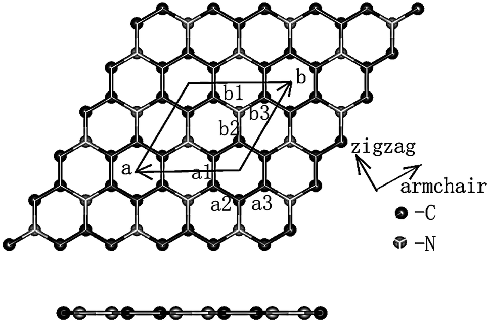 | ||
| Fig. 1 Top view and side view optimized atomic configuration of monolayer C3N. (a1)–(a3) is the bond length between C and C atoms in different position. (b1)–(b3) is the bond length between C and N atoms in different position. | ||
Monolayer C3N belongs to the space group P6/mmm. The lattice parameter for it is a = 4.86 Å. The applied in-layer strain in our study is defined as ε% = (a − a0)/a0, where a is the lattice constants of the strained structure and a0 is the lattice constants of strain free structure. The strain within the suitable range from −10% compressive strain to 10% tensile strain was applied in either uniaxial or biaxial direction to explore its effects on the electronic and optical properties. Because the structure of C3N exhibits a high symmetry, the uniaxial strain along the a lattice vector direction could be regarded as equivalent to the uniaxial strain along the b lattice vector direction. So the uniaxial strain we adopted in this paper is the uniaxial strain along the direction of the lattice vector a. With each uniaxial or biaxial strain applied, the structure was fully relaxed.
When first-principles calculations are used to measure optical properties, the results are varied when different methods are being used. Each method has its own advantages and disadvantages.42 H–F based methods are the most efficient one among the three methods, but the spectrum higher energy peaks are missing.42 TDDFT is less efficient compared with H–F based methods, and the spectrum can be obtained in both visible and ultraviolet region.42 However, some of the low energy peaks in the spectrum region are missing.42 As for perturbation theory method, it is not as efficient as the first two methods mentioned above and requires more time and calculated resources. However, it could be more accurate in whole energy regions.42 Therefore, in calculation of the optical properties in this paper, perturbation theory method was used based on VASP code. The relevant parameters such as reflectivity R(ω), refractive index N(ω), absorption coefficient I(ω) were obtained from the results of dynamical dielectric response functions ε(ω). The computational formulas between ε(ω) and the relevant optical parameters were as follows:
| ε(ω) = ε1(ω) + iε2(ω), | (1) |
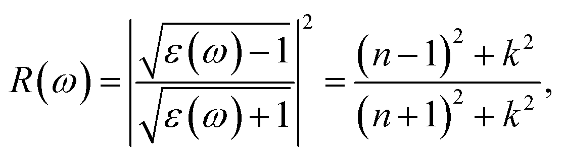 | (2) |
| N(ω) = n(ω) + ik(ω), | (3) |
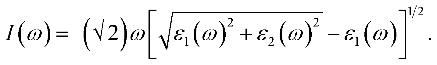 | (4) |
3 Results
3.1 Strain effect on the structural properties of monolayer C3N
To deeply study the uniaxial strain and biaxial strain effect on the optical properties and electronic properties of monolayer C3N, the structural properties of monolayer C3N must be firstly addressed. Fig. 1 exhibits the structure of monolayer C3N. Monolayer C3N belongs to the space group P6/mmm. The lattice parameters for it are a0 = b0 = 4.86 Å. In this study, the structure of monolayer C3N we built is composed of a number of hexagonal C rings with N atomics connecting them, which is the same as the structure in the existing experiment of monolayer C3N.37 After fully relaxed the monolayer structure of C3N, all atoms tend to be remain in one flat sheet, just like graphene. The optimized structural parameters are list in Table 1.To confirm the stability of monolayer C3N, we examined the phonon spectra of monolayer C3N by using linear response method based on CASTEP package and found no imaginary phonon modes over the entire Brillouin zone (BZ) (Fig. 2), indicating the structure of monolayer C3N is dynamically stable. This result consists well with the previous study.41 Further more, the optimized values of lattice constant, total energy of system (Etot), bond length between C and C (dC–C), bond length between C and N (dC–N) and the band gap (Egap) of strain free monolayer C3N are given in Table 1. Combined with Fig. 1 and Table 1, we can see that the monolayer C3N exhibits high geometric symmetry along the directions of a lattice vector and b lattice vector.
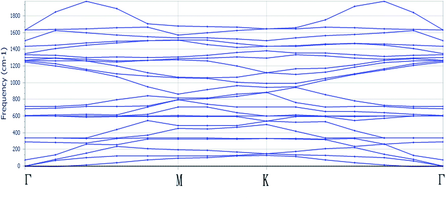 | ||
| Fig. 2 The phonon dispersion spectrum for monolayer C3N. | ||
We next turn to discuss the in-layer strain effect on the change of structural properties (Fig. 3). Firstly, the strain energy, which defined as the difference in the energy between the strained C3N and the strain free C3N,47 of system increases with both increasing the compressive strain (from 0% to −10%) and tensile strain (from 0% to 10%). As we can see, the minimum strain energy is located at ε = 0%, that is to say, the most stable structure of monolayer C3N is the strain free structure. Secondly, the optimized lattice constant a and b of monolayer C3N increases linearly with altering the biaxial strain from ε = −10% to ε = 10%. And lattice constant a is equal to b throughout the process when altering the biaxial strain from ε = −10% to ε = 10%. However, when we applied uniaxial strain along a lattice vector, the optimized lattice constant a and b of monolayer C3N increases nonlinearly by altering the uniaxial strain from ε = −10% to ε = 10%. What's more, by changing the uniaxial strain, the change of lattice constant a is much larger than that of lattice constant b which indicated that monolayer C3N has anisotropic property when applying uniaxial strain. Thirdly, the bond length of monolayer C3N is increasing continuously with altering strain from −10% to 10%, however, when biaxial strain is applied, all C–C bond lengths are the same and all C–N bond lengths are the same. When uniaxial strain is applied, the lengths of C–C bond and C–N bond at different positions are different, and their variations are different. As we can see, the structural property of monolayer C3N reveals isotropy when biaxial strain is applied, and anisotropy when uniaxial strain is applied.
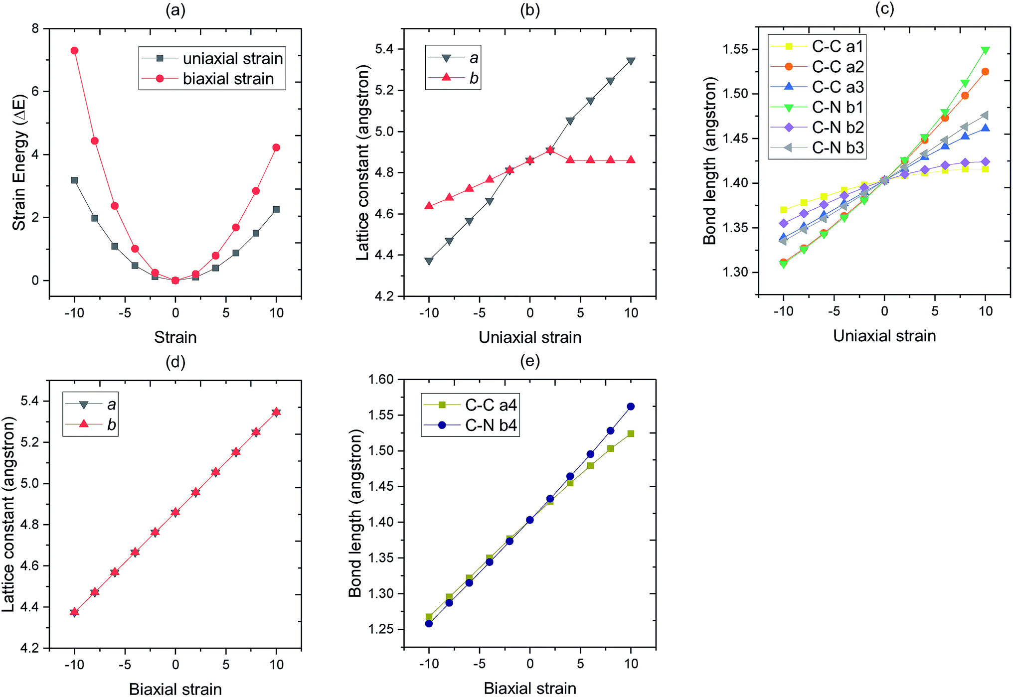 | ||
| Fig. 3 Basic optimized properties of C3N monolayer in different strain (from −10% to 10%). Panel (a) displays the strain energy of C3N system by applying uniaxial strain (black) and biaxial strain (red) reflectivity. In panel (b), different points represent the lattice constant of C3N under different uniaxial strain respectively. In panel (c) the different point represent the bond length of C–C and C–N when uniaxial strain applied, respectively. In panel (d), different points represent the lattice constant of C3N under different biaxial strain respectively. In panel (e) the different point represent the bond length of C–C and C–N when biaxial strain applied, respectively. | ||
3.2 Strain effect on the electronic properties of monolayer C3N
In terms of electronic properties, first of all, we explored the electronic properties of strain free monolayer C3N. The band structure and density of states of strain free monolayer C3N are calculated by PBE method. What's more, the HSE06 method is utilized to revise the band gap (Fig. 4). We can see that monolayer C3N exhibit semiconductivity with an indirect band gap which corresponding band gaps are 0.39 eV by using PBE method and 0.94 eV by using HSE06 method when the strain is 0%. The stable semiconductive character of C3N in our study has also been proved in the experiment.37 Our results of the band gap are good agreement with the previous theoretical results.32–35 We compared the experimental and theoretical results of band gap as shown in Table 2. The valence band maximum (VBM) of monolayer C3N is located at M point and the conduction band minimum (CBM) is located at Γ point when strain is 0% (Fig. 4(a) and (b)). According to the analysis of the PDOS of strain free monolayer C3N, as showed in Fig. 4(c1)–(d3), the VBM and CBM are occupied by py orbital of both N and C atoms.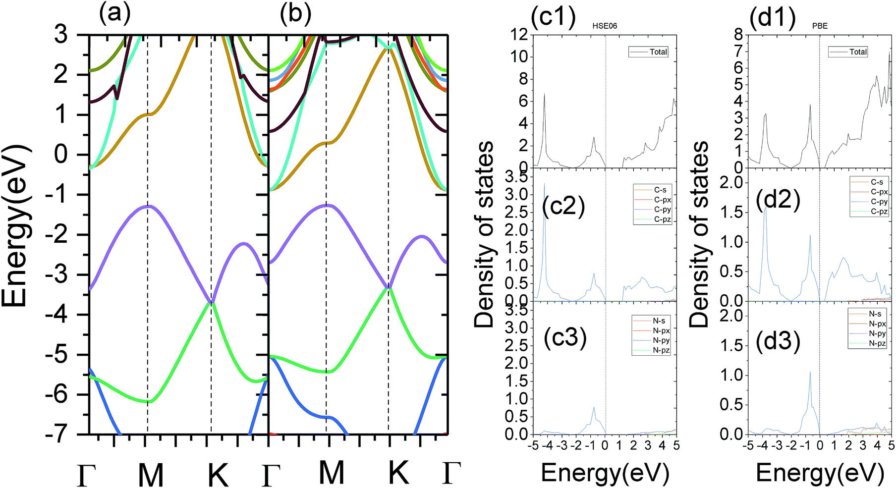 | ||
| Fig. 4 Calculated electronic properties of strain free monolayer C3N. (a) and (b) show the band structure of strain free C3N by using HSE06 method and PBE method respectively. (c1)–(c3) display the electronic density of states of strain free C3N by using HSE06 method. (d1)–(d3) display the electronic density of states of strain free C3N by using PBE method. | ||
Furthermore, due to the carrier transport has close relationship with the properties of different frontier states, we next discuss the character of frontier states in strain free monolayer C3N.
Fig. 5(a) and (b) display the electron partial charge density of VBM mainly derives from C and N atoms. The partial charge density of CBM mainly induced by C atoms, while a small part comes from N atom. This result consists well with the result of the analysis of PDOS (Fig. 5).
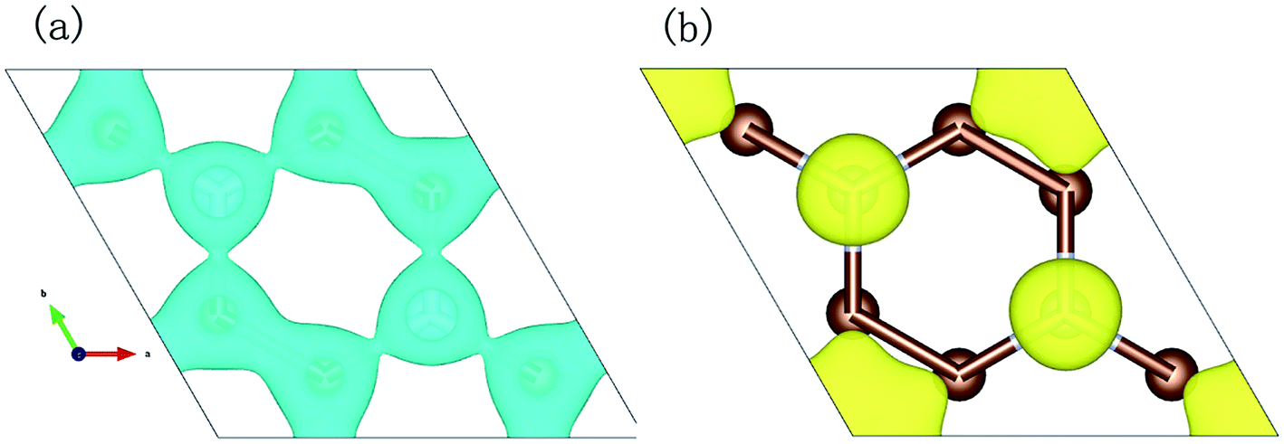 | ||
| Fig. 5 The charge density for monolayer C3N respectively. (a) Shows the top view of charge density for VBM of monolayer C3N. (b) Shows the top view of charge density for CBM of monolayer C3N. | ||
Then we consider the changes of electronic properties of monolayer C3N by applying biaxial strain and uniaxial strain. Fig. 6 illustrates the calculated band gap of monolayer C3N as a function of biaxial strain applied (a) and uniaxial strain applied (b) by using PBE and HSE06 methods, respectively. With regard to this figure, the band gap of monolayer C3N basically keeps increasing with the either biaxial strain or uniaxial strain changes from −6% compressive strain to 10% tensile strain. The most striking distinction between the PBE method and the HSE06 method is that when the compressive strain is greater than −8%, the band gap becomes zero when the PBE method is used, while the band gap does not come to zero when the HSE06 method is used. The main reason for this difference is that the PBE method underestimates the band gap, while the HSE06 method could further revise the band gap. Based on the HSE06 calculation, monolayer C3N could maintain indirect semiconductive characters under different biaxial and uniaxial strain from ε = −10% to ε = 10%.
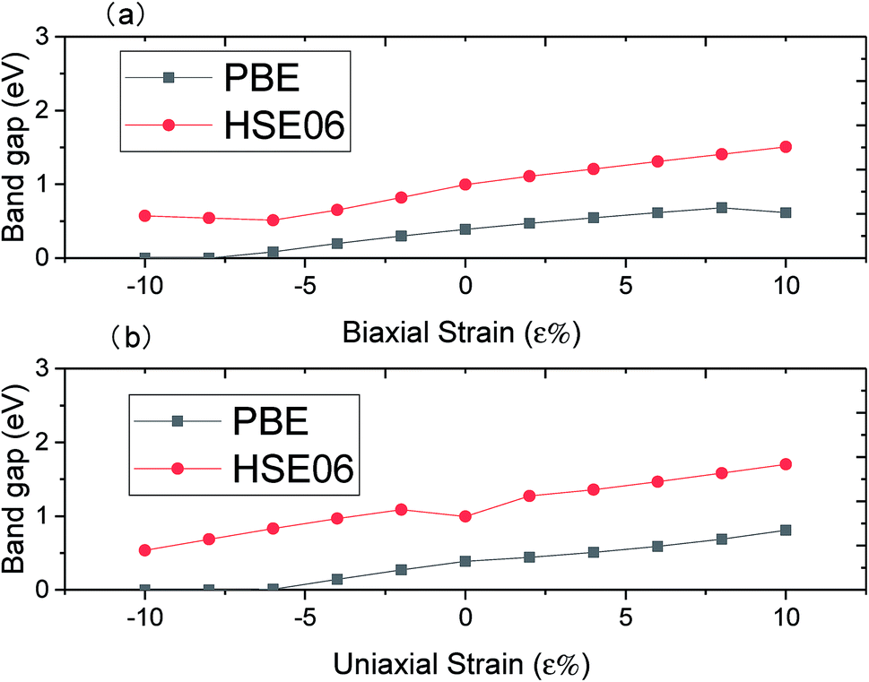 | ||
| Fig. 6 Panel (a) and (b) show the band gap of monolayer C3N when applying biaxial strain and uniaxial strain (from −10% to 10%) by PBE method and HSE06 method, respectively. | ||
Above results reveal that monolayer C3N exhibits semiconductivity with an moderate indirect band gap, and it can maintain this semiconductor character when biaxial or uniaxial strain applied in the range from ε = −10% to ε = 10%. In addition the band gap of monolayer C3N could be tuned easily via strain and the changes of electronic properties of monolayer C3N by applying uniaxial strain and biaxial strain are different. All these results indicate that monolayer C3N should be suitable for the applications in nanoelectronics.
3.3 Strain effect on the optical properties of monolayer C3N
Above calculations reveal that monolayer C3N shows high stability and suitable band gap, turning it into a promising optoelectronic application. In terms of the calculations of optical properties, we also use PBE method to study its optical properties, and the HSE06 method is used to further modify the absorption edge and reflective coefficient. The primary task of optical calculation is solving the imaginary part and real part of the frequency dependent dielectric function ε(ω).In our calculation, the frequency dependent imaginary part of the dielectric function is defined as follow:
 | (5) |
In this equation, c and v refer to conduction and valence band states respectively, and uck is the cell periodic part of the wavefunctions at the k-point k. In addition, the real part of the dielectric function is obtained by the eqn (6) as follow.
 | (6) |
In eqn (6), index P denotes the principle value.31 By computing the dielectric function, the absorption and reflectivity spectra of monolayer C3N can be obtained by using eqn (1)–(5).
Firstly, we consider the optical properties of strain free monolayer C3N. We can get similar results of optical properties by using both PBE and HSE06 methods. The main differences in the results between the two methods lie in the differences of optical absorption edges, static dielectric constants, reflective coefficient and the peak value of each curve.
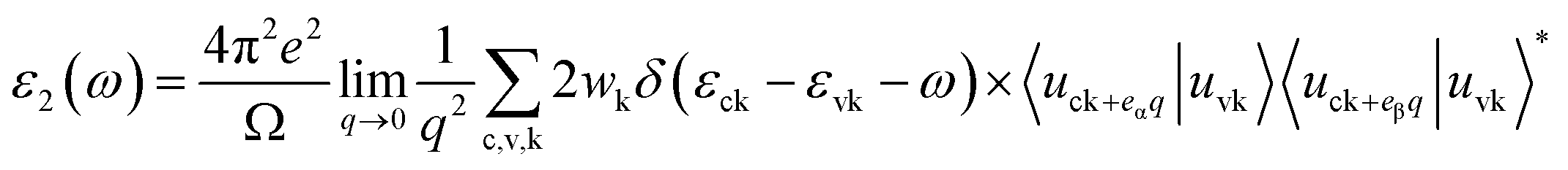
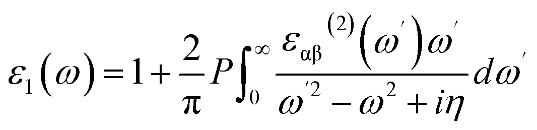
The results are as follows: firstly, we studied the optical absorption properties of monolayer C3N by analyzing the imaginary part of dielectric function diagram and the optical absorption coefficient spectra (Fig. 7 and 8). Results obtained by PBE method indicate the optical absorption edge of monolayer C3N is 0.7 eV and the first absorption peak at 2.24 eV (Fig. 7). When the HSE06 method was used, photons were absorbed by strain free monolayer C3N start to absorb photons nearly in 1.5 eV, and the first absorption peak is around 3.1 eV (Fig. 8). What's more, the absorption spectrum shows that the main absorption region of strain free monolayer C3N includes basically all visible light areas (1.6–3.1 eV) by using both PBE method and HSE06 method. Secondly, we studied the optical reflectivity properties of monolayer C3N by analyzing the real part of dielectric function diagram and the optical reflectivity spectra (Fig. 7 and 8). The results exhibit the static dielectric constant and static reflectivity of monolayer C3N are 2.96 and 0.07 by using PBE method (Fig. 7) and 1.9 and 0.025 by using HSE06 method (Fig. 8).
 | ||
| Fig. 7 Optical spectra of monolayer C3N by using PBE method. 4 panels indicate the calculated values of imaginary part of dielectric function ε2, real part of dielectric function ε1, optical reflectivity coefficient R and optical absorption coefficient I, respectively. | ||
 | ||
| Fig. 8 Optical spectra of monolayer C3N by using HSE06 method. 4 panels indicate the calculated values of imaginary part of dielectric function ε2, real part of dielectric function ε1, optical reflectivity coefficient R and optical absorption coefficient I, respectively. | ||
Our results reveal that strain free monolayer C3N display the same exciton effect along the armchair and zigzag directions which mean the optical absorption property of strain free monolayer C3N are isotropic along the armchair and zigzag directions.
When in-layer strain is applied, the variations of optical properties of monolayer C3N are as follows. Fig. 9(c1) and 10(c1) show the effects of biaxial strain on the optical absorption properties of monolayer C3N obtained by PBE method and HSE06 method respectively. We can see that, firstly, the absorption edge almost remains unchanged when the biaxial strain alters from ε = −10% to ε = 10%. Secondly, the major characteristic peaks of optical absorption vary significantly. Particularly, the first absorption peak decreases when changing the biaxial strain from ε = 0% to ε = 10% and increases when changing the biaxial strain from ε = 0% to ε = −10%. The first absorption peak exhibits a red-shift from ε = −10% to ε = 10%. What's more, when biaxial tensile strain is applied, a new absorption peak appears in the deep ultraviolet region near 12 eV. When altering the biaxial strain from ε = 0% to ε = 10%, this new peak increases and exhibits a red-shift. Thirdly, the variations of optical reflectivity properties of monolayer C3N with changing the biaxial strain are analyzed from the optical reflectivity coefficient spectras (Fig. 9(c2) and 10(c2)). The static reflectivity of monolayer C3N shows a increasing trend from ε = 0% to ε = −10% and a decreasing trend from ε = 0% to ε = 10%.
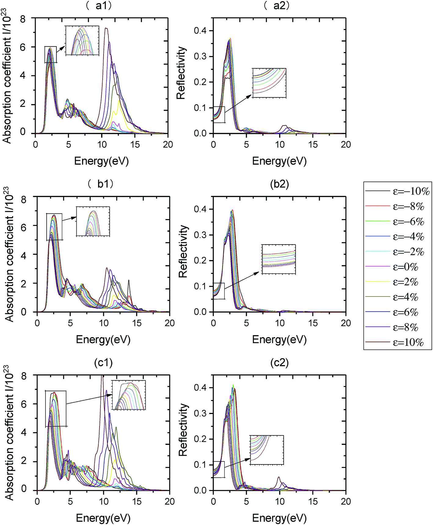 | ||
| Fig. 9 Optical spectra of monolayer C3N by applying different uniaxial strain and biaxial strain obtained by PBE method. Panels (a1) and (b1) represent the optical absorption coefficient I of monolayer C3N along the armchair direction and zigzag direction when uniaxial strain applied, respectively. Panels (a2) and (b2) represent the optical reflectivity coefficient R of monolayer C3N along the zigzag direction when uniaxial strain applied, respectively. Panels (c1) and (c2) exhibit the variations of optical absorption coefficient I and optical reflectivity coefficient R of monolayer C3N when biaxial strain applied, respectively. | ||
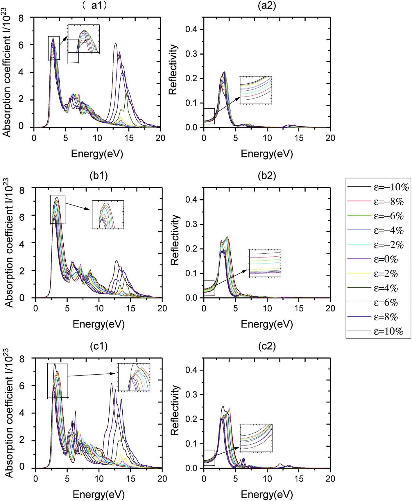 | ||
| Fig. 10 Optical spectra of monolayer C3N by applying different uniaxial strain and biaxial strain obtained by HSE06 method. Panels (a1) and (b1) represent the optical absorption coefficient I of monolayer C3N along the armchair direction and zigzag direction when uniaxial strain applied, respectively. Panels (a2) and (b2) represent the optical reflectivity coefficient R of monolayer C3N along the zigzag direction when uniaxial strain applied, respectively. Panels (c1) and (c2) exhibit the variations of optical absorption coefficient I and optical reflectivity coefficient R of monolayer C3N when biaxial strain applied, respectively. | ||
Fig. 9(a1), (b1), 10 (a1) and (b1) show the effects of uniaxial strain on the optical absorption properties of monolayer C3N obtained by PBE method and HSE06 method respectively. We find that, the absorption properties along armchair and zigzag directions exhibit anisotropic property when we applied uniaxial strain.
For armchair direction, firstly, the absorption edge almost remains unchanged when the uniaxial strain alters from ε = −10% to ε = 10%. Secondly, the first absorption peak decreases when changing the biaxial strain from ε = 0% to ε = ±10%. The first absorption peak exhibits a blue-shift from ε = 0% to ε = −10% and a red-shift from ε = 0% to ε = 10%. What's more, when uniaxial tensile strain is applied, a new absorption peak appears in the deep ultraviolet region near 12 eV. When altering the uniaxial strain from ε = 0% to ε = 10%, this new peak increases and exhibits a red-shift. Fig. 9(a1) and 10(a1) Thirdly, the variations of optical reflectivity properties of monolayer C3N with changing the uniaxial strain are analyzed from the optical reflectivity coefficient spectras (Fig. 9(a2) and 10(a2)). The static reflectivity of monolayer C3N shows a increasing trend from ε = 0% to ε = 10% and a decreasing trend from ε = 0% to ε = −10%.
For zigzag direction, firstly, the absorption edge almost remains unchanged when the biaxial strain alters from ε = −10% to ε = 10%. Secondly, the first absorption peak decreases when changing the uniaxial strain from ε = 0% to ε = 10% and increases when changing the uniaxial strain from ε = 0% to ε = −10%. The first absorption peak exhibits a red-shift from ε = −10% to ε = 10%. What's more, when uniaxial tensile strain is applied, a new absorption peak appears in the deep ultraviolet region near 12 eV. The value of this peak along zigzag direction is much lower than it along armchair direction, when altering the uniaxial strain from ε = 0% to ε = 10%, this new peak increases and exhibits a red-shift. When altering the uniaxial strain from ε = 0% to ε = −10%, this new peak decreases and exhibits a blue-shift (Fig. 9(b1) and 10(b1)). Thirdly, the variations of optical reflectivity properties of monolayer C3N with changing the uniaxial strain are analyzed from the optical reflectivity coefficient spectras (Fig. 9(b2) and 10(b2)). The static reflectivity of monolayer C3N increases from ε = 0% to ε = −10% and decreases from ε = 0% to ε = 10%.
Above results indicates that the absorption and reflectivity properties along armchair and zigzag directions exhibit anisotropic property when we applied uniaxial strain. However, when we applied biaxial strain, the absorption and reflectivity properties along armchair and zigzag directions show isotropic property. Moreover, uniaxial tensile strain and biaxial tensile strain could cause the high absorption coefficient of monolayer C3N in the deep ultraviolet region.
Combined with the results of the structural property, we suggest that, when biaxial strain is applied, the isotropic structural property induced the isotropic optical property of monolayer C3N. However, when uniaxial strain is applied, the completely different response of C–C and C–N chemical bond in different positions caused the anisotropic structural property which induced the anisotropic optical property of monolayer C3N.
We have calculated the electron density distribution in the corresponding energy range of the valence electron under different strains and made a figure of it based on the result (Fig. 11). From the calculated results, we found that when uniaxial tensile strain is applied, the appearance of the new absorption peak in the deep ultraviolet region near 12 eV when uniaxial tensile strain is applied is because of the electronic transitions between N pz orbitals to conductive band.
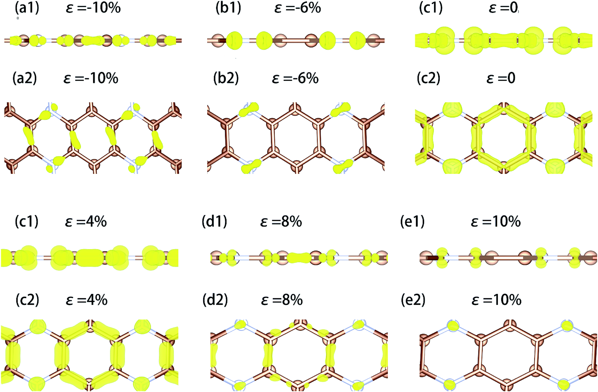 | ||
| Fig. 11 The electron density distribution of monolayer C3N when uniaxial strain applied, respectively. The isosurface is set to 0.0103. (a1)–(e1) is the side view and (a2)–(e2) is the top view. Brown atom is the C atom and the white atom is the N atom. | ||
It can be seen that the optical properties of monolayer C3N are the same as those of two-dimensional materials such as black phosphene45 and BC3,44 which can be effectively tuned by the applied strain. However, the optical properties of these 2D monolayer materials have their own characteristics when the applied strain changes. For example, when the strain changes from compressive strain to tensile strain, the absorption edge of BC3 displays a blue shift and the static reflectivity coefficient decreases, while the absorption edge of black phosphene shows a red shift and the peak value of absorption coefficient decreases. Especially, 2D C3N exhibits a unique characteristic when tensile strain is applied. It produces an obvious absorption peak in the deep ultraviolet region.
In addition, the optical anisotropy of black phosphene has been studied experimentally by Wang et al.46 The optical properties obtained from the Raman spectra and photoluminescence spectra in their work are in good agreement with first-principles calculations. Their work not only provides experimental guidance for the practical synthesis of 2D materials and the rational application of their optical properties but also proves the correctness of theoretical research for 2D materials. Encouraged by their work, we hope that monolayer C3N would be a promising candidate for the strain tunable optoelectronic materials in the future.
4 Conclusions
We have systematically presented a first-principles investigation of the electronic and optical properties of a new two-dimensional (2D) monolayer C3N under different strains. The PBE method is used to calculate the electronic and optical properties, and the hybrid functional HSE06 method is used to further modify the band gap and optical absorption edge. Based on the HSE06 calculation, monolayer C3N could maintain an indirect semiconductive character under different biaxial and uniaxial strain from ε = −10% to ε = 10%. In terms of the optical property, first of all, we have found that both uniaxial tensile strain and biaxial tensile strain can lead to a high absorption coefficient of monolayer C3N in a deep UV region. Moreover, an anisotropic optical property is presented when uniaxial strain is applied, while an isotropic optical property is shown when we applied biaxial strain. Therefore, strain engineering can be an effective approach to change the electronic and optical properties of monolayer C3N. Based on our study, we believe that monolayer C3N is a promising candidate in the applications of optoelectronics and nanoelectronics.Author contributions
Qing-Yuan Chen carried out the DFT calculations and prepared the manuscript. M. Y. L., C. C. and Y. H. Contributed the discussion and suggestions. All authors read the manuscript.Conflicts of interest
The authors declare no competing financial interests.Acknowledgements
This work was supported by National Natural Science Foundation of China (Grant No. U1502272 and 61751405), Precious Metal Materials Genetic Engineering Major Project of Yunnan Province (Grant No. 2018ZE006, 2018ZE023 and 2018IC058), Program of High-end Scientific and Technological Talents in Yunnan Province (Grant No. 2013HA019), Program for Yunling Scholars in Yunnan Province, Program for Donglu Scholars in Yunnan University, New Academic Researcher Award for Doctoral Candidates of Yunnan Province. Computational resources were provided by the High Performance Computing Center of Yunnan University.References
- H. Guo, N. lu, L. Wang, X. Wu and X. C. Zeng, Tuning Electronic and Magnetic properties of early transition-metal dichalcogenides via Tensile strain, J. Phys. Chem. C, 2014, 118, 7241–7249 Search PubMed.
- K. S. Novoselov, A. K. Geim, S. V. Morozov, D. Jiang, Y. Zhang, S. V. Dubonos, L. V. Grigorieva and A. A. Firsov, Electric Field Effect on Atomically Thin Carbon Films, Science, 2004, 306, 666–669 CrossRef CAS PubMed.
- N. Lu, Z. Li and J. Yang, Electronic Structure Engineering via On Plane Chemical Functionalization: A Comparison Study on Two Dimensional Polysilane and Graphene, J. Phys. Chem. C, 2009, 113, 16741–16746 CrossRef CAS.
- H. Guo, Y. Zhao, N. Lu, E. Kan, X. C. Zeng, X. Wu and J. Yang, Tunable Magnetism in a Nonmetal-Substituted ZnO Monolayer: A First-Principles Study, J. Phys. Chem. C, 2012, 116, 11336–11342 CrossRef CAS.
- J. Dai, X. Wu, J. Yang and X. C. Zeng, Unusual Metallic Microporous Boron Nitride Networks, J. Phys. Chem. Lett., 2013, 4, 3484–3488 CrossRef CAS.
- H. Liu, A. T. Neal, Z. Zhu, Z. Luo, X. Xu, D. Tománek and P. D. Ye, Phosphorene: an unexplored 2D semiconductor with a high hole mobility, ACS Nano, 2014, 8, 4033–4041 CrossRef CAS PubMed.
- L. Li, Y. Yu, G. J. Ye, Q. Ge, X. Ou, H. Wu, D. Feng, X. H. Chen and Y. Zhang, Black phosphorus field-effect transistors, Nat. Nanotechnol., 2014, 9, 372 CrossRef CAS PubMed.
- C. Si, Z. Liu, W. Duan and F. Liu, First-principles calculations on the effect of doping and biaxial tensile strain on electron-phonon coupling in graphene, Phys. Rev. Lett., 2013, 111, 196802 CrossRef PubMed.
- X. Chen, Y. Liu, B.-L. Gu, W. Duan and F. Liu, Giant room- temperature spin caloritronics in spin-semiconducting graphene nanoribbons, Phys. Rev. B: Condens. Matter Mater. Phys., 2014, 90, 121403 CrossRef.
- Q. Ke, C. Tang, Y. Liu, H. Liu and J. Wang, Intercalating graphene with clusters of Fe3O4 nanocrystals for electrochemical super- capacitors, Mater. Res. Express, 2014, 1, 025015 CrossRef.
- Q. Ke, Y. Liu, H. Liu, Y. Zhang, Y. Hu and J. Wang, Surfactant- modified chemically reduced graphene oxide for electro-chemical supercapacitors, RSC Adv., 2014, 4, 26398–26406 RSC.
- S. Bertolazzi, D. Krasnozhon and A. Kis, Nonvolatile memory cells based on MoS2/graphene heterostructures, ACS Nano, 2013, 7(4), 3246–3252 CrossRef CAS PubMed.
- E. Zhang, W. Wang, C. Zhang, Y. Jin, G. Zhu, Q. Sun, D. W. Zhang, P. Zhou and F. Xiu, Tunable charge-trap memory based on few-layer MoS2, ACS Nano, 2014, 9(1), 612–619 CrossRef PubMed.
- C. O. H. Hugh and J. H. Pablo, Two-dimensional crystals: phosphorus joins the family, Nat. Nanotechnol., 2014, 9, 330–331 CrossRef PubMed.
- A. Brown and S. Rundqvist, Refinement of the crystal structure of black phosphorus, Acta Crystallogr., 1965, 19, 684 CrossRef CAS.
- S. Zhao, W. Kang and J. Xue, The potential application of phosphorene as an anode material in Li-ion batteries, J. Mater. Chem. A, 2014, 2, 19046–19052 RSC.
- J. Guan, Z. Zhu and D. Tománek, Phase coexistence and metal-insulator transition in few-layer phosphorene: a computational study, Phys. Rev. Lett., 2014, 113, 046804 CrossRef PubMed.
- J. Mahmood, E. K. Lee, M. Jung, D. Shin, H. J. Choi, J. M. Seo, S. M. Jung, D. Kim, F. Li and M. S. Lah, et al., Two-Dimensional Polyaniline (C3N) from Carbonized Organic Single Crystals in Solid State, Proc. Natl. Acad. Sci. U. S. A., 2016, 113, 7414–7419 CrossRef CAS PubMed.
- J. D. Wood, S. A. Wells, D. Jariwala, K.-S. Chen, E. Cho, V. K. Sangwan, X. Liu, L. J. Lauhon, T. J. Marks and M. C. Hersam, Effective passivation of exfoliated black phosphorus transistors against ambient degradatio, Nano Lett., 2014, 14, 6964 CrossRef CAS PubMed.
- J.-S. Kim, Y. Liu, W. Zhu, S. Kim, D. Wu, L. Tao, A. Dodabalapur, K. Lai and D. Akinwande, Toward air-stable multilayer phosphorene thin-films and transistors, Sci. Rep., 2015, 5, 89 Search PubMed.
- N. V. Blinova, J. Stejskal, M. Trchova, G. Ciric-Marjanovic and I. Sapurina, Polymerization of Aniline on Polyaniline Membranes, J. Phys. Chem. B, 2007, 111, 2440–2448 CrossRef CAS PubMed.
- M. Y. Chang, C. S. Wu, Y. F. Chen, B. Z. Hsieh, W. Y. Huang, K. S. Ho, T. H. Hsieh and Y. K. Han, Polymer Solar Cells Incorporating One-Dimensional Polyaniline Nanotubes, Org. Electron., 2008, 9, 1136–1139 CrossRef CAS.
- M. M. Alam, J. Wang, Y. Guo, S. P. Lee and H. R. Tseng, Electrolyte-Gated Transistors Based on Conducting Polymer Nanowire Junction Arrays, J. Phys. Chem. B, 2005, 109, 12777–12784 CrossRef CAS PubMed.
- G. Ciric-Marjanovic, Recent Advances in Polyaniline Research: Polymerization Mechanisms, Structural Aspects, Properties and Applications, Synth. Met., 2013, 177, 1–47 CrossRef CAS.
- H. J. Xiang, B. Huang, Z. Y. Li, S. H. Wei, J. L. Yang and X. G. Gong, Ordered Semiconducting Nitrogen-Graphene Alloys, Phys. Rev. X, 2012, 2, 011003 Search PubMed.
- P. E. Blochl, Projector augmented-wave method, Phys. Rev. B: Condens. Matter Mater. Phys., 1994, 50, 17953 CrossRef.
- G. Kresse and D. Joubert, From ultrasoft pseudopotentials to the projector augmented-wave method, Phys. Rev. B: Condens. Matter Mater. Phys., 1999, 59, 1758 CrossRef CAS.
- O. Leenaerts, B. Partoens and F. M. Peeters, Adsorption of H2O, NH3, CO, NO2, and NO on graphene: a first-principles study, Phys. Rev. B: Condens. Matter Mater. Phys., 2008, 77, 125416 CrossRef.
- L. Chen, L. Wang, Z. Shuai and D. Beljonne, Energy level alignment and charge carrier mobility in noncovalently functionalized graphene, J. Phys. Chem. Lett., 2013, 4, 2158–2165 CrossRef CAS.
- J. Heyd, G. E. Scuseria and M. Ernzerhof, Hybrid functionals based on a screened Coulomb potential, J. Chem. Phys., 2003, 118, 8207–8215 CrossRef CAS.
- X. Peng, A. Copple and Q. Wei, Strain-engineered direct-indirect band gap transition and its mechanism in two-dimensional phosphorene, Phys. Rev. B: Condens. Matter Mater. Phys., 2014, 90, 085402 CrossRef.
- C. Zhang, Y. Jiao, T. He, S. Bottle, T. Frauenheim and A. Du, Predicting Two-Dimensional C3B/C3N van der Waals p−n Heterojunction with Strong Interlayer Electron Coupling and Enhanced Photocurrent, J. Phys. Chem. Lett., 2018, 9, 858–886 CrossRef CAS PubMed.
- Y. Qie, J. Liu, S. Wang, S. Gong and Q. Sun, C3B monolayer as an anchoring material for lithium-sulfur batteries, Carbon, 2018, 129, 38–44 CrossRef CAS.
- L. Shi, Y. Zhang, X. Xiu and H. Dong, Structural characteristics and strain behavior of two-dimensional C3N : first principles calculations, Carbon, 2018, 134, 103–111 CrossRef CAS.
- X. Zhou, W. Feng, S. Guan, B. Fu, W. Su and Y. Yao, Computational characterization of monolayer C3N: a two-dimensional nitrogen-graphene crystal, J. Mater. Res., 2017, 32, 15 Search PubMed.
- L. Xie, L. Yang, W. Ge, X. Wang and J. Jiang, Bandgap tuning of C3N monolayer: a first-principles study, Chem. Phys., 2019, 520, 40–46 CrossRef CAS.
- J. Mahmood, E. K. Lee, M. Jung, D. Shin, H. J. Choi, J. M. Seo, S. M. Jung, D. Kim, F. Li, M. S. Lah, N. Park, H. J. Shin, J. H. Oh and J. B. Baek, Two-dimensional polyaniline (C3N) from carbonized organic single crystals in solid state, Proc. Natl. Acad. Sci. U. S. A., 2016, 113, 7414–7419 CrossRef CAS PubMed.
- M. Makaremi, B. Mortazavi and C. V. Singh, Adsorption of Metallic, Metalloidic, and Nonmetallic Adatoms on Two-Dimensional C3N, J. Phys. Chem. C, 2017, 121, 18575–18583 CrossRef CAS.
- X. Zhou, W. Feng, S. Guan, B. Fu, W. Su and Y. Yao, Computational characterization of monolayer C3N: a two-dimensional nitrogen-graphene crystal, J. Mater. Res., 2017, 32, 2993–3001 CrossRef CAS.
- C. Zhang, Y. Jiao, T. He, S. Bottle, T. Frauenheim and A. Du, Predicting Two-Dimensional C3B/C3N van der Waals p–n Heterojunction with Strong Interlayer Electron Coupling and Enhanced Photocurrent, J. Phys. Chem. Lett., 2018, 9, 858–862 CrossRef CAS PubMed.
- X. Wang and J. Chen, Phonon-mediated superconductivity in charge doped and Li-deposited two dimensional C3N, Phys. C, 2019, 558, 12–16 CrossRef CAS.
- R. K. Shivade and B. Chakraborty, Optical absorption spectra of boron clusters Bn (n = 2–5) for application in nano scintillator – a time dependent density functional theory study, Eur. Phys. J. B, 2016, 89, 198 CrossRef.
- S. Kumar, S. Sharma, V. Babar and U. Schwingenschlögl, Ultralow lattice thermal conductivity in monolayer C3N as compared to graphene, J. Mater. Chem. A, 2017, 5, 20407–20411 RSC.
- Y. Zhang, Z.-F. Wu, P.-F. Gao, D.-Q. Fang, E.-H. Zhang and S.-L. Zhang, Strain-tunable electronic and optical properties of BC3 monolayer, RSC Adv., 2018, 8, 1686–1692 RSC.
- Z. Xie, L. Hui, J. Wang, G. A. Zhu, Z. Chen and C. Li, Electronic and optical properties of monolayer black phosphorus induced by bi-axial strain, Comput. Mater. Sci., 2018, 144, 304–314 CrossRef CAS.
- X. Wang, A. M. Jones, K. L. Seyler, V. Tran, Y. Jia, H. Zhao, H. Wang, L. Yang, X. Xu and F. Xia, Highly anisotropic and robust excitons in monolayer black phosphorus, Nat. Nanotechnol., 2015, 10(6), 517–521 CrossRef CAS PubMed.
- G. Yang, T. Ma and X. Peng, Superior mechanical flexibility and strained-engineered direct-indirect band gap transition of green phosphorene, Appl. Phys. Lett., 2018, 112, 241904 CrossRef.
Footnote |
| † Electronic supplementary information (ESI) available. See DOI: 10.1039/c9ra01024f |
| This journal is © The Royal Society of Chemistry 2019 |