
 Open Access Article
 This Open Access Article is licensed under a Creative Commons Attribution-Non Commercial 3.0 Unported Licence
Tunable gap in stable arsenene nanoribbons opens the door to electronic applications†
A. García-Fuente *a,
J. Carreteb,
A. Vegac and
L. J. Gallegod
*a,
J. Carreteb,
A. Vegac and
L. J. Gallegod
aDepartamento de Física, Universidad de Oviedo, E-33007 Oviedo, Spain. E-mail: garciaamador@uniovi.es
bInstitute of Materials Chemistry, TU Wien, A-1060 Vienna, Austria
cDepartamento de Física Teórica, Atómica y Óptica, Universidad de Valladolid, E-47011 Valladolid, Spain
dDepartamento de Física de la Materia Condensada, Facultad de Física, Universidad de Santiago de Compostela, E-15782 Santiago de Compostela, Spain
First published on 16th April 2019
Abstract
Arsenic has been predicted to present significantly more diverse 2D phases than other elemental compounds like graphene. While practical applications must be based on finite arsenene samples, like nanoribbons, theory has so far focused on the infinite sheet. Our ab initio simulations show the clear contrast between the properties of arsenene nanoribbons and those of the monolayer, ranging from phase stability to electronic structure. We include nanoribbons derived from the buckled, puckered and square/octagon structures of bulk arsenene. The flexibility afforded by different parent structures, widths and edge passivations leads to a rich variety of semiconducting structures with tunable gaps.
1 Introduction
Two-dimensional (2D) materials beyond graphene are attracting growing attention (see, e.g., ref. 1 and references therein). Due to the difficulties of nanoscale experimentation, theory often unveils promising candidates before they can be synthesized and characterized. Silicene and germanene, for instance, were first theoretically investigated in free-standing form,2,3 their existence only later being confirmed by means of substrate-mediated epitaxial growth experiments.4–6Applications of graphene, silicene and germanene2,3,7,8 as channel and emission materials in (on/off) switching and light-emitting devices run up against the problem of their zero band gap. This has spurred research into chemical functionalization9 and related techniques, but also into alternative, semiconducting 2D materials. The successful fabrication of high-performance field-effect transistors using thin flakes of black phosphorene,10 specifically, has attracted attention to group-V candidates. Theoretical studies have shown the stability of black and blue phosphorene with puckered and buckled structures respectively,11,12 and provided an extensive account of the electronic and mechanical properties of nitrogene, arsenene, antimonene and bismuthene (see ref. 13 and references therein) to complement the description of infinite monolayers of group-V 2D materials. Remarkably, those studies show that, with the single exception of nitrogene (a wide-gap insulator), all of them are semiconductors with buckled (b), puckered (p), or square/octagon (s/o) structures, and fundamental band gaps ranging from 3 to 0.15 eV, rendering them potentially suitable for diverse applications in 2D electronics.
Despite these encouraging results, the topic is far from closed. Some of us have recently shown14 that, due to phonon contributions not included in previous studies, the relative stability of the b, p and s/o proposed phases of arsenene13,15,16 is both temperature dependent and clearly at odds with existing predictions. This finding is crucial since accurate determination of the stable geometry of a nanostructure, in general, is a prerequisite to precisely establishing its physico-chemical properties. Similarly, those pioneering studies restricted themselves to the infinite monolayer of each 2D structure, but real devices require specific nanostructures with particular geometries. Although some theoretical studies on arsenene and antimonene nanoribbons in the buckled form have been performed,17 most efforts in this domain have concentrated on phosphorene nanoribbons; for instance, Zhang et al.18 have studied their electronic and transport properties for different widths and edge configurations, predicting them to have very high figures of merit at room temperature. Motivated by the structural diversity of arsenenes, here we report an ab initio density functional theoretic (DFT) study of the structures, stability and electronic properties of arsenene nanoribbons (AsNRs) including both phonons and edge effects. We show that by conceptually cutting the three proposed stable structures of 2D arsenene indicated above (b, p and s/o) along different directions we obtain a large variety of nanostructures with electronic properties of interest. In particular, the band gaps of AsNRs can be tuned within a wide range by selecting the 2D parent structure, the cutting direction, and the ribbon width. Moreover, the relative stability of the b, p, and s/o AsNRs does not simply follow that of the bulk 2D phases. Hence, although only supported, multilayer AsNRs have already been synthesized,19 our results point to the interest of analyzing the potential uses of these nanostructures.
Our calculations were performed using VASP20,21 and the Phonopy package.22 Details of the method can be found in the ESI.†
2 Results and discussion
Our starting point are the geometric and electronic structures of the infinitely extended b, p and s/o arsenene sheets, as obtained by DFT calculations. In ref. 14 some of us performed optimizations of these structures within the Perdew–Burke–Ernzerhof (PBE) form of the GGA,23 and the results are reproduced in ESI Fig. 1.† To complete the information, we now computed their electronic band structures using both PBE and the hybrid functional HSE06.24–27 Our results, shown in ESI Fig. 2,† are in good agreement with those reported by Ciraci and coworkers.13,28 The effect of the HSE correction essentially amounts to a rigid displacement of all bands away from the center of the gap. Therefore the fundamental band gaps are substantially increased, as can be seen in ESI Table 1.†By conceptually cutting nanometer-scale-width strips out of the b, p and s/o arsenene structures along the directions indicated in ESI Fig. 1,† we obtained nanoribbons that share their basic geometries with their 2D precursors and have edges of different shapes. Specifically, we obtained zigzag and armchair buckled arsenene nanoribbons (zz-b-AsNRs and ac-b-AsNRs), zigzag and armchair puckered arsenene nanoribbons (zz-p-AsNRs and ac-p-AsNRs), and “toothy” and armchair square-octagon arsenene nanoribbons (t-s/o-AsNRs and ac-s/o-AsNRs). We considered ribbon widths ranging from 5 to 30 Å, both with free edge atoms and with hydrogen passivation along the edges – a common practice to stabilize nanoribbons. Hydrogen-passivated arsenene nanoribbons will be denoted as H-zz-b-AsNRs and so on and so forth. Fig. 1 shows the relaxed structures of an illustrative sample of AsNRs with similar widths of around 15 Å, and Fig. 2 shows their bond-length distributions. The upper panels of Fig. 3 shows the cohesive energies per atom of all the nanoribbons investigated in this paper. Those are calculated as
 | (1) |
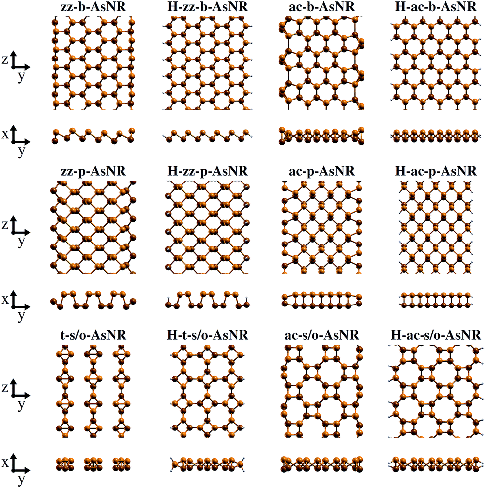 | ||
| Fig. 1 Top and front views of the relaxed structures of illustrative non-passivated and hydrogen-passivated AsNRs. | ||
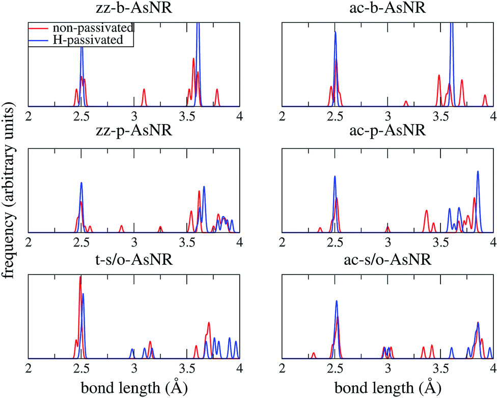 | ||
| Fig. 2 Bond-length distributions of the passivated and non-passivated AsNRs shown in Fig. 1. | ||
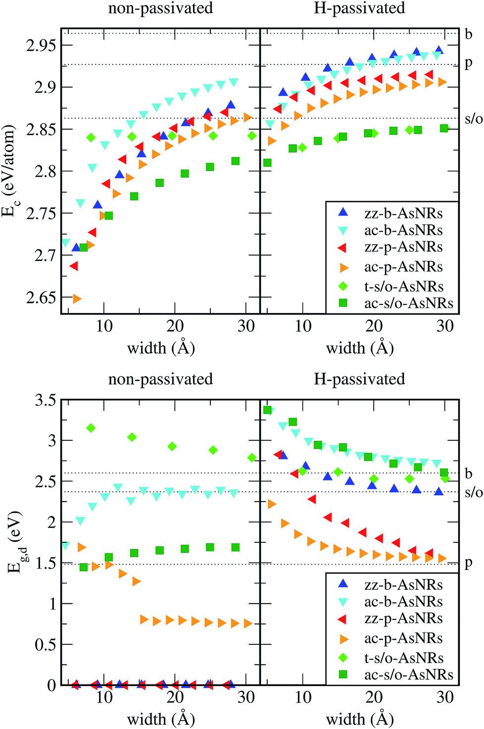 | ||
| Fig. 3 Upper panels: cohesive energies per atom, Ec, of the non-passivated and hydrogen-passivated AsNRs as functions of their widths; the dashed lines correspond to the cohesive energies for the periodic, infinitely extended, p, b and s/o arsenene sheets. Lower panels: direct band gaps of the non-passivated and hydrogen-passivated AsNRs as functions of their widths, calculated with HSE; the dashed lines correspond to the direct band gaps for the periodic, infinitely extended, p, b and s/o arsenene sheets. | ||
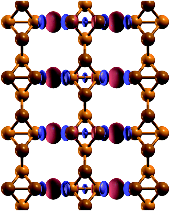 | ||
| Fig. 4 Electronic charge density difference between a t-s/o-AsNR and isolated t-s/o-nanowires. Positive values of the density difference are shown in red, and negative values are shown in blue. | ||
In order to see if the peculiar reconstruction of the t-s/o-AsNRs disappears when the ribbon width is larger than a critical value, we performed calculations on a periodic 2D arrangement of nanowires such as would be obtained if the whole infinite sheet experienced this “lateral dimerization”. The results show that the structure formed by nanowires is also stable in the infinite case, with a cohesive energy of 2.844 eV per atom that is not far from the value we had obtained for the nanoribbons (2.842 eV per atom). Note that the infinite sheet, with 2.86 eV per atom, is more stable also in this case, but both could very well be observed given that the difference is lower than the room-temperature value of kBT, where kB is the Boltzmann constant. Which structure actually appears under specific conditions will depend on the details of the attraction basin of each minimum. In conclusion, no crossover width exists for the phenomenon.
We calculated the band structures of all the AsNRs considered in this paper using both PBE and HSE, and the upper panels of Fig. 5 show the results for the nanoribbons represented in Fig. 1. In the lower panels of Fig. 3 we display the corresponding energy gaps as a function of their widths, obtained using the HSE functional (PBE results are given in the ESI†). Due to the edge reconstruction, the variation of the gap in non-passivated AsNRs is rather irregular. The most striking examples are provided by zz-b-AsNRs and zz-p-AsNRs, which are metallic rather than semiconducting (see Fig. 5, upper panels). The exceptions are, again, the t-s/o-AsNRs, whose particular geometry leads to a regular decrease of the band gap with width. On the other hand, the electronic behavior of the hydrogen-passivated AsNRs is much more regular (upper panels of Fig. 5 and lower right panel of Fig. 3), as a consequence of their general stability. Those nanoribbons are all semiconductors, with band gaps that increase when the widths decrease as a manifestation of confinement effects. The largest band gaps occur for H-ac-s/o-AsNRs and H-ac-b-AsNRs and the smaller ones for H-ac-p-AsNRs. Widths around 30 Å are enough to recover the band gap of the infinite 2D precursors. Additional information on the electronic properties of the AsNRs (specifically, the room temperature carrier densities and mobilities, and the electronic transmittances) is given in the ESI,† corroborating the electronic character already inferred from the energy band structures shown in Fig. 5.
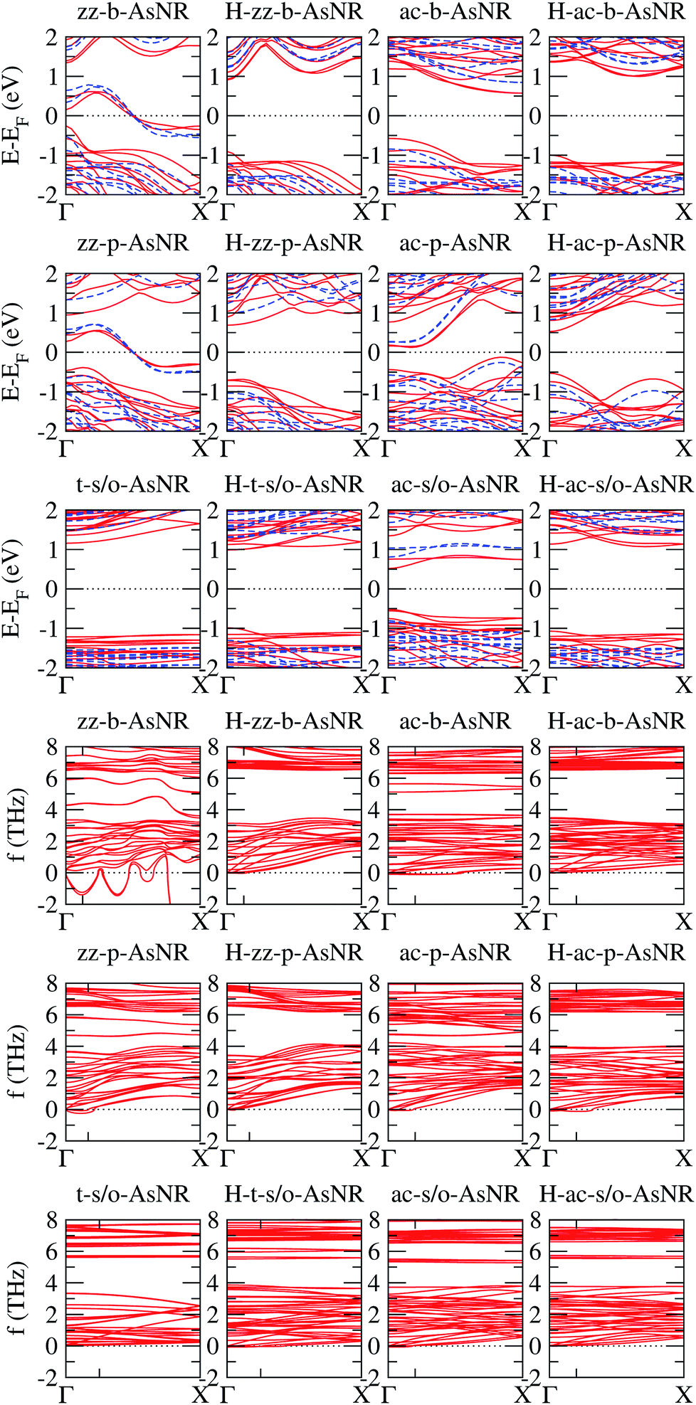 | ||
| Fig. 5 Upper panels: energy band structures for the AsNRs shown in Fig. 1, as calculated with PBE (continuous red lines) and HSE (dashed blue lines); the Fermi energy, EF, is set to zero. Lower panels: low-frequency region of the phonon band structures of the same AsNRs; the only tick on each horizontal axis signals the first reciprocal-space point commensurate with the supercell used in the DFT calculations. | ||
It should be noted that some of the results presented above for zz-p-AsNRs and ac-p-AsNRs are qualitatively similar to those obtained by Zhang et al.18 for zigzag and armchair puckered (or black) phosphorene nanoribbons (zz-p-PNRs and ac-p-PNRs) using the PBE form of the GGA. In particular, they found that zz-p-PNRs are metallic, while ac-p-PNRs are semiconducting. However, after hydrogen passivation of the edge atoms zz-p-PNRs become semiconducting, while ac-p-PNRs exhibit larger band gaps than their pristine counterparts. On the other hand, recent PBE/GGA studies on zigzag and armchair buckled (or blue) phosphorene nanoribbons (zz-b-PNRs and ac-b-AsNRs) have shown that, in pristine form, ultra-narrow zz-b-PNRs are metallic, while ac-b-PNRs exhibit an oscillating behavior of the electronic band gap; after edge passivation with hydrogen atoms, the band gaps of both kinds of ribbons become large.29
A key question is now whether the AsNRs can possibly be synthesized. Mechanical stability is a necessary but non-sufficient requirement, which we assessed by checking if the phonon spectra of the AsNRs contain any imaginary frequencies. However, the use of periodic boundary conditions in DFT calculations leads to slight violations of the isotropy of free space that introduce artifacts in the phonon dispersions near the Γ point.30 Hence, small imaginary frequencies of the flexural branches between Γ and the first reciprocal-space point commensurate with the supercell are not necessarily indicative of instability. We therefore allowed for imaginary frequencies with an absolute value up to 0.25 THz.
The phonon spectra of non-passivated AsNRs have a maximum frequency of around 8 THz, compatible with the value for the bulk 2D phases.14 Passivation with hydrogen introduces new vibrational modes; specifically, all H-AsNRs spectra studied have two narrow bands centered around 18 THz and 60 THz, originating from sets of very flat phonon bands. Analysis of the projected densities of vibrational states reveals that such modes are almost completely localized on the hydrogen atoms: the higher-frequency band involves stretching of the As–H bonds while the band around 18 THz corresponds to rotations of the H atoms around their neighboring As. The localized character of those modes is due to the very large difference in mass between the two chemical species, and similar partitions of the phonon spectrum have been observed in other 2D systems containing hydrogen, like germanane.31 Since those phonon branches are clearly separated from the lowest-frequency bundle, we focus our attention on the ranges of frequencies below 8 THz to enable easier comparisons between hydrogenated and non-hydrogenated ribbons. The lower panels of Fig. 5 show the phonon spectra of the nanoribbons depicted in Fig. 1 in this frequency range; following the usual convention, imaginary frequencies are plotted as negative values. All of these nanoribbons are mechanically stable except for the zz-b-AsNR, which is clearly unstable with respect to symmetric and antisymmetric longitudinal displacements of its edge atoms.
Some finer features of the phonon spectra of most mechanically stable AsNRs are also strongly reminiscent of their parent structures: all of them have a noticeable gap between two dense bundles of branches (f ≲ 4 THz and f ≳ 6 THz), with a narrow band inside that gap in the case of s/o-AsNRs just like in bulk s/o arsenene.14 Differences due to confinement and reconstruction are, however, important: e.g., as expected in any system with one-dimensional periodicity, the number of acoustic modes in the AsNRs is four instead of three, and two of them have parabolic dispersions for one in the bulk 2D phase. The spectra are generally less bulk-like (e.g. with a less clearly defined gap) in non-passivated AsNRs. This points to the relevance of the very reactive edges and the more extensive reconstruction in those cases. Perhaps the most unique among the spectra is that of the t-s/o-AsNR, with its particular reconstruction in weakly interacting nanowires and the corresponding sharp decrease in the number of nondegenerate phonon branches.
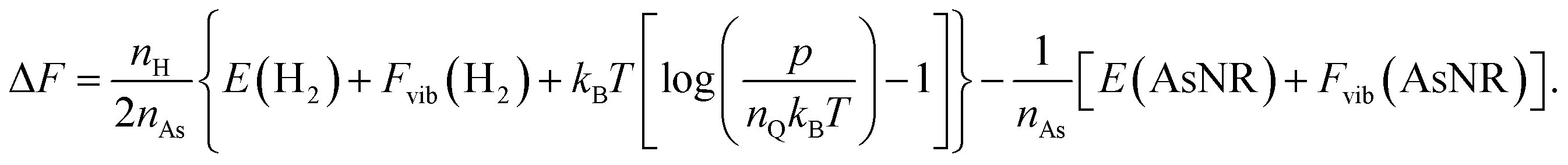
The next step in our assessment of stability, with a special focus on passivated vs. non-passivated comparisons, involves adding in the effect of atomic vibrations to the energetic analysis. As illustrated in ref. 14, this can change the conclusions even at 0 K, and lead to crossovers at finite temperature. Let us consider two generic nanoribbons of types I and II. Each unit cell of type I (II) contains nIAs (nIIAs) arsenic atoms and nIH (nIIH) hydrogen atoms, so the following process is balanced:
 | (2) |
 | (3) |
 | (4) |
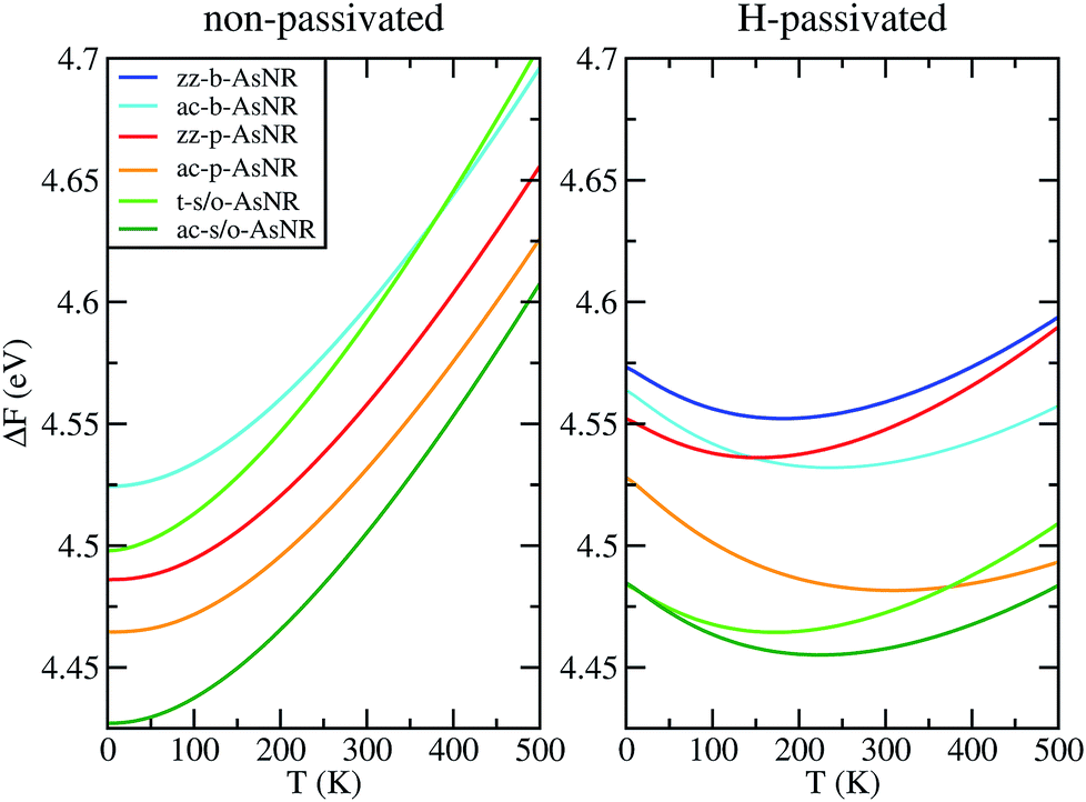 | ||
| Fig. 6 Free energy per arsenic atom of the passivated and non-passivated AsNRs shown in Fig. 1 as a function of temperature, as defined in the text. | ||
3 Conclusions
To sum up, our results show that many of the AsNRs considered here are wide-bandgap semiconductors, i.e., have gaps in the 2–4 eV range. Therefore, they are good candidates for the design of new semiconductor devices able to operate at much higher voltages, frequencies and temperatures than conventional semiconductors like Si. In particular, all t-s/o-AsNRs have band gaps around 3 eV, the highest among all the non-passivated ribbons; most ac-b-AsNRs have band gaps between 2 and 2.5 eV; and all H-t-s/o-AsNRs, H-ac-b-AsNRs, H-zz-b-AsNRs and H-ac-s/o-AsNRs, as well as the thinnest H-zz-p-AsNRs and H-ac-p-AsNRs, fall within the 2–4 eV band gap range. Non-passivated ribbons (t-s/o-AsNRs and ac-b-AsNRs, also the most stable according to free-energy calculations) are more relevant at high T, since the stabilization due to edge passivation is overcome by thermal activation of vibrational modes involving the H atoms. Besides, when deposited on an inert substrate to build an electronic device, edge passivation by means of H is not commonly sought. In that regard, it is worth noting that the stability of these nanostructures can be further enhanced when grown on appropriate substrates. With an eye put on miniaturization and low-dimensionality, t-s/o-AsNRs deserve particular attention. Our results show that they can be seen as an array of weakly interacting nanowires, a fact that points to the possibility of reaching the thinnest stable nanoribbon so far.Conflicts of interest
There are no conflicts to declare.Acknowledgements
This work was supported by the Xunta de Galicia (AGRUP2015/11, ED431E 2018/8 and GRC ED431C 2016/001) and by the Junta de Castilla y León (Project No. VA124G18). The first two of these research projects were partially supported by FEDER.References
- Y. Zhang, A. Rubio and G. L. Lay, J. Phys. D: Appl. Phys., 2017, 50, 053004 CrossRef.
- K. Takeda and K. Shiraishi, Phys. Rev. B: Condens. Matter Mater. Phys., 1994, 50, 14916–14922 CrossRef CAS.
- S. Cahangirov, M. Topsakal, E. Aktürk, H. Şahin and S. Ciraci, Phys. Rev. Lett., 2009, 102, 236804 CrossRef CAS PubMed.
- P. Vogt, P. De Padova, C. Quaresima, J. Avila, E. Frantzeskakis, M. C. Asensio, A. Resta, B. Ealet and G. Le Lay, Phys. Rev. Lett., 2012, 108, 155501 CrossRef.
- M. E. Dávila, L. Xian, S. Cahangirov, A. Rubio and G. L. Lay, New J. Phys., 2014, 16, 095002 CrossRef.
- M. Derivaz, D. Dentel, R. Stephan, M.-C. Hanf, A. Mehdaoui, P. Sonnet and C. Pirri, Nano Lett., 2015, 15, 2510–2516 CrossRef CAS.
- A. H. Castro Neto, F. Guinea, N. M. R. Peres, K. S. Novoselov and A. K. Geim, Rev. Mod. Phys., 2009, 81, 109–162 CrossRef CAS.
- J.-A. Yan, R. Stein, D. M. Schaefer, X.-Q. Wang and M. Y. Chou, Phys. Rev. B: Condens. Matter Mater. Phys., 2013, 88, 121403 CrossRef.
- V. Georgakilas, M. Otyepka, A. B. Bourlinos, V. Chandra, N. Kim, K. C. Kemp, P. Hobza, R. Zboril and K. S. Kim, Chem. Rev., 2012, 112, 6156–6214 CrossRef CAS PubMed.
- L. Li, Y. Yu, G. J. Ye, Q. Ge, X. Ou, H. Wu, D. Feng, X. H. Chen and Y. Zhang, Nat. Nanotechnol., 2014, 9, 372–377 CrossRef CAS PubMed.
- H. Liu, A. T. Neal, Z. Zhu, Z. Luo, X. Xu, D. Tománek and P. D. Ye, ACS Nano, 2014, 8, 4033–4041 CrossRef CAS PubMed.
- Z. Zhu and D. Tománek, Phys. Rev. Lett., 2014, 112, 176802 CrossRef PubMed.
- F. Ersan, E. Aktürk and S. Ciraci, Phys. Rev. B: Condens. Matter Mater. Phys., 2016, 94, 245417 CrossRef.
- J. Carrete, L. J. Gallego and N. Mingo, J. Phys. Chem. Lett., 2017, 8, 1375–1380 CrossRef CAS PubMed.
- S. Zhang, Z. Yan, Y. Li, Z. Chen and H. Zeng, Angew. Chem., Int. Ed., 2015, 54, 3112–3115 CrossRef CAS PubMed.
- C. Kamal and M. Ezawa, Phys. Rev. B: Condens. Matter Mater. Phys., 2015, 91, 085423 CrossRef.
- Y. Wang and Y. Ding, Nanoscale Res. Lett., 2015, 10, 254 CrossRef PubMed.
- J. Zhang, H. J. Liu, L. Cheng, J. Wei, J. H. Liang, D. D. Fan, J. Shi, X. F. Tang and Q. J. Zhang, Sci. Rep., 2014, 4, 6452 CrossRef CAS PubMed.
- H.-S. Tsai, S.-W. Wang, C.-H. Hsiao, C.-W. Chen, H. Ouyang, Y.-L. Chueh, H.-C. Kuo and J.-H. Liang, Chem. Mater., 2016, 28, 425–429 CrossRef CAS.
- G. Kresse and J. Hafner, Phys. Rev. B: Condens. Matter Mater. Phys., 1993, 47, 558–561 CrossRef CAS.
- G. Kresse and J. Furthmüller, Phys. Rev. B: Condens. Matter Mater. Phys., 1996, 54, 11169–11186 CrossRef CAS.
- A. Togo and I. Tanaka, Scr. Mater., 2015, 108, 1–5 CrossRef CAS.
- J. P. Perdew, K. Burke and M. Ernzerhof, Phys. Rev. Lett., 1996, 77, 3865–3868 CrossRef CAS PubMed.
- J. Heyd, G. E. Scuseria and M. Ernzerhof, J. Chem. Phys., 2003, 118, 8207–8215 CrossRef CAS.
- J. Heyd, G. E. Scuseria and M. Ernzerhof, J. Chem. Phys., 2006, 124, 219906 CrossRef.
- J. Paier, M. Marsman, K. Hummer, G. Kresse, I. C. Gerber and J. G. Ángyán, J. Chem. Phys., 2006, 124, 154709 CrossRef CAS PubMed.
- J. Paier, M. Marsman, K. Hummer, G. Kresse, I. C. Gerber and J. G. Ángyán, J. Chem. Phys., 2006, 125, 249901 CrossRef.
- D. Kecik, E. Durgun and S. Ciraci, Phys. Rev. B: Condens. Matter Mater. Phys., 2016, 94, 205409 CrossRef.
- R. Swaroop, P. K. Ahluwalia, K. Tankeshwar and A. Kumar, RSC Adv., 2017, 7, 2992–3002 RSC.
- J. Carrete, W. Li, L. Lindsay, D. A. Broido, L. J. Gallego and N. Mingo, Mater. Res. Lett., 2016, 4, 204–211 CrossRef CAS.
- G. Coloyan, N. D. Cultrara, A. Katre, J. Carrete, M. Heine, E. Ou, J. Kim, S. Jiang, L. Lindsay, N. Mingo, D. Broido, J. P. Heremans, J. Goldberger and L. Shi, Appl. Phys. Lett., 2016, 109, 131907 CrossRef.
Footnote |
| † Electronic supplementary information (ESI) available. See DOI: 10.1039/c9ra00975b |
| This journal is © The Royal Society of Chemistry 2019 |