
 Open Access Article
 This Open Access Article is licensed under a Creative Commons Attribution-Non Commercial 3.0 Unported Licence
Ultrafine nanoparticles of W-doped SnO2 for durable H2S sensors with fast response and recovery†
Pengjian Wang ab,
Junfeng Huia,
Tingbiao Yuanb,
Peng Chenc,
Yue Suc,
Wenjie Liangc,
Fulin Chend,
Xiaoyan Zheng*ad,
Yuxin Zhao*e and
Shi Hu*b
ab,
Junfeng Huia,
Tingbiao Yuanb,
Peng Chenc,
Yue Suc,
Wenjie Liangc,
Fulin Chend,
Xiaoyan Zheng*ad,
Yuxin Zhao*e and
Shi Hu*b
aShaanxi Key Laboratory of Degradable Biomedical Materials, Shanxi R&D Center of Biomaterials and Fermentation Engineering, School of Chemical and Engineering, Northwest University, Xian, Shaanxi 710069, China. E-mail: zy129@126.com
bDepartment of Chemistry, School of Science, Tianjin Key Laboratory of Molecular Optoelectronic Science, Tianjin University, Tianjin 300072, China. E-mail: rychushi@gmail.com
cBeijing National Laboratory for Condensed Matter Physics, Beijing Key Laboratory for Nanomaterials and Nanodevices, Institute of Physics, Chinese Academy of Sciences, Beijing 100190, China
dCollege of Life Sciences, Northwest University, Xian, Shaanxi 710069, China
eState Key Laboratory of Safety and Control for Chemicals, SINOPEC Research Institute of Safety Engineering, No. 339, Songling Road, Laoshan District, Qingdao, Shandong 266071, China. E-mail: zhaoyuxin1@yeah.net
First published on 9th April 2019
Abstract
Ultrafine nanoparticles of W-doped SnO2 with an average diameter of 6 nm were fabricated via a facile hydrothermal method. The material shows a reduced particle size and enhanced response to H2S gas as compared to the pristine SnO2 nanoparticles. The detection limit can be down to 100 ppb while the response time and recovery time of the 5%-doped one are reduced to 17 s and 7 s respectively. In addition, the material shows impressive long-term stability of the response through 40 cycles of injection with 10 ppm H2S, which is attractive for designing a durable hydrogen sulfide sensor. The doping of W results in the reduction of size and modification of the electronic band structure of SnO2, which reduces the response time and recovery time and further improves the sensing durability of the materials.
1. Introduction
With the growth of global oil & gas exploration as well as drying up of high-quality light sweet crude, more sour fields with high sulfur content have to be developed. Therefore, the leakage incidents of highly toxic gas hydrogen sulfide (H2S) during well drilling, pipeline transportation, oil refinement and final discharge have remarkably increased over the past decades. In 2003, the blowout of sour-gas wells in southwestern China, described as the worst accidental H2S emission in history, caused 243 deaths and 64![[thin space (1/6-em)]](https://www.rsc.org/images/entities/char_2009.gif) 000 residents were evacuated from the exposure area, greatly harming the safety of civilians, as well as its further comprehensive influence over time.1 In addition to its health issues, the flammable nature of H2S could also threaten public security owing to the risk of fire and explosion.2 Therefore, the development of efficient and robust H2S sensors for the timely and reliable detection under practical harsh conditions is highly imperative.
000 residents were evacuated from the exposure area, greatly harming the safety of civilians, as well as its further comprehensive influence over time.1 In addition to its health issues, the flammable nature of H2S could also threaten public security owing to the risk of fire and explosion.2 Therefore, the development of efficient and robust H2S sensors for the timely and reliable detection under practical harsh conditions is highly imperative.
To date, various gas sensors have been applied in H2S gas monitoring, such as colorimetric assay,3 chemoresistive sensors,4 electrochemical sensors,5 piezoelectric sensors,6 optical sensors and conducting polymeric sensors,7,8 etc. Among these alternatives, semiconducting metal oxide (SMO) sensors are considered to be the most economical, convenient and efficient with typical detection range in ppm levels.9 Their working principle is based on the electrical variation introduced by the diffusion or chemical reaction of gases/vapors in the coated or deposited sensitive layer. Thus the performance of this solution depends largely on sensing materials. To meet the demands of actual applications, researchers have devoted significant attention to develop H2S sensitive materials, particularly molybdenum trioxide,4 tungsten trioxide,10 cupric oxide,11 zinc oxide12 and stannic oxide13 with a lot of “debugging” possibilities (i.e. size reduction, surface decoration, heterojunction, composite formation, etc.) on purpose.8,14–16 These candidates have shown many advantages, including improved surface catalytic activation, high electron mobility and appropriate contact potential at the interface between components. For example, detection limits of ppb and ppm of H2S were demonstrated using graphene flakes/WO3 nanofibers and Cu–ZnO nanowires, respectively.9,17 However, there still exist several unaddressed scientific and technical challenges. One primary challenge is instability issues of the contact state of sensing interface caused by physical and chemical degrading processes owing to the complex humid environment.18 The presence of acidic corrosive components, dirt particles in the atmosphere as well as intermittent thermal shock, usually cause the failure of elaborated surface functional groups and micro-/nano-architectures during long-term cycling, which leads to loss of active sites and eventual fading of sensing capacity. Another challenge is two essential properties of sensing materials—high response sensitivity and high recovery rate—are contradictory. The strong bonding between target gas and sensing layer at lower concentrations could achieve high sensitivity and selectivity, but also make it harder to desorb gas molecules and hence resulting in sluggish recovery. This problem is particularly acute in “room-temperature” gas sensors, wherein recovery time (t50: time taken for the sensor to recover within 50% of its initial baseline after removal of gas) is generally around several minutes or more with detection ranges of 1–20 ppm, which is insufficient to meet the actual requirement.19,20 Finally, these challenges are compounded with the fact that the synthesis must be easily scaled up and easily integrated with electronics for real-world utilizations.
While there have been exciting progresses in addressing a subset of these challenges, few have sought to address all of these challenges simultaneously. Recently, non-carbon ultrafine nanostructures with further reduced size of sub-10 nm as compared to traditional nanomaterials afford promising opportunities to address all of these challenges. Due to their significant decrease of the thickness, the percentage of surface atoms and active sites exposed can be greatly enhanced, making them highly favourable for surface-dominated adsorption–desorption mass transfer process and chemo-catalysis applications.21,22 Another attractive feature of ultrathin nanomaterials is their unique electronic structures tenability.23 Such external-stimuli sensitive nature allows us to fine tune their electronic properties in a desired manner at a highly controllable level via the use of reticular chemistry, such as chemical modification, doping, and hybridization. The electron confinement in ultrathin materials especially semiconductors, enable greatly compelling electronic properties and concomitant intrinsic bandgap variation, therefore rendering them appealing candidates for electronic device applications and fundamental condensed matter research.24,25 Furthermore, to quantify the atomic thickness that may be attained with effective assembling of ultrathin film monolayers or porous constructs while offering them maximum mechanical flexibility and stability, making them suitable for the integration of reliable and highly flexible semiconductor electrodes in sensing applications.22,26 It is worth noting that doping can effectively change the electronic structure of the SMOs. Thus, doping is the most commonly used methods to enhance the gas sensing performance of SMOs to certain gases. Tungsten, a member of the transition metals element, has a variety of oxidation states. It is expected to be an efficient doping material in the field of gas sensing applications. It has been realized that doping high-valent metal element can effectively improve the gas sensing properties of materials. In addition, the radius of tungsten (W6+: 67 pm) is close to that of tin (Sn4+: 71 pm), and hence W6+ can easily replace Sn4+ in theory.27
Herein, a facile hydrothermal method was demonstrated to grow ultrafine W-doped SnO2 nanoparticles (WS-NPs). As a proof of concept, the uniform distribution of well-decorated NPs without aggregation on SMO sensors and their potential application toward H2S monitoring were demonstrated. Taking advantage of large lateral size with ultrahigh specific surface area, more oxygen adsorption sites and ready gas accessibility, a great improvement in sensitivity and selectivity even toward ppb level of H2S gas can be achieved. Principally, SnO2 nanoparticles with 5% W doping exhibited an ultra-fast response–recovery time sensing to 10 ppm H2S at 260 °C. Furthermore, adsorption/desorption kinetic process on the surface of WS-NPs was also proposed. It is expected that these ultrafine NPs are promising for a real-time monitoring of trace H2S in oil/gas platforms and refineries, as well as in manufacturing processes and fire-fighting.
2. Experimental procedure
2.1 Chemicals
Tin(II) chloride dihydrate (SnCl2·2H2O), absolute ethanol were purchased from Sinopharm Chemical Reagent Co. Ltd. Urea was purchased from Aladdin Chemical Reagent Co. Ltd. Tungsten hexachloride (WCl6) was purchased from Shanghai Macklin Biochemical Co. Ltd. All chemicals were used as received without further purification. Deionized water was used throughout the experiments.2.2 Synthesis of materials
SnO2 nanoparticles were synthesized by a facile hydrothermal process followed by calcination. In a typical synthesis procedure, 0.04 g of SnCl2·2H2O and 0.01 g of urea were added into 40 ml of deionized water and the mixture was then stirred for 30 min to form a homogeneous solution. Afterward, the reaction solution was transferred to a 50 ml Teflon-lined stainless-steel autoclave and kept in an oven at 180 °C for 24 h. After naturally cooling down to room temperature, the product was collected by centrifugation, rinsed with distilled water and absolute ethanol for several times, and dried at 60 °C for 12 h. The obtained intermediate product was further calcinated at 500 °C for 2 h with a heating rate 5 °C min−1 to obtain the final product.W-doped SnO2 nanoparticles were synthesized with a similar procedure as follows. First, an appropriate amount of WCl6 was added to 20 ml of absolute ethanol. After 5 min of stirring, 0.04 g of SnCl2·2H2O and 0.01 g of urea were added into the homogeneous solution and then transferred into a 50 ml Teflon-lined autoclave which was sealed and kept at 180 °C for 24 h. The amount of WCl6 was calculated according to the atomic weight ratio: W/SnO2 = 0%, 1%, 2.5%, 5%, 7.5%, 10%. After cooling down to room temperature, the solid products were collected using the same process described above and dried at 60 °C for 12 h. Finally, all samples were calcinated at 500 °C in air for 2 h before the following characterization. The pristine and W-doped SnO2 nanoparticles with different doping concentrations of 0, 1, 2.5, 5, 7.5, 10% were synthesized and labelled as WS-0, WS-1, WS-2.5, WS-5, WS-7.5 and WS-10, respectively.
2.3 Fabrication and measurement of gas sensors
The gas sensing property of the materials were tested by the following steps. First, the samples were mixed with terpineol and uniformly coated on the surface of alumina ceramic tube with a heating resistor of Ni–Cr alloy going through the hollow part of the ceramic tube and a pair of gold electrodes attached on the surface and connected by Pt wires.28 The coated tube was left to age at 400 °C for 48 h to burn off the terpineol. The material became porous with the resistance stabilized during aging before it was tested on a computer-controlled gas-sensing system (WS-30A by Winson Electronics Co., Ltd., Zhengzhou, China). In the sensing test process, an appropriate bias voltage (Vc = 5 V) was applied. The whole test environment was in the air atmosphere (12–17 °C) with a humidity level controlled at 30–40%.The gas response is defined as Ra/Rg (Ra and Rg are the electric resistance of the sensors in air and in the target gas, respectively).29,30 The response time (tres) is defined as the time for the resistance to reach 90% of the final stable output after the injection of target gas, while the recovery time (trec) is defined as the time to fall to 10% of its maximum output after the target gas was discharged.14,28,31
3. Results and discussion
3.1 Morphology and structure
The crystal structure of all the samples were reflected by their XRD patterns with well-resolved diffraction peaks in the range from 20° to 80°. As shown in Fig. 1, all the peaks can be assigned to SnO2 of cassiterite structure (JCPDS: 41-1445) and no diffraction peaks from the oxides of tungsten were detected for the W-doped SnO2 up to the doping level of 10%. No sign of oxide of tungsten could be identified from this series of patterns, indicating good dispersion of tungsten in SnO2 lattice, which could be attributed to the similar radius of Sn4+ (71 pm) with W6+ (67 pm). It should be noted that the size of the nanocrystallite shows a decreasing trend with the increase of doping level, as indicated by the widening of the diffraction peaks. Applying Scherrer equation to the full width at half maximum (FWHM) of (110) peaks yields a crystal size of 15.6 nm for undoped SnO2 against 7.6 nm for 5% W-doped SnO2 and 6.6 nm for 10% W-doped SnO2. Similar results can be obtained with 14.8 nm against 7.1 nm and 6.6 nm for (101) diffraction and 12.6 nm against 7.1 nm and 6.1 nm for (211) diffractions. It is worth noting that, the pristine SnO2 after hydrothermal synthesis contains SnO (JCPDS card no. 85-0712), as is shown in Fig. S1.† It is eliminated through further annealing process while the W-doped sample completely converts to SnO2 even before the annealing. This could be attributed to the oxidative effect of W(VI) species in the hydrothermal system.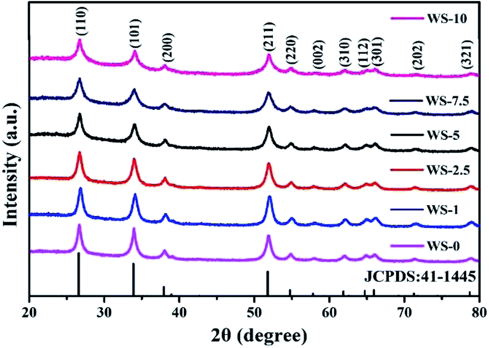 | ||
| Fig. 1 XRD pattern of the pristine SnO2 and W-doped SnO2 nanoparticles with increasing doping level. | ||
The morphology and crystal structure of the pristine SnO2 nanoparticles are further inspected with SEM, TEM and HRTEM, as shown in Fig. S2,† 2a and b. The pristine SnO2 are composed of nanoparticles with diameter from 6 to 20 nm (Fig. 2a and b) and clear lattice fringes can be identified with layer spacing of 0.334 and 0.262 nm, corresponding to the (110) and (101) diffraction of cassiterite SnO2. The TEM image of WS-5 nanoparticles in Fig. 2c indicates that the doped sample WS-5 has a reduced uniform size distribution with diameter of about 6 nm. The HRTEM image in Fig. 2d further shows the lattice fringes of individual WS-5 particles with a layer spacing of 0.334 nm and 0.264 nm rising from the (110) and (101) crystal planes of cassiterite SnO2 respectively. The observed size distribution and peak assignment agree well with the results from XRD patterns. The STEM-EDX mapping of the WS-5 sample in Fig. 2e–h clearly shows the uniform distribution of O, Sn and W, indicating the good doping effect of W element. The decreased size in SnO2 nano-crystallite after doping leads to enhanced surface area and more gas adsorption sites, which could improve the sensitivity to the target gas.
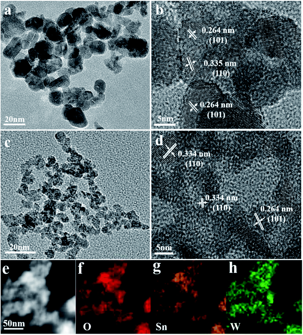 | ||
| Fig. 2 (a and b) TEM and HRTEM images of pristine SnO2 nanoparticles WS-0; (c and d) TEM and HRTEM images of doped SnO2 nanoparticles WS-5; (e) the STEM and (f–h) EDS elemental mapping of WS-5. | ||
The surface chemical states of the pristine SnO2 and W-doped SnO2 were examined by X-ray photoelectron spectroscopy (XPS). As shown in the full spectrum survey of Fig. 3a, the Sn 3d, O 1s and W 4f can be detected, confirming the presence of the W component in the WS-5, which is in agreement with the results of EDS mapping. As shown in Fig. 2b, the peaks of W 4f7/2 at 36.5 eV and W 4f5/2 at 38.6 eV can be assigned to the existence of the W(VI) chemical state. The O 1s peak at 530.7 eV and 532.0 eV in pristine SnO2 and WS-5 sample as shown in Fig. 3c. The Sn 3d XPS spectra of WS-0 and WS-5 can be assigned to Sn4+ of bulk SnO2.32 Note that the two Sn 3d peaks of WS-0 (Sn 3d3/2 = 495.2 eV, Sn 3d5/2 = 486.8 eV) are shifted to a lower binding energy in WS-5 (Sn 3d3/2 = 495.0 eV, Sn 3d5/2 = 486.6 eV), which are caused by the replacement of Sn4+ by W6+ that decreases the binding energy of Sn. The vibration spectra of the samples were further investigated, as is shown in the Raman spectra of Fig. S3.† With the doping of W, the vibration of bond displayed typically decrease in strength, which is caused by the disturbance of the SnO2 lattice by tungsten incorporation and size reduction. Meanwhile, two peaks arise at 942 cm−1 and 992 cm−1, which are believed to come from the vibration of surface W–O complex.33
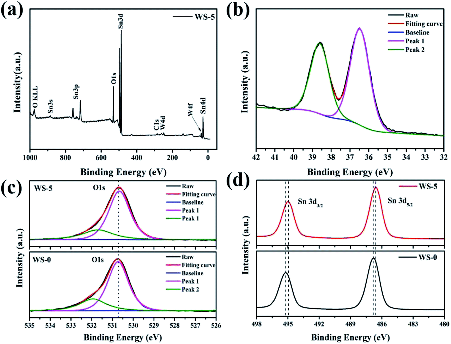 | ||
| Fig. 3 (a) The full XPS survey graph of WS-5; (b) W 4f XPS spectra of WS-5; (c) XPS O 1s and (d) Sn 3d spectra of WS-0 and WS-5. | ||
3.2 Gas sensing properties
While gas sensing is based on the charge carrier change caused by the adsorption and desorption events, the gas-sensing performance of the materials are significantly influenced by the operation temperature. The response of SnO2 and W-doped SnO2 towards 10 ppm H2S gas were evaluated at different operating temperature from 160 °C to 400 °C and the response gradually decreases with the increasing temperature, as shown in Fig. 4a. At 160 °C, all the doped SnO2 showed higher response than the pristine one with the highest response of 87 coming from WS-5 (Fig. S4†). Besides sensitivity, response time and recovery time are equally important parameters for designing gas sensors, which are relatively long at low temperature and short at high temperature. Fig. 4b shows the response time and recovery time of WS-0 and WS-5 versus 10 ppm hydrogen sulfide over the operating temperature range with complete data for all doped samples shown in Fig. S5.† With most of the response time falling below 50 s, the shortest time of 17 s comes from WS-5 at 260 °C. While the response time of all samples are relatively close and not susceptible to varying temperature, the recovery time of the samples are extremely sensitive to the temperature. No sample is capable of recovering to 90% of the baseline resistance within 300 s at the low temperature of 160 °C, impeding the real-time gas response which requires reasonably fast recovery. Meanwhile, the recovery time of all samples could be decreased significantly by increasing the operating temperature to 260 °C with the best performance of only 7 s from WS-5.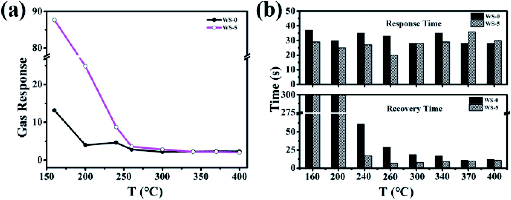 | ||
| Fig. 4 (a) Gas response of SnO2 and W-doped SnO2 to H2S at various temperatures from 160 °C to 400 °C; (b) response time and recovery time of the WS-0 and WS-5 nanoparticles upon exposure to 10 ppm H2S gas at an operating temperature from 160 °C to 400 °C. | ||
The rapid response and recovery process at 260 °C is due to rapid surface chemistry reaction, higher electron mobility and increased gas diffusion rate. In addition, the formation of oxygen adsorbed at high temperature may be from O2− to O2−, O2− + 3e− → 2O2−(ads).34 However, further increase in operating temperature could not shorten the response and recovery time significantly, as shown in Fig. 4b. Reduced power consumption afforded by low temperature and quick response and recovery afforded by high temperature should strike a balance in term of applications in industry. In this considerations, 260 °C was chosen as the optimum operating temperature and WS-5 was chosen as the optimum sample for the following investigation.
The sensing performances of different sensors to H2S is summarized in Table 1. As compared to other reports, the W-doped SnO2 in this report not only significantly decrease respond time and recovery time, but also enhance the SnO2 based sensor with excellent reversibility and stability.
| Materials | Concentration (ppm) | Response (Ra/Rg) | Working temperature (°C) | tres/trec (s) | Ref. |
|---|---|---|---|---|---|
| SnO2 nanocrystals | 5 | 1.6 | 275 | 15/62 | 35 |
| Au–SnO2 hollow spheres | 5 | 17.4 | 400 | 18/— | 36 |
| Au-embedded WO3 nanowire | 10 | 18 | 291 | 27/230 | 37 |
| Au–SnO2 NTs | 5 | 34 | 300 | ∼35/— | 38 |
| rGO-SnO2 NFs | 5 | 33.7 | 200 | ∼115/∼110 | 39 |
| Mo-doped ZnO nanowires | 5 | 14 | 300 | 20/223 | 40 |
| W–SnO2 | 10 | 3.6 | 260 | 17/7 | This work |
The typical response and recovery curve of WS-5 to 10 ppm H2S at operation conditions was shown in Fig. 5a with a response time of 17 s and recovery time of 7 s, respectively. The response of WS-5 to different concentrations of hydrogen sulfide was shown in Fig. 5b, with the lowest concentration at 100 ppb, indicating the low detection limit of the material. For practical application, robustness and stability of the sensor is the most important factor to be considered. Materials need to be inactivate at H2S atmosphere. The response of WS-5 to 10 ppm H2S become stable after 10 cycles as shown in Fig. S6.† The sensing stability of WS-5 was evaluated at 260 °C by repetitive injection of 10 ppm H2S and exposure to air during which the resistance of the sensing materials was recorded. As is shown in Fig. 5c and d, the sensor retains constant response and resistance through 40 cycles of H2S injection and air exposure with no sign of performance degradation. In contrast, the gas response of WS-0 varies significantly and the baseline resistance reading is hard to stabilize within the first 40 cycles. Furthermore, the long-term stability of WS-5 was also investigated. As can be seen in Fig. S7,† WS-5 shows excellent stability in the daily cycle test, and the sensitivity to H2S remains almost unchanged during the 10 day evaluation period.
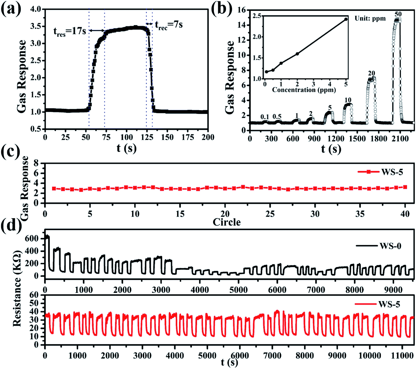 | ||
| Fig. 5 (a) Real-time gas sensing transients of the sensor based on WS-5 to 10 ppm H2S at 260 °C; (b) gas response of WS-5 to various concentration H2S gas ranging from 0.1 ppm to 50 ppm; (c) gas-response reading of the sensor based WS-5 to 10 ppm H2S at 260 °C; (d) 40 cycles of the sensor based on WS-0 and WS-5 to 10 ppm H2S at 260 °C. | ||
As shown in Fig. 6, the response of WS-0 and WS-5 to hydrogen (100 ppm), ammonia (10 ppm), methane (2000 ppm), and carbon monoxide (100 ppm) is compared at the same temperature of 260 °C. Both WS-0 and WS-5 show no response to methane and carbon monoxide, and smaller response to 100 ppm of hydrogen and 10 ppm of ammonia. In addition, WS-5 shows an improved selectivity to hydrogen sulfide than to the other gases.
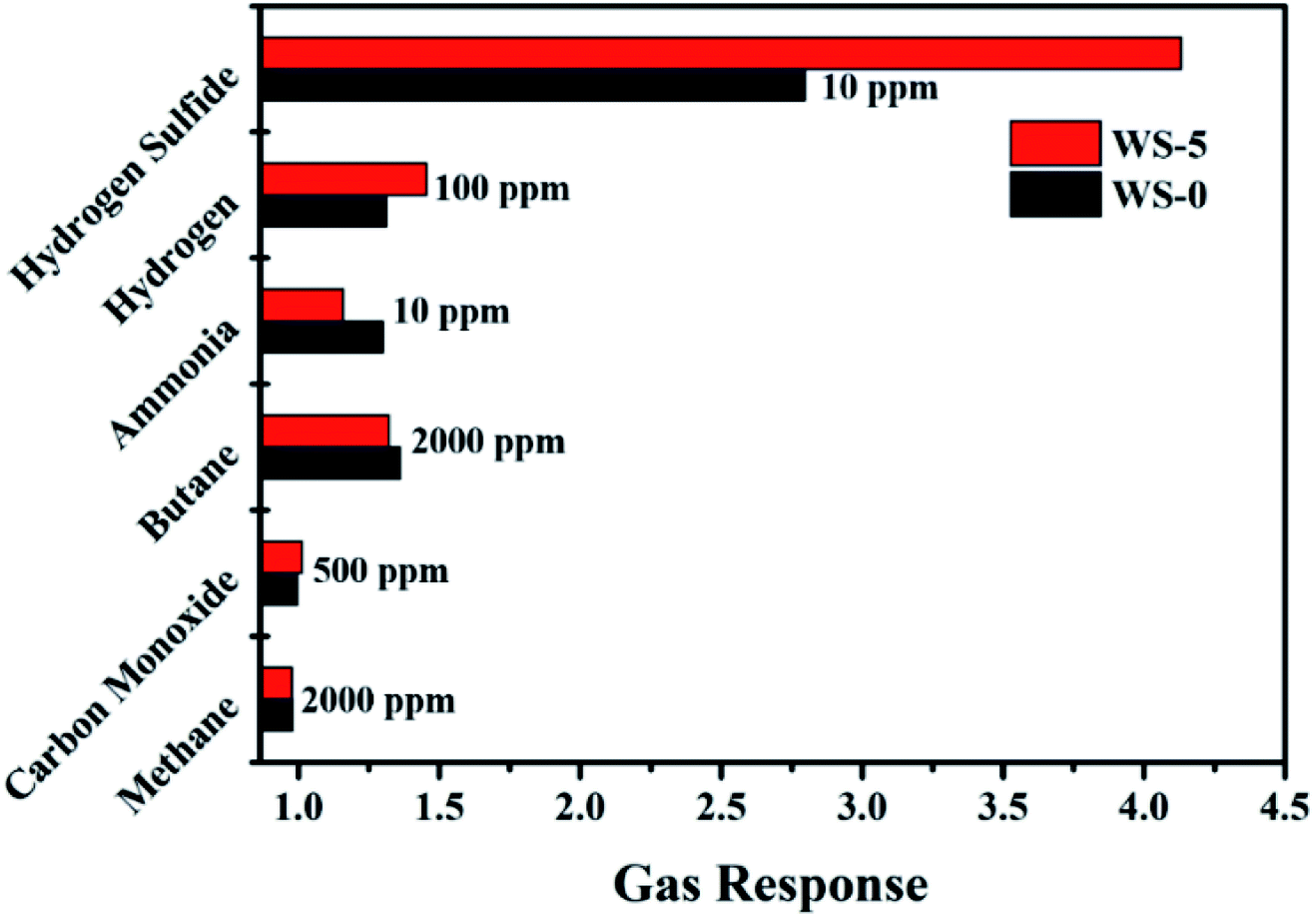 | ||
| Fig. 6 Response of WS-0 and WS-5 sensor exposed to several gases at 260 °C. | ||
3.3 The gas sensing mechanism
Based on the above results, the morphology and structure of the material have deep impact on the response to the adsorbed gas. The morphology of W-doped SnO2 has changed significantly with the particles size decreasing from 15 nm to 6 nm, providing more specific area. In addition, the surface-adsorption induced charge-depletion will lead to increased ratio of charge-depletion volume and more significant variation of the resistance upon sensing. Therefore, the increase in gas sensitivity of WS-5 is mainly attributed to tungsten doping.41 Besides, the XRD patterns from all samples with doping level of 1% to 10% do not show the presence of tungsten oxide phase, indicating that W6+ is doped into the lattice of SnO2, thanks to the similar ion radius of W6+ and Sn4+. The aliovalent doping creates abundant adsorption sites on the surface of SnO2 for O2 and H2S, and induced further change in the band structure which amy also contribute to the faster adsorption/desorption.42As a typical n-type semiconductor, the band structure of SnO2 is not altered from the flat-band situation when there is no electron transfer between the adsorbed molecules and the conduction band at the surface, as shown in Scheme 1a. According to the surface-depletion model, chemisorption of oxygen (O2) on the surface of sensing materials upon exposure to the air extracts the free electrons from the conduction band and traps them at the surface by forming chemisorbed oxygen species (O2−, O−, O2−),42,43 as shown in Scheme 1b. This would result in the formation of a space-charge layer and upward band bending near the surfaces. The potential barrier increases resistance via restricting the flow of electrons.41 Different types of oxygen uptake depend on the operating temperature. When the temperature is lower than 100 °C, O2− usually undergoes chemical reactions. However, when the temperature ranges from 100 to 300 °C, O− becomes a common chemical reaction and O2− disappears rapidly. Oxygen species mainly exist in the form of O2− when the temperature exceeds 300 °C.44 The reaction can be described by the following steps.45–47
| O2(gas) → O2(ads) | (1) |
| O2(ads) + e− → O2−(ads), (T < 100 °C) | (2) |
| O2−(ads) + e− → 2O−(ads), (100 °C < T < 300 °C) | (3) |
| O−(ads) + e− → O2−(ads), (T > 300 °C) | (4) |
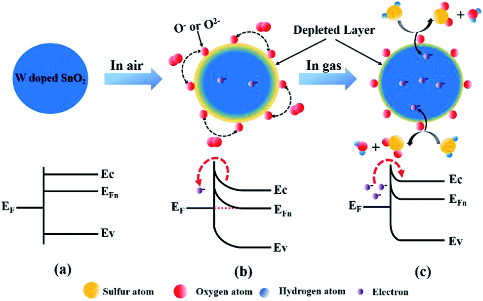 | ||
| Scheme 1 Schematic images and band diagrams of the surface reactions in different atmosphere: (a) in Ar; (b) exposed to air; (c) in air with the presence of H2S gas. Ec: conduction band; EF: redox potential of adsorbed molecules; EFn: Fermi level in the n-type semiconductor; Ev: valence band. | ||
At the operating temperature of 260 °C, the mainly adsorbed oxygen are O2− and O−. Once the sensor was exposed to the H2S gas, these adsorbed oxygen (O2−, O−) would react with H2S molecules to form SO2 and water vapor. In this process, the captured electrons are released back into the depletion layer. Therefore, the depletion layer will shrink and the resistance of WS-5 reduced (Scheme 1c). This chemical reaction can be described below:
| H2S(gas) + O−(ads) → SO2(gas) + H2O(gas) + e− |
Adsorbed oxygen ions (O2−, O− or O2−) are known to be the most common surface species in SMOs.28 The introduction of aliovalent tungsten atoms actually increase the conductivity by further modifying the electronic band structure of SnO2 and hence improves the reversibility of H2S adsorption and desorption, which in turn improves the H2S durability of the sensor. As for the asymmetric variation of response and recovery time with the temperature, it is attributed to the different pathways in adsorption and desorption. A series of complicated processes will take place which can be briefly divided into gas-phase diffusion and surface-reaction. The kinetics of a tandem process is usually determined by the rate of the slowest reaction which may differ in the response and recovery process.48 However, our discussion is far from satisfactory and further experiments are needed to fully illustrate the picture behind the complicated sensing behavior.
4. Conclusions
A simple hydrothermal method was used to obtain W-doped tin dioxide nanoparticles of about 6 nm. In the operating temperature from 160 °C to 400 °C, 5% W-doped SnO2 shows the best response to 10 ppm H2S at 260 °C. The synergistic effect of tungsten doping and size reduction of SnO2 crystallites have a great influence on the structure and gas performance of the materials. Compared with pristine SnO2, 5% W-doped SnO2 exhibits enhanced gas sensitivity down to 100 ppb of H2S while the response time and recovery time can be reduced to 17 s and 7 s, respectively. Most importantly, the W-doped SnO2 shows an extraordinary stability with almost unchanged baseline resistance and response resistance after 40 circles and 10 days tested. The enhanced gas sensing performance is mainly due to the decreased particle size of W-doped SnO2, increased specific surface area and the doping-modified electronic structure. We hope our endeavor in the highly-durable H2S sensor will provide useful guidance for the other gas-sensing materials with extraordinary performance for industrial applications.Conflicts of interest
There are no conflicts to declare.Acknowledgements
This work was financially supported by the National Science Foundation of China under No. 21601133, 21676215 and 61701543, China Postdoctoral Science Foundation (2018M633556) and Sinopec Innovation Scheme under A-381.Notes and references
- D. Yang, G. Chen and R. Zhang, Aerosol Air Qual. Res., 2006, 6, 430–443 CrossRef CAS.
- S. K. Pandey, K. H. Kim and K. T. Tang, Trends Anal. Chem., 2012, 32, 87–99 CrossRef CAS.
- Z. Gao, D. Tang, D. Tang, R. Niessner and D. Knopp, Anal. Chem., 2015, 87, 10153–10160 CrossRef CAS PubMed.
- M. Malekalaie, M. Jahangiri, A. M. Rashidi, A. Haghighiasl and N. Izadi, Mater. Sci. Semicond. Process., 2015, 38, 93–100 CrossRef CAS.
- M. Govindhan, B.-R. Adhikari and A. Chen, RSC Adv., 2014, 4, 63741–63760 RSC.
- Y. Nie, P. Deng, Y. Zhao, P. Wang, L. Xing, Y. Zhang and X. Xue, Nanotechnology, 2014, 25, 265501 CrossRef PubMed.
- J. Shu, Z. Qiu and D. Tang, Anal. Chem., 2018, 90, 9691–9694 CrossRef CAS PubMed.
- P. G. Su and Y. T. Peng, Sens. Actuators, B, 2014, 193, 637–643 CrossRef CAS.
- D. R. Miller, S. A. Akbar and P. A. Morris, Sens. Actuators, B, 2014, 204, 250–272 CrossRef CAS.
- D. H. Kim, J. S. Jang, W. T. Koo, S. J. Choi, H. J. Cho, M. H. Kim, S. J. Kim and I. D. Kim, ACS Sens., 2018, 3, 1164–1173 CrossRef CAS PubMed.
- Y. Fu, Y. Zhao, P. Wang, L. Xing and X. Xue, Phys. Chem. Chem. Phys., 2014, 17, 2121–2126 RSC.
- J. Kim and K. Yong, J. Phys. Chem. C, 2011, 115, 7218–7224 CrossRef CAS.
- S. C. Lee, B. W. Hwang, S. Y. Kim, J. H. An, S. Y. Jung, J. S. Huh, D. D. Lee and J. C. Kim, J. Nanoelectron. Optoelectron., 2015, 10, 460–465 CrossRef CAS.
- Y. Wang, B. Liu, S. Xiao, X. Wang, L. Sun, H. Li, W. Xie, Q. Li, Q. Zhang and T. Wang, ACS Appl. Mater. Interfaces, 2016, 8, 9674–9683 CrossRef CAS PubMed.
- Q. Zhou, W. Chen, L. Xu, R. Kumar, Y. Gui, Z. Zhao, C. Tang and S. Zhu, Ceram. Int., 2018, 44, 4392–4399 CrossRef CAS.
- G. J. Sun, S. W. Choi, A. Katoch, P. Wu and S. K. Sang, J. Mater. Chem. C, 2013, 1, 5454–5462 RSC.
- S. J. Choi, C. Choi, S. J. Kim, H. J. Cho, M. Hakim, S. Jeon and I. D. Kim, Sci. Rep., 2015, 5, 8067 CrossRef CAS PubMed.
- K.-I. Choi, H.-J. Kim, Y. C. Kang and J.-H. Lee, Sens. Actuators, B, 2014, 194, 371–376 CrossRef CAS.
- Z. Song, Z. Wei, B. Wang, Z. Luo, S. Xu, W. Zhang, H. Yu, M. Li, Z. Huang, J. Zang, F. Yi and H. Liu, Chem. Mater., 2016, 28, 1205–1212 CrossRef CAS.
- Z. Li, N. Wang, Z. Lin, J. Wang, W. Liu, K. Sun, Y. Q. Fu and Z. Wang, ACS Appl. Mater. Interfaces, 2016, 8, 20962–20968 CrossRef CAS PubMed.
- Y. Sun, S. Gao, F. Lei and Y. Xie, Chem. Soc. Rev., 2015, 44, 623–636 RSC.
- J. Shu, Z. Qiu, Q. Zhou and D. Tang, Chem. Commun., 2019, 55, 3262–3265 RSC.
- H. Zhang, ACS Nano, 2015, 9, 9451–9469 CrossRef CAS PubMed.
- U. N. Maiti, W. J. Lee, J. M. Lee, Y. Oh, J. Y. Kim, J. E. Kim, J. Shim, T. H. Han and S. O. Kim, Adv. Mater., 2014, 26, 40–67 CrossRef CAS PubMed.
- L. Peng, X. Peng, B. Liu, C. Wu, Y. Xie and G. Yu, Nano Lett., 2013, 13, 2151–2157 CrossRef CAS PubMed.
- Y. Al-Hadeethi, A. Umar, S. H. Al-Heniti, R. Kumar, S. H. Kim, X. Zhang and B. M. Raffah, Ceram. Int., 2017, 43, 2418–2423 CrossRef CAS.
- Y. Huang, G. Li, J. Feng and Q. Zhang, Thin Solid Films, 2010, 518, 1892–1896 CrossRef CAS.
- J. Hu, T. Wang, Y. Wang, D. Huang, G. He, Y. Han, N. Hu, Y. Su, Z. Zhou and Y. Zhang, Sens. Actuators, B, 2018, 263, 120–128 CrossRef CAS.
- Z. Dai, L. Xu, G. Duan, T. Li, H. Zhang, Y. Li, Y. Wang, Y. Wang and W. Cai, Sci. Rep., 2013, 3, 1669 CrossRef PubMed.
- W. Zhang, X. L. Cheng, X. Zhang, Y. Xu, S. Gao, H. Zhao and L. Huo, Sens. Actuators, B, 2017, 247, 664–672 CrossRef CAS.
- X. Liu, N. Chen, B. Han, X. Xiao, G. Chen, I. Djerdj and Y. Wang, Nanoscale, 2015, 7, 14872–14880 RSC.
- S. Cui, Z. Wen, E. Mattson, S. Mao, J. Chang, M. Weinert, C. Hirschmugl, M. Gajdardziskajosifovska and J. Chen, Mater. Sci. Eng., C, 2013, 1, 4462–4467 CAS.
- A. A. El-Kheshen, F. H. El-Batal and S. Y. Marzouk, Indian J. Pure Appl. Phys., 2008, 46, 225–238 CAS.
- Y. Wang, B. Liu, S. Xiao, H. Li, L. Wang, D. Cai, D. Wang, Y. Liu, Q. Li and T. Wang, J. Mater. Chem. A, 2015, 3, 1317–1324 RSC.
- M. Lin, Y. Chen and J. Ma, Sci. Rep., 2014, 4, 6028 Search PubMed.
- S. J. Choi, M. P. Kim, S. J. Lee, B. J. Kim and I. D. Kim, Nanoscale, 2014, 6, 11898–11903 RSC.
- N. Minh Vuong, D. Kim and H. Kim, Sci. Rep., 2015, 5, 11040 CrossRef PubMed.
- J.-S. Jang, S.-J. Kim, S.-J. Choi, N.-H. Kim, M. Hakim, A. Rothschild and I.-D. Kim, Nanoscale, 2015, 7, 16417–16426 RSC.
- S.-J. Choi, B.-H. Jang, S.-J. Lee, B. K. Min, A. Rothschild and I.-D. Kim, ACS Appl. Mater. Interfaces, 2014, 6, 2588–2597 CrossRef CAS PubMed.
- H. S. Woo, C. H. Kwak, I. D. Kim and J. H. Lee, J. Mater. Chem. A, 2014, 2, 6412–6418 RSC.
- J. Shu, Z. Qiu, S. Lv, K. Zhang and D. Tang, Anal. Chem., 2017, 89, 11135–11142 CrossRef CAS PubMed.
- Z. Li, Y. Huang, S. Zhang, W. Chen, K. Zhong, D. Ao, L. Wei and Y. Fu, J. Hazard. Mater., 2015, 300, 167–174 CrossRef CAS PubMed.
- L. Xu, R. Xing, J. Song, W. Xu and H. Song, J. Mater. Chem. C, 2013, 1, 2174–2182 RSC.
- C. Shoou-Jinn, H. Ting-Jen, C. I-Cherng and H. Bohr-Ran, Nanotechnology, 2008, 19, 175502 CrossRef PubMed.
- X. Kou, C. Wang, M. Ding, C. Feng, X. Li, J. Ma, H. Zhang, Y. Sun and G. Lu, Sens. Actuators, B, 2016, 236, 425–432 CrossRef CAS.
- W. Yang, P. Wan, X. Zhou, J. Hu, Y. Guan and L. Feng, Sens. Actuators, B, 2014, 201, 228–233 CrossRef CAS.
- H. Liu, S. P. Gong, Y. X. Hu, J. Q. Liu and D. X. Zhou, Sens. Actuators, B, 2009, 140, 190–195 CrossRef CAS.
- Z. Boroun, M. Ghorbani, A. Moosavi and R. Mohammadpour, J. Phys. Chem. C, 2016, 120, 7678–7684 CrossRef CAS.
Footnote |
| † Electronic supplementary information (ESI) available. See DOI: 10.1039/c9ra00944b |
| This journal is © The Royal Society of Chemistry 2019 |