
 Open Access Article
 This Open Access Article is licensed under a Creative Commons Attribution-Non Commercial 3.0 Unported Licence
Photocontrolled organic field effect transistors based on the fullerene C60 and spiropyran hybrid molecule†
A. R. Tuktarov *a,
R. B. Salikhovb,
A. A. Khuzina,
N. R. Popod'koa,
I. N. Safargalinb,
I. N. Mullagalievb and
U. M. Dzhemileva
*a,
R. B. Salikhovb,
A. A. Khuzina,
N. R. Popod'koa,
I. N. Safargalinb,
I. N. Mullagalievb and
U. M. Dzhemileva
aInstitute of Petrochemistry and Catalysis, Russian Academy of Sciences, Russian Federation. E-mail: tuktarovar@gmail.com
bDepartment of Infocommunication Technologies and Nanoelectronics, Bashkir State University, Russian Federation
First published on 8th March 2019
Abstract
Photocontrolled organic field-effect transistors (OFETs) containing a hybrid compound of fullerene C60 (n-semiconductor) with spiropyran (electrical conductivity photocontroller) as the active layer were fabricated for the first time. It was found that an OFET based on the hybrid compound, unlike the multilayer transistor (a device based on unmodified fullerene C60 and spiropyran in different layers), has higher transfer characteristics (source-to-drain current), charge carrier mobility in the active layer, and response rate to external influence, which makes them promising materials for the manufacture of optical memory elements.
Introduction
The development of organic electronics may bring a broad range of new devices (displays, integrated circuits, sensors, etc.) in the near future. These devices will be ultrathin, lightweight, flexible, and transparent, which will open up new applications inaccessible to traditional silicon-based electronics. One of the promising devices for organic electronics is an organic field effect transistor (OFET) with a transport layer having a thickness of not greater than ten nanometers, in which the flow of charge carriers is controlled by changing the charge density in an electric field.1,2 In most organic materials, especially those used to create electronic devices, the hole conductivity prevails above the electronic conductivity. Therefore, searching for organic materials to create electronic conduction channels is the actual problem. Fullerenes functioning as n-dopants for organic materials occupy a special place among organic semiconductors for OFETs.3 Combining methods for the fabrication of organic transport layers with doping of the initial material with fullerenes would substantially increase the charge carrier concentration and, hence, increase the transistor currents (power of the device). Hence, this is a quite strong possibility to increase both the carrier mobility of an organic field-effect transistor to 102 cm2 V−1 s−1 (extend the frequency range with simultaneous decrease in the controlled voltage level) and to increase the controlled current density (organic transistor power).Fullerene C60 and its cyclopropane derivative PC[60]BM are the most promising and in-demand n-type semiconductor materials for organic electronics.4 The use of fullerene C60 as an active element of low-voltage thin film transistors gives rise to devices with high performance characteristics. This is due to the fact that C60 forms isotropic solids and fullerene-based films can be fabricated without special control of molecular assembly, unlike films of other organic semiconductors.5
Simultaneously, the introduction of a photosensitive film (e.g., based on hetarylethenes, spirophotochromes, or azobenzene) at the boundary between the semiconductor (fullerene) and insulator layers may give low-voltage photocontrolled OFETs and provide a promising approach to multi-bit optical memory devices possessing good electrical characteristics and operation stability and reliability. This approach is currently actively used by various researchers,6–11 but the fabrication of devices is quite costly. Furthermore, the switching efficiency decreases as a result of photodegradation of the photochromic molecule and the presence of a large number of layers, which reduces the number of photons that reach the photochromic molecule.12
Although great experience in the design of light-controlled OFETs and the synthesis and studies of various photochromic compounds has been accumulated in the world practice, the preparation of efficient photochromic systems promising for micro- and nanoelectronics, in particular, for the fabrication of molecular transistors and 3D optical memory elements is still an important challenge of the theoretical and practical organic chemistry and organic materials science. Meanwhile, it is unknown what characteristics will be inherent in the devices with key elements represented by photochromic fullerene-based hybrid molecules, highly promising for organic electronics.
Result and discussion
In view of the above and as a continuation of our research towards the preparation and studies of properties of hybrid molecules based on fullerenes and photochromic compounds aimed at the design of more efficient and promising organic electronic devices,13–18 we have fabricated and investigated a photocontrolled OFET containing pyrrolidinofullerene 1 as the active layer (Fig. 1a).13 Simultaneously, for strict and objective comparison of our results with published data, we have fabricated a multilayer transistor, in which the semiconductor (fullerene C60) and the light-controlled compound (spiropyran SpOx) formed separate layers (Fig. 1b).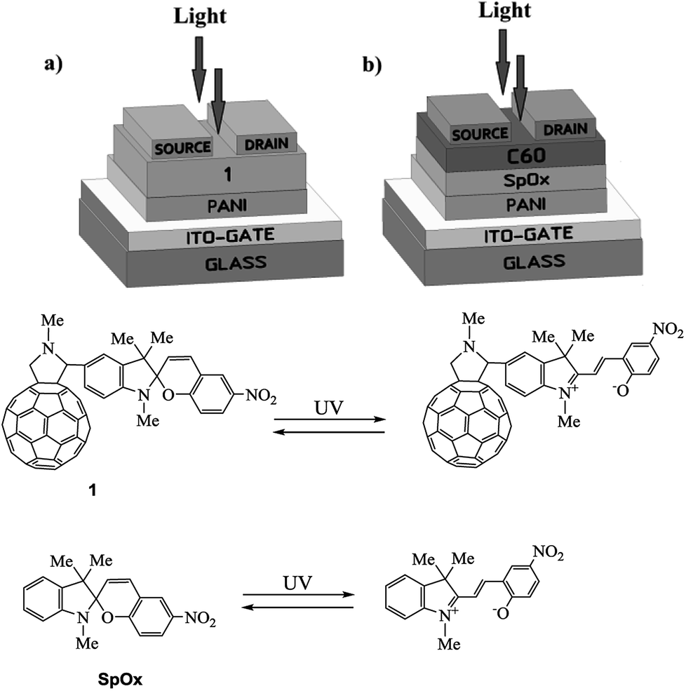 | ||
| Fig. 1 Structures of photocontrolled OFETs presented in this study. The UV light-induced reversible isomerization of the spiropyran moiety to the merocyanine form within hybrid molecule 1 in OFET (a) and model spiropyran SpOx to merocyanine in OFET (b) is shown below. | ||
The study of the current–voltage characteristics of the fabricated transistors has shown that, in the absence of irradiation, the currents in the phototransistors are less than 1 nA or have the same order of magnitude. Under UV light irradiation (350 nm), in the field of the transistor gap the drain-to-source current increases by three orders of magnitude for both devices. Thus, the current ratio Ion/Ioff is about 1000. Fig. 2 show the transfer and output characteristics of OFETs. In all cases, the currents for structures with a hybrid molecule 1 layer exceeded the values of current for structures with separate layers by several tenths of microamperes (μA). An increase in currents in the created OFETs is observed under a positive gate voltage, which corresponds to the electronic conductivity type of the OFET transport channel. Dependencies are nonlinear. The output characteristics show the absence of the saturation regions. Higher voltages (VDS) are most likely required to achieve them.
 | ||
| Fig. 2 (a) Transfer and (b) output characteristics of OFETs based on hybrid (solid lines) and separate (dashed lines) active layers. | ||
A possible explanation for the pronounced increase in the current through the transistor is the zwitter-ion effect, which leads to a sharp increase in the dipole moment of the spiropyran molecule (from 6.4 D to 13.9 D)19 upon UV irradiation. Voltage application to the transistor gate induces predominant orientation of polarized molecules, which in turn sharply increases the field effect in the transistor.
The charge carrier mobilities of the OFET active layer μ were found from eqn (1):
| IDS = (W/L)μC(VG − Vth)VDS, | (1) |
The calculated carrier mobilities were 1.8 cm2 V−1 s−1 and 2.3 cm2 V−1 s−1 for the “separately deposited” active layer and for the hybrid active layer, respectively. The obtained values are comparable with data3,20 determined recently for films of fullerenes and fullerene derivatives used in organic electronics.
A typical IDS relaxation kinetics for OFETs upon light switching on and off (with a power of ∼150 W cm−2) with VDS = 3 V and Vg = 3 V is shown in Fig. 3. It can be seen that the output current depends on the irradiation time of the conducting channel, with the maximum values being attained within 12 s after the light is switched on. The initial state of transistors is attained within 1–2 s after the activating light is switched off.
 | ||
| Fig. 3 Kinetics of the increase and decrease in the currents IDS for OFETs based on double layers and hybrid layer 1 on switching on and off of ultraviolet light (150 W, 350 nm) for VDS = 3 V and VG = 3 V. | ||
It can be seen in Fig. 3 that the current is higher in the OFET based on the hybrid compound than in the multilayer device, which is attributable to the fact that in the latter case, fewer photons reach the photochromic layer as a result of absorption in the organic semiconductor film.
The response of the transistors to external influence was evaluated using characteristics such as photosensitivity (P) and responsivity (R). The photosensitivity P is defined as the photogenerated to dark current ratio and can be found as
| P = Iph/Idark = (Iillum − Idark)/Idark | (2) |
On the other hand, the R value can be defined as the ratio of the generated photocurrent to the incident optical power (Popt); hence, the responsivity R can be calculated by the following equation:
| R = Iph/Popt = (Iillum − Idark)/Eopta | (3) |
The photosensitivities estimated by relation (3) were 1800 and 1400 for the phototransistor based on fullerene C60 and spiropyran hybrid film and the phototransistor fabricated with separate film deposition, respectively. The responsivity calculation yielded the values of 180 μA W−1 for the hybrid transistor and 140 μA W−1 for the separate-layer transistor. The calculations assumed that the area of the device accessible to the incident light was not more than 5 × 10⁻³ cm2. Then, considering the emitter characteristics which provide the incident power density of approximately 2 W cm−2, we obtain the overall radiation power on the phototransistor to be about 10 mW.
Experiment and the literature data show that the best results are achieved in transistors with a multilayer structure (Fig. 1b) having layers thickness (semiconductor (C60) and photochromic) of 200 nm each. Upon fabrication of the device based on hybrid compound 1 (Fig. 1a), the thickness of the combined semiconductor and photochromic layers was done 300 nm (see ESI†). At the same time, it was found that the increase in the thickness of the photochromic layer in the device (Fig. 1b) leads to a decrease in the output current due to a decrease in the influence of the gate field on the carrier concentration in the transport layer. A decrease in the thickness of this layer leads to a weakening of the zwitterion effect and, as a consequence, a weakening of the output current.
In view of the potential applications of these transistors as memory cells, special attention in the development of these devices is paid to their stability and reliability. It is shown in Fig. 4 that the transistors that we fabricated can repeatedly switch between on- and off-states with their electrical characteristics being retained.
 | ||
| Fig. 4 Cycling stability of the devices switched 40 times between two arbitrarily selected electrical states: (a) hybrid layer; (b) separate layers. | ||
It should be noted that structures fabricated from pyrrolidinofullerene 1 proved to be stable to UV radiation. The films of separately deposited C60 and SpOx degraded during operation thus destroying contact Al films. The studies of transistors described above indicate that transistors based on the hybrid molecule were superior in all of the measured characteristics; furthermore, their fabrication is more feasible.
Conclusions
Thus, OFETs with active layers based on the fullerene C60 and spiropyran hybrid molecule studied in this work possess high carrier mobility in the channel and relatively high responsivity and photosensitivity. The main advantage of such hybrid structures is their high stability, which was confirmed during high-speed tests with multiple switching (ON and OFF) that reflect the performance of a device. The results of the studies are of practical value for the design of memory cells with optical recording, optrons, and photosensors. An advantage of these devices is that their fabrication technique is compatible with the modern organic printed electronic techniques. All measurements were carried out under normal conditions – in the air, which is the advantage of the transistor structures studied, as compared with most experimental structures based on other compounds, when you have to work in inert gas or dry nitrogen using glove box. Further studies of the transport, generation, and relaxation of photoinduced charge carriers in these structures are required for optimization of their performance characteristics.Conflicts of interest
There are no conflicts to declare.Acknowledgements
This work was supported by the Russian Foundation for Basic Research (N 18-33-20027) and Grants of the RF President (MK-3058.2018.3 and Sci. Sh.-5240.2018.3). The structural studies were performed at the Center for Collective Use “Agidel” at the Institute of Petrochemistry and Catalysis of the RAS.Notes and references
- M. E. Gemayel, K. Borjesson, M. Herder, D. T. Duong, J. A. Hutchison, C. Ruzie, G. Schweicher, A. Salleo, Y. Geerts, S. Hecht, E. Orgiu and P. Samori, Nat. Commun, 2015, 1, 6330 CrossRef PubMed.
- L.-N. Fu, B. Leng, Y.-S. Li and X.-K. Gao, Chin. Chem. Lett., 2016, 27, 1319 CrossRef CAS.
- Y. Zhang, I. Murtaza and H. Meng, J. Mater. Chem. C, 2018, 6, 3514 RSC.
- A. Pivrikas, N. S. Sariciftci, G. Juska and R. Osterbacka, Prog. Photovoltaics, 2007, 15, 677 CAS.
- F. Garnier, A. Yassar, R. Hajlaoui, G. Horowitz, F. Deloffre, B. Servet, S. Ries and P. Alnot, J. Am. Chem. Soc., 1993, 115, 8716 CrossRef CAS.
- A. R. Tuktarov, A. A. Khuzin and U. M. Dzhemilev, Russ. Chem. Rev., 2017, 86, 474 CrossRef CAS.
- K. Borjesson, M. Herder, L. Grubert, D. T. Duong, A. Salleo, S. Hecht, E. Orgiu and P. Samori, J. Mater. Chem. C, 2015, 3, 4156 RSC.
- L. A. Frolova, A. A. Rezvanova, B. S. Lukyanov, N. A. Sanina, P. A. Troshin and S. M. Aldoshin, J. Mater. Chem. C, 2015, 3, 11675 RSC.
- L. A. Frolova, P. A. Troshin, D. K. Susarova, A. V. Kulikov, N. A. Sanina and S. M. Aldoshin, Chem. Commun., 2015, 51, 6130 RSC.
- L. A. Frolova, A. A. Rezvanova, V. Z. Shirinian, A. G. Lvov, A. V. Kulikov, M. M. Krayushkin and P. A. Troshin, Adv. Electron. Mater., 2016, 2, 1500219 CrossRef.
- A. A. Rezvanova, L. A. Frolova and P. A. Troshin, Mendeleev Commun., 2016, 26, 26 CrossRef CAS.
- E. Orgiu and P. Samori, Adv. Mater., 2014, 26, 1827 CrossRef CAS PubMed.
- A. R. Tuktarov, A. A. Khuzin, A. R. Tulyabaev, O. V. Venidictova, T. M. Valova, V. A. Barachevsky, L. M. Khalilov and U. M. Dzhemilev, RSC Adv., 2016, 6, 71151 RSC.
- V. A. Pomogaev, V. A. Barachevsky, A. R. Tuktarov, P. V. Avramov and V. Ya. Artyukhov, J. Phys. Chem. A, 2018, 122, 505 CrossRef CAS PubMed.
- A. R. Tuktarov, A. A. Khuzin, L. M. Khalilov, A. R. Tulyabaev, A. R. Akhmetov and U. M. Dzhemilev, Mendeleev Commun., 2015, 25, 470 CrossRef CAS.
- A. R. Tuktarov, A. A. Khuzin, A. R. Akhmetov, V. A. Barachevsky, O. V. Venidiktova and U. M. Dzhemilev, Tetrahedron Lett., 2015, 56, 7154 CrossRef CAS.
- A. R. Tuktarov, A. A. Khuzin, A. R. Akhmetov, L. M. Khalilov, A. R. Tulyabaev, V. A. Barachevsky, O. V. Venidiktova and U. M. Dzhemilev, Mendeleev Commun., 2016, 26, 143 CrossRef CAS.
- A. R. Tuktarov, A. R. Akhmetov, A. A. Khuzin, O. V. Venidiktova, V. A. Barachevskii and U. M. Dzhemilev, Russ. J. Org. Chem., 2017, 53, 891 CrossRef CAS.
- Y. Ishiguro, R. Hayakawa, T. Chikyow and Y. Wakayama, J. Mater. Chem. C, 2013, 1, 3012 RSC.
- J. M. Ball, R. K. M. Bouwer, F. B. Kooistra, J. M. Frost, Y. Qi, E. B. Domingo, J. Smith, D. M. de Leeuw, J. C. Hummelen, J. Nelson, A. Kahn and N. Stin, J. Appl. Phys., 2011, 110, 014506 CrossRef.
Footnote |
| † Electronic supplementary information (ESI) available. See DOI: 10.1039/c9ra00939f |
| This journal is © The Royal Society of Chemistry 2019 |