
 Open Access Article
 This Open Access Article is licensed under a Creative Commons Attribution-Non Commercial 3.0 Unported Licence
Highly bright perovskite light-emitting diodes based on quasi-2D perovskite film through synergetic solvent engineering
Huanxin Yueab,
Dandan Song*ab,
Suling Zhao ab,
Zheng Xuab,
Bo Qiaoab,
Songquan Wuab and
Juan Mengab
ab,
Zheng Xuab,
Bo Qiaoab,
Songquan Wuab and
Juan Mengab
aKey Laboratory of Luminescence and Optical Information, Ministry of Education, Beijing Jiaotong University, Beijing 100044, China. E-mail: ddsong@bjtu.edu.cn
bInstitute of Optoelectronic Technology, Beijing Jiaotong University, Beijing 100044, China
First published on 14th March 2019
Abstract
Recently, quasi-two dimensional (2D) perovskites have attracted great interest as they can be facilely fabricated and yield high photoluminescence quantum yield. However, the luminance and the efficiency of perovskite light-emitting diodes (PeLEDs) based on quasi-2D perovskites are limited by the carrier transport and the crystallization properties of the quasi-2D perovskite films. Herein, a synergetic solvent engineering approach is proposed to improve the crystallinity and the carrier transport by optimizing the film morphology of the quasi-2D perovskite films. Consequently, the maximum luminance of green PeLEDs based on quasi-2D PEA2 (MAPbBr3)2PbBr4 perovskite is dramatically enhanced from 4000 cd m−2 to 18![[thin space (1/6-em)]](https://www.rsc.org/images/entities/char_2009.gif) 000 cd m−2 and the current efficiency increases from 3.40 cd A−1 to 8.74 cd A−1. This work provides a promising way to control the morphology and the crystallinity properties of quasi-2D perovskite films for high-performance optoelectronic devices.
000 cd m−2 and the current efficiency increases from 3.40 cd A−1 to 8.74 cd A−1. This work provides a promising way to control the morphology and the crystallinity properties of quasi-2D perovskite films for high-performance optoelectronic devices.
Introduction
Organic–inorganic halide perovskites have attracted much attention due to their high color purity and low-cost solution processability. In 2014, the first strong room-temperature electroluminescence in perovskite light-emitting diodes (PeLEDs) was demonstrated by Tan et al.1 Subsequently, various research methods have been used to improve the efficiency of PeLEDs.2–9 Up to now, a maximum external quantum efficiency (EQE) of up to 20.3% was achieved based on three-dimensional (3D) PeLEDs.10 Meanwhile, quasi-two-dimensional (quasi-2D) green PeLEDs, in which the quasi-2D perovskite has the molecular formula PEA2(FAPbBr3)n−1 PbBr4 (with n = 3), with current efficiency (CE) of 62.4 cd A−1 and EQE of 14.36% were achieved, which is the highest current efficiency for quasi-2D PeLEDs reported so far.11 The quasi-2D perovskites possess better stability potential than their conventional 3D counterparts, and thus are potential candidates for highly efficient and stable luminescent materials.11–15 Though the PeLEDs based on quasi-2D perovskites possess high efficiency, the luminance is typically low9,13,16 (<10000 cd m−2 for the most efficient PeLEDs based on quasi-2D perovskites11). The low luminance can be ascribed to the severe carrier recombination and inefficient carrier transport inside the solution processed thin films of quasi-2D perovskites. The grain size of the quasi-2D perovskites is required to be small to confine the carriers (excitons), and hence, the carrier recombination inside the grains and near the grain boundaries are much obvious. Meanwhile, due to the small grain size and the insulate nature of the organic spacer cations, carrier transport is limited in the perovskite film.17 Therefore, in order to enhance the device luminance, it is critical to control the crystallization process of the quasi-2D perovskite grains during film fabrication, aiming to minimize the carrier recombination and simultaneously enhances the carrier transport governed by the crystallization quality and grain size of the quasi-2D perovskite.
In terms of controlling the crystallinity of the perovskite film, various approaches have been developed, among which the solvent engineering is proved to be quite efficient.18–27 In the field of 3D perovskite materials and their application in solar cells, it is well demonstrated that both the solvent for dissolving the precursors of the perovskite material (abbreviated as the dissolving solvent hereafter) and the anti-solvent dipped during the spin-coating process (abbreviated as the anti-solvent hereafter) greatly affect the crystallization process of the perovskite grains. For example, it is shown that the dissolving solvent dimethyl sulfoxide (DMSO) impedes the crystallization of PbI2 and MAPbI3 leading to the formation of much smaller perovskite grains compared with the solvent dimethyl form amide (DMF).28 To adjust the crystallization process through utilizing the differences of the dissolving solvents, mixed dissolving solvents are also proposed. For example, a recent study shows that DMF/DMSO mixed dissolving solvents can obtain high quality perovskite films with uniform morphology, enhanced crystallinity, and efficient carrier transport, leading to the enhanced power conversion efficiency (PCE) of the perovskite solar cells (PSCs) by 10%.29 Besides, the anti-solvent chlorobenzene (CB) can greatly enhances the crystallization of the perovskite, favoring the formation of large grains and dense film, which becomes a commonly used anti-solvent in both PSCs and PeLEDs.30,31 In PeLEDs, DMSO is typically used as the dissolving solvent to enable the formation of small grains and CB is also used as anti-solvent to prepare dense film. Attempts to modify the solvent and the anti-solvent are also made to improve the device performance of the PeLEDs. Solvent engineering, especially simultaneously modifying the dissolving solvent and the anti-solvent, in preparing the perovskite films for highly bright and efficient PeLEDs is still essential.
In this work, a strategy to control the crystallization process and the resultant properties of the quasi-2D perovskite film is demonstrated by simultaneously modifying the dissolving solvent and the anti-solvent. The quasi-2D PeLEDs based on PEA2 (MAPbBr3)n−1 PbBr4 with n = 3 composition are used as the emitting layer. The dissolving solvent, DMSO, and the anti-solvent, CB, are simultaneously modified by DMF to control the crystallization of the perovskite film and the resultant performance. As a result, the maximum luminance of green PeLEDs is dramatically enhanced from 4000 cd m−2 to 18000 cd m−2 and the current efficiency increase from 3.40 cd A−1 to 8.74 cd A−1. Our methods pave the way for further development of high-quality quasi-2D perovskite films for efficient PeLEDs devices.
Experimental
The PeLEDs have the architecture of ITO/PEDOT:PSS/perovskite/TPBi/LiF/Al. The pre-cleaned indium-tin oxide (ITO) glass substrates were treated using UV–ozone for 10 min. The poly(3,4-ethylenedioxythiophene):poly (styrene sulfonate) (PEDOT:PSS) as hole transport layer (HTL) was spin-coated onto the ITO substrates at 2000 rpm for 40 s, then they were dried at 150 °C for 10 min in air. Then the substrates were transferred into glove box filled with nitrogen. The perovskite precursor solution was prepared by dissolving lead bromine (PbBr2), methylammonium bromine (MABr), phenylethyl ammonium bromide (PEABr) and methylammonium chloride (MACl) (in a molar ratio of 0.6:0.4:0.4:0.06) in different volume ratio of DMF and DMSO mixed solvents with a concentration of 0.4 M. Then perovskite solution was spin-coated onto PEDOT:PSS at 3000 rpm for 120 s, and during the spin-coating stage, 200 μl of CB or CB + 10 vol% DMF anti-solvent was dipped, followed by annealing on a hot plate at 90 °C for 30 min. Finally, the stacks of TPBi (40 nm)/LiF (1 nm)/Al (100 nm) were thermally deposited in sequence in a vacuum chamber at a base pressure < 5 × 10⁻⁴ Pa through a shadow mask. The device area is defined by the overlap of the Al and ITO electrodes which is 9 mm2.
ITO glasses with a sheet resistance of 15 Ω sq−1 were purchased from Huanan Xiang cheng Technology Co., Ltd. PEDOT:PSS (AI 4083) was purchased from Clevios. PbBr2, MACl and 2,2′,2′′-(1,3,5-benzinetriyl)-tris(1-phenyl-1-H-benzimidazole) (TPBi) were purchased from Xi'an Polymer Light Technology Corp. MABr and PEABr were purchased from Dyesol.
Scanning electron microscope (SEM) measurements were performed by a Hitachi 4800. X-ray diffraction (XRD) patterns were collected with a D/max 2200 V X-ray powder diffractometer with Cu Kα radiation (λ = 1.540 A). The current density–voltage–luminance (J–V–L) characteristics and electroluminescence (EL) spectra of the PeLEDs were measured on a Keithley 2400 source meter combined with a Newport 1830-R optical power meters equipped with 918D calibrated photodiode. The steady-state photoluminescence (PL) emission spectra were recorded on a Hitachi F4500 fluorescence spectrophotometer with a Xe lamp coupled to a monochromator. All measurements were carried out at room temperature under ambient atmosphere.
Results and discussions
Fig. 1 shows a schematic illustration for the effects of the solvents on the crystallization processes and the resultant morphology of the quasi-2D perovskite films. DMSO yields a much slower crystallization process (less nuclei formation before dipping the anti-solvent) than DMF solvent (more nuclei formation before dipping the anti-solvent) due to its large polarity for dissolving the perovskite precursors and high boiling temperature. Therefore, the crystallization process can be tuned by modifying the ratio of DMSO/DMF in the precursor solution. CB excludes the dissolving solvent and thus accelerates the crystallization of the perovskite film, leading to the formation of large grains through the fast inhomogeneous growth from the perovskite nuclei. Introducing DMF in CB dilutes CB in the precursor solvent and will lower the crystallization process. Hence, the crystallization of the perovskite film is adjusted by simultaneously adjusting the dissolving and anti-solvents.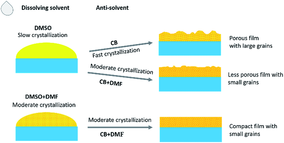 | ||
| Fig. 1 Schematic illustration for the effects of the solvents on the crystallization processes and the resultant morphology of the quasi-2D perovskite films. | ||
The morphology features of the perovskite films employing different solvent recipes were characterized by SEM, and the images are shown in Fig. 2. The standard film, fabricated from pure DMSO solvent and pure CB anti-solvent, shows a porous surface with grains smaller than 100 nm (Fig. 2a). With the addition of DMF (10 vol%) in CB anti-solvent, the perovskite film (Fig. 2b) shows less porous surface and obviously smaller grains compared to the standard perovskite film. These changes can be ascribed to the modification in the crystallization process of the perovskite film by DMF, which lowers the crystallization rate and favors the formation of less porous film with smaller grains. By adjusting the ratio of DMF in the DMSO dissolving solvent, it can be seen that the perovskite film becomes more and more compact with increasing the DMF content (Fig. 2c–f). The addition of DMF in DMSO enhances the initial nuclei formation in the perovskite film, and hence, in the grain growth process by dipping the anti-solvent, the grains are more compactly grown.
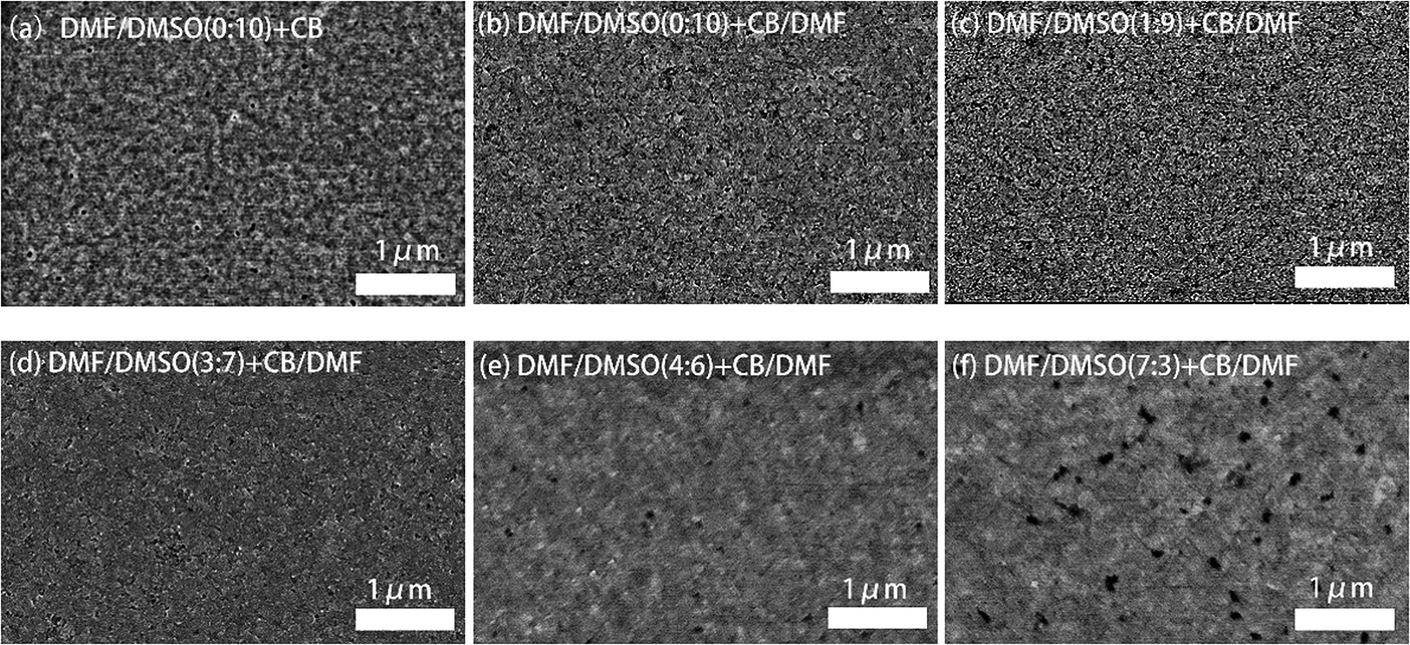 | ||
| Fig. 2 SEM images of quasi-2D perovskite films fabricated from different solvent recipes. (a) DMF/DMSO (0:10) + CB, (b) DMF/DMSO (0:10) + CB/DMF, (c) DMF/DMSO (1:9) + CB/DMF, (d) DMF/DMSO (3:7) + CB, (e) DMF/DMSO (4:6) + CB, (f) DMF/DMSO (7:3) + CB/DMF. All of the ratios are volume ratios. | ||
The crystallinity of the perovskite films was characterized by XRD measurement, and the XRD patterns are shown in Fig. 3a. Four characteristic peaks at 14.95°, 21.38°, 30.20°and 35.26°, assigned to (100), (110), (200) and (210) crystal planes of the quasi-2D perovskite respectively, can be clearly observed in all of the perovskite films. Previous report has proved that all quasi-2D perovskite films contain both 3D and quasi-2D perovskite crystals by conducting grazing-incidence X-ray diffraction (GI-XRD).13 All the XRD patterns of our perovskite films show the diffraction peaks around 14.95°, which is attributed to the diffraction peak of (100) plane of the 3D perovskite MAPbBr3. These observations are similar to the conditions of perovskite films in previous reports.16,32 The full width at half maximum (FWHM) of the main diffraction peak (14.95°) increase from 0.66° to 0.81° by introducing DMF in dissolving solvent, revealing the decreased grain size in these films, which is consistent with the SEM observations. The relative diffraction intensity is much stronger in the perovskite films with DMF in both dissolving solvent and anti-solvent, partially reflecting the enhanced crystallinity in these films.
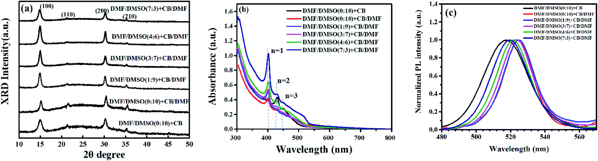 | ||
| Fig. 3 (a) X-ray diffraction patterns, (b) the absorption spectra, and (c) the PL spectra of perovskite films prepared by using different anti-solvents and dissolving solvents. | ||
The UV-vis absorbance and PL spectra of the quasi-2D perovskite films were also analyzed and are shown in Fig. 3b and c. As shown in Fig. 3b, the absorption edges are similar for all the perovskite films, which are around 530 nm. Three obvious absorption peaks appear around 400 nm, 431 nm and 450 nm, which also implies that the films consist of quasi-2D perovskite crystals.13 The PL spectra of the corresponding quasi-2D perovskite films exhibit red-shift by introducing DMF in anti-solvent. It is attributed to the decreased crystalline domain sizes of quasi-2D perovskite films with more defect states at grain boundaries. The grain size is relatively large and do not cause quantum confinement effects. Huang et al. have reported that the emission from the spontaneous radiative recombination between the trap states, which shows a redshifted emission peak compared with that from the band edge transition.33 Fig. 3c displays that the PL spectra is blue-shift with the rate of DMF/DMSO increasing, which is due to the reduced defect states by the enhanced crystallinity through introducing DMF in dissolving solvent.
The enhanced crystallinity and the compact film with smaller grains formed by introducing DMF in anti-solvent solely or also in dissolving solvent is benefit for increasing the carrier transport and confining the excitons inside the grains, which will lead to high performance PeLEDs. The schematic structure of the PeLEDs is shown in Fig. 4a, which employs PEDOT:PSS as the HTL and TPBi as the ETL. The corresponding energy level diagram is also shown in Fig. 4b. The EL spectra of the PeLEDs are shown in Fig. 4c. It is clear that the change of the peak locations of the EL spectra is similar to that of the PL spectra, as also summarized in Table 1. The standard PeLEDs (without solvent engineering for preparing perovskite film, i.e., with pristine DMSO as the dissolving solvent and pristine CB as the anti-solvent) shows the EL peak at 514 nm while the addition of DMF in CB anti-solvent shifts the EL peak to the long wavelength. The addition of DMF in DMSO makes the EL peak blue-shifting. These EL emission are all from the perovskite films, illustrating that the emission is confined in the perovskite emission layer (EML).
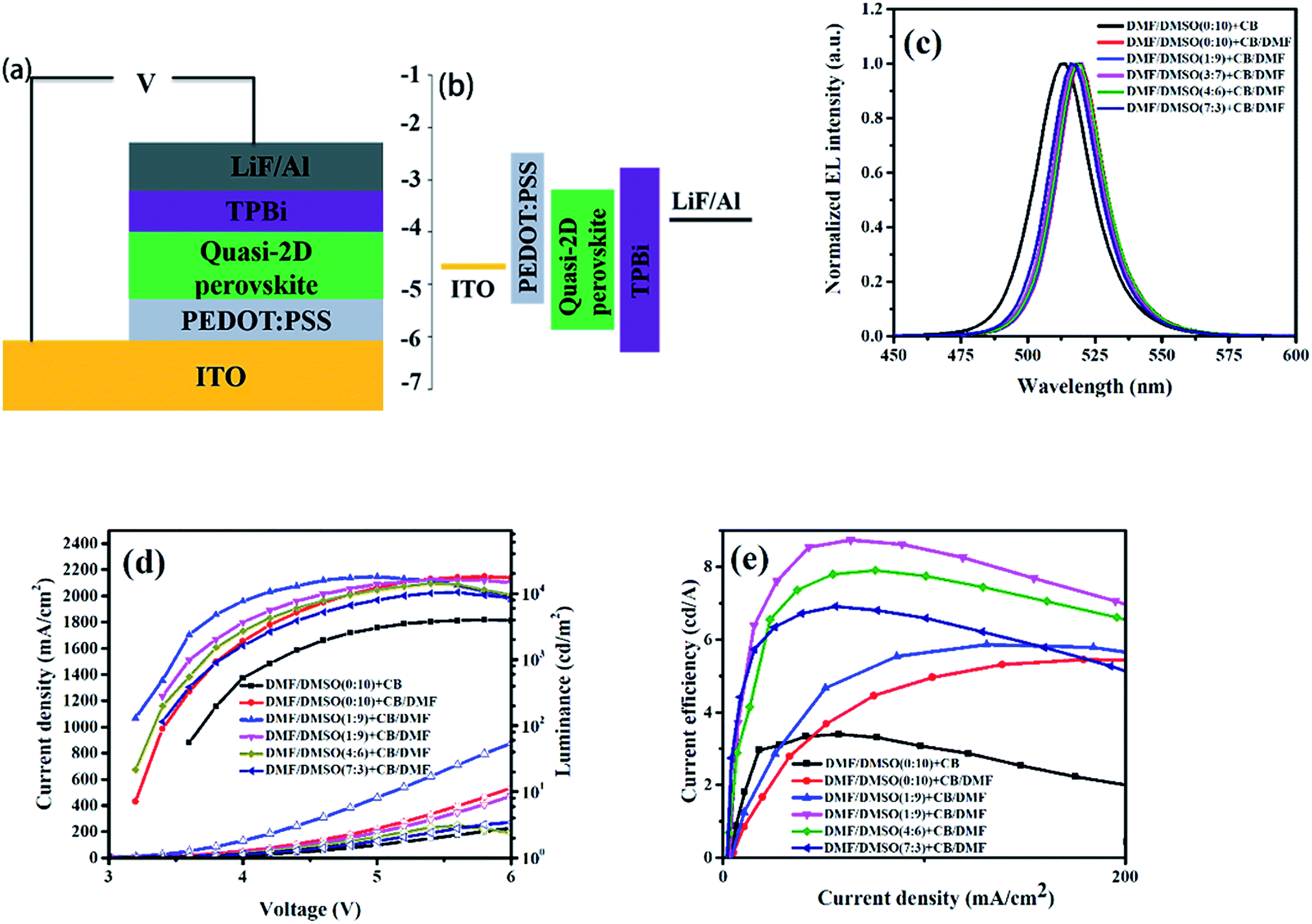 | ||
| Fig. 4 Perovskite light-emitting diodes structure and electroluminescence. (a) Device architecture employed in this work, (b) band alignment of each function layer in the devices, (c) typical electroluminescence spectra of different perovskite LEDs under 5 voltage bias, (d) device performance of perovskite LEDs with different anti-solvent J–V–L, (e) CE versus voltage (CE–V) curves. | ||
| Solvent recipe | PL peaks | EL peaks | Lmax (cd m−2) | CEmax (mA cm−2) |
|---|---|---|---|---|
| DMF/DMSO (0:10) + CB |
517 | 514 | 4000 | 3.40 |
| DMF/DMSO (0:10) + CB/DMF |
524 | 520 | 18000 |
5.45 |
| DMF/DMSO (1:9) + CB/DMF |
525 | 520 | 18000 |
5.87 |
| DMF/DMSO (3:7) + CB/DMF |
523 | 518 | 16200 |
8.74 |
| DMF/DMSO (4:6) + CB/DMF |
522 | 518 | 14214 |
7.79 |
| DMF/DMSO (7:3) + CB/DMF |
520 | 516 | 10502 |
6.72 |
Fig. 4d and e shows the J–V–L curves and the current efficiency versus current density (CE–J) curves, respectively, of the PeLEDs fabricated from different solvent recipes. The detailed device parameters are summarized in Table 1. It can be seen that the standard PeLED shows a maximum luminance (Lmax) of 4005 cd m−2 and a maximum CE (CEmax) of 3.40 cd A−1. It shall be mentioned that other preparation parameters of the perovskite film including the thickness, the precursor concentration/composition, the dipping procedure of the anti-solvent and the post-annealing temperature/time were already optimized in the standard PeLEDs. By introducing DMF in CB anti-solvent, the PeLEDs shows obviously increased current density, luminance and CE, leading to a Lmax of 18000 cd m−2 and a CEmax of 5.45 cd A−1. The luminance is greatly improved by solvent engineering method, which value is higher than the typically reported values from PeLEDs based on quasi-2D perovskite (around @ cd m−2). The current density, the luminance and the CE of the PeLEDs are determined by the following equations
| L ∝ Rnp ∝ RJeJh |
where Je (Jh),
 n(p) and R represent for the electron (hole) current density, the leaked electron (hole) current, the electron (hole) concentration in the EML and the bimolecular radiative recombination rate, respectively. Hence, the simultaneously increased current density and luminance by introducing DMF in CB anti-solvent implies higher electron and/or hole current in the corresponding PeLEDs. As the injection energy barrier has not been changed, the increased carrier current indicates the enhanced carrier transport inside the perovskite film, which can be well explained by the reduced porosity by introducing DMF in CB anti-solvent (Fig. 1). Moreover, the increased CE can also be partially ascribed to the reduced porosity, which reduces the leakage current and thus favors high CE. Meanwhile, the exciton confining, enabled by the smaller grains in the perovskite film fabricated with DMF in CB anti-solvent, is beneficial to increase R, which may also partially explain the increased CE of the PeLEDs fabricated with DMF in CB anti-solvent (compared to the standard PeLEDs).
By introducing DMF in DMSO solvent, the CE is further increased. As can be seen from Fig. 4d and e with increasing the DMF/DMSO ratio, the current density and luminance firstly increases with the addition of DMF in DMSO solvent, and then decreases. The CE displays the similar trend, which achieves the best for the condition of DMF/DMSO with a ratio of 3:7 (vol:vol). These trends can be explained by the trade-offs between the carrier transport and the carrier injection induced by the morphology and crystallinity of the perovskite film. The improved compact feature and the enhanced crystallinity of the perovskite films with increasing the DMF/DMSO ratio enhance the carrier transport and reduce the leakage current, leading to increased current density/luminance/CE; but meanwhile, they also lead to reduced carrier injection from the ETL to the perovskite due to the minimized carrier injection interface by the compact film, leading to lowered current density/luminance/CE.
The highest CE obtained from the PeLEDs with solvent engineering is 8.74 cd A−1, which is more than 2.5 times higher than that of the standard PeLEDs without solvent engineering. The maximum luminance obtained the PeLEDs with solvent engineering is 18000 cd m−2, which is 4.5 times higher than that of the standard PeLEDs. These improvements demonstrate the efficacy of the synergetic solvent engineering in optimize the device performance. In addition, the efficiency roll-off of the PeLEDs is also suppressed by solvent engineering, which enables the PeLEDs working at high luminance with much higher efficiency.
Conclusion
In conclusion, we propose the synergistic solvent engineering strategy, i.e., simultaneously modifying the dissolving solvent and the anti-solvent, to improve the crystallinity and the carrier transport of the quasi-2D perovskite films for bright PeLEDs. The PeLEDs based on the quasi-2D perovskite films with solvent engineering exhibit a high luminance of 18000 cd m−2 and a CE of 8.74 cd A−1, which are 4.5 and 2.5 times higher than the standard PeLEDs. This work demonstrates the efficacy and the principle of the synergistic solvent engineering strategy in optimizing the device performance, and also provides a promising way to control the morphology and the crystallinity properties of quasi-2D perovskite films for high-performance optoelectronic devices.
Conflicts of interest
There are no conflicts to declare.Acknowledgements
The authors express their thanks to the Fundamental Research Funds for the Central Universities with Grant No. 2017RC015; the National Natural Science Foundation of China under Grant No. 61775013 and 61575019; and the fund support from Shenzhen China Star Optoelectronics Technology Co., Ltd.Notes and references
- Z. K. Tan, R. S. Moghaddam, M. L. Lai, P. Docampo, R. Higler, F. Deschler, M. Price, A. Sadhanala, L. M. Pazos, D. Credgington, F. Hanusch, T. Bein, H. J. Snaith and R. H. Friend, Nat. Nanotechnol., 2014, 9, 687–692 CrossRef CAS PubMed.
- H. Cho, S. H. Jeong, M. H. Park, Y. H. Kim, C. Wolf, C. L. Lee and S. H. Im, Science, 2015, 350, 1222–1225 CrossRef CAS PubMed.
- J. Wang, N. Wang, Y. Jin, J. Si, Z. K. Tan, H. Du, L. Cheng, X. Dai, S. Bai, H. He, Z. Ye, M. L. Lai, R. H. Friend and W. Huang, Adv. Mater., 2015, 27, 2311–2316 CrossRef CAS PubMed.
- Z. Xiao, R. A. Kerner, L. Zhao, N. L. Tran, K. M. Lee, T.-W. Koh, G. D. Scholes and B. P. Rand, Nat. Photonics, 2017, 11, 108–115 CrossRef CAS.
- L. Zhao, Y. W. Yeh, N. L. Tran, F. Wu, Z. Xiao, R. A. Kerner, Y. L. Lin, G. D. Scholes, N. Yao and B. P. Rand, ACS Nano, 2017, 11, 3957–3964 CrossRef CAS PubMed.
- J. C. Yu, D. B. Kim, E. D. Jung, B. R. Lee and M. H. Song, Nanoscale, 2016, 8, 7036–7042 RSC.
- X. Zhao, B. Zhang, R. Zhao, B. Yao, X. Liu, J. Liu and Z. Xie, J. Phys. Chem. Lett., 2016, 7, 4259–4266 CrossRef CAS PubMed.
- P. Chen, Z. Xiong, X. Wu, M. Shao, X. Ma, Z. H. Xiong and C. Gao, J. Phys. Chem. Lett., 2017, 8, 1810–1818 CrossRef CAS PubMed.
- S. Kumar, J. Jagielski, N. Kallikounis, Y. H. Kim, C. Wolf, F. Jenny, T. Tian, C. J. Hofer, Y. C. Chiu, W. J. Stark, T. W. Lee and C. J. Shih, Nano Lett., 2017, 17, 5277–5284 CrossRef CAS PubMed.
- K. Lin, J. Xing, L. N. Quan, F. P. G. de Arquer, X. Gong, J. Lu, L. Xie, W. Zhao, D. Zhang, C. Yan, W. Li, X. Liu, Y. Lu, J. Kirman, E. H. Sargent, Q. Xiong and Z. Wei, Nature, 2018, 562, 245–248 CrossRef CAS PubMed.
- X. Yang, X. Zhang, J. Deng, Z. Chu, Q. Jiang, J. Meng, P. Wang, L. Zhang, Z. Yin and J. You, Nat. Commun., 2018, 9, 570 CrossRef PubMed.
- M. Yuan, L. N. Quan, R. Comin, G. Walters, R. Sabatini, O. Voznyy, S. Hoogland, Y. Zhao, E. M. Beauregard, P. Kanjanaboos, Z. Lu, D. H. Kim and E. H. Sargent, Nat. Nanotechnol., 2016, 11, 872–877 CrossRef CAS PubMed.
- J. Byun, H. Cho, C. Wolf, M. Jang, A. Sadhanala, R. H. Friend, H. Yang and T. W. Lee, Adv. Mater., 2016, 28, 7515–7520 CrossRef CAS PubMed.
- H. Cho, Y. H. Kim, C. Wolf, H. D. Lee and T. W. Lee, Adv. Mater., 2018, 30, e1704587 CrossRef PubMed.
- Y. Chen, Y. Sun, J. Peng, J. Tang, K. Zheng and Z. Liang, Adv. Mater., 2018, 30 Search PubMed.
- G. Jia, Z. J. Shi, Y. D. Xia, Q. Wei, Y. H. Chen, G. C. Xing and W. Huang, Opt. Express, 2018, 26, A66–A74 CrossRef CAS PubMed.
- Y. H. Kim, J. S. Kim and T. W. Lee, Adv. Mater., 2018, e1804595, DOI:10.1002/adma.201804595.
- B. Jiao, X. Zhu, W. Wu, H. Dong, B. Xia, J. Xi, T. Lei, X. Hou and Z. Wu, Nanoscale, 2016, 8, 11084–11090 RSC.
- J. C. Yu, D. W. Kim, D. B. Kim, E. D. Jung, K. S. Lee, S. Lee, D. D. Nuzzo, J. S. Kim and M. H. Song, Nanoscale, 2017, 9, 2088–2094 RSC.
- M.-H. Park, S.-H. Jeong, H.-K. Seo, C. Wolf, Y.-H. Kim, H. Kim, J. Byun, J. S. Kim, H. Cho and T.-W. Lee, Nano Energy, 2017, 42, 157–165 CrossRef CAS.
- Y. Zhu, X. Zhao, B. Zhang, B. Yao, Z. Li, Y. Qu and Z. Xie, Org. Electron., 2018, 55, 35–41 CrossRef CAS.
- R. Naphade, B. Zhao, J. M. Richter, E. Booker, S. Krishnamurthy, R. H. Friend, A. Sadhanala and S. Ogale, Adv. Mater. Interfaces, 2017, 4, 1700562 CrossRef.
- S. Lee, J. H. Park, Y. S. Nam, B. R. Lee, B. Zhao, D. Di Nuzzo, E. D. Jung, H. Jeon, J. Y. Kim, H. Y. Jeong, R. H. Friend and M. H. Song, ACS Nano, 2018, 12, 3417–3423 CrossRef CAS PubMed.
- X. Qin, H. Dong and W. Hu, Sci. China Mater., 2015, 58, 186–191 CrossRef CAS.
- W. Q. Wu, D. Chen, W. A. McMaster, Y. B. Cheng and R. A. Caruso, ACS Appl. Mater. Interfaces, 2017, 9, 31959–31967 CrossRef CAS PubMed.
- W.-Q. Wu, D. Chen, R. A. Caruso and Y.-B. Cheng, J. Mater. Chem. A, 2017, 5, 10092–10109 RSC.
- W.-Q. Wu and L. Wang, J. Mater. Chem. A, 2019, 7, 932–939 RSC.
- J. Qing, X.-K. Liu, M. Li, F. Liu, Z. Yuan, E. Tiukalova, Z. Yan, M. Duchamp, S. Chen, Y. Wang, S. Bai, J.-M. Liu, H. J. Snaith, C.-S. Lee, T. C. Sum and F. Gao, Adv. Energy Mater., 2018, 8, 1800185 CrossRef.
- C. M. M. Soe, W. Nie, C. C. Stoumpos, H. Tsai, J.-C. Blancon, F. Liu, J. Even, T. J. Marks, A. D. Mohite and M. G. Kanatzidis, Adv. Energy Mater., 2018, 8, 1700979 CrossRef.
- N. J. Jeon, J. H. Noh, Y. C. Kim, W. S. Yang, S. Ryu and S. I. Seok, Nat. Mater., 2014, 13, 897–903 CrossRef CAS PubMed.
- J. Liang, Y. Zhang, X. Guo, Z. Gan, J. Lin, Y. Fan and X. Liu, RSC Adv., 2016, 6, 71070–71075 RSC.
- W. Bi, X. Huang, Y. Tang, H. Liu, P. Jia, K. Yu, Y. Hu, Z. Lou, F. Teng and Y. Hou, Org. Electron., 2018, 63, 216–221 CrossRef CAS.
- Y. Shao, Z. Xiao, C. Bi, Y. Yuan and J. Huang, Nat. Commun., 2014, 5, 5784 CrossRef CAS PubMed.
| This journal is © The Royal Society of Chemistry 2019 |