DOI:
10.1039/C9RA00784A
(Paper)
RSC Adv., 2019,
9, 8435-8443
The electronic properties and band-gap discontinuities at the cubic boron nitride/diamond hetero-interface†
Received
29th January 2019
, Accepted 7th March 2019
First published on 14th March 2019
Abstract
Clarifying the electronic states and structures of the c-BN/diamond interface is of extreme importance for bundling these two different wide-band gap materials in order to synthesize hybrid structures with new functional properties. In this work, the structural optimization and property determinations were carried out on (100) and (111) c-BN/diamond hetero-interface by using first principles total energy calculations. A 12-layers c-BN above the diamond was found to be energetically reasonable for the calculations of the properties of the hetero-interface. Based on the calculation of the chemical potentials for the c-BN/diamond interface, the hetero-interface with the C–B configuration is the most energetically favorable structure under the (111) and (100) surfaces of diamond, respectively. The calculations of band structure and density of states for C–N bond configuration indicate that the main contribution to the density of the interface states near the EF is from the N 2s 2p, B 2p and C 2p orbitals while that for C–B bond configuration is mainly from the B 2p, N 2p and C 2p orbitals. The electron density difference, binding energy and band offset were also calculated, demonstrating that the C–B bond was found to be remarkably stronger than other adjacent bonds. Furthermore, a band offset of 0.587 eV for the (111) c-BN/diamond hetero-interface with the C–N bond configuration has been obtained, which is in good agreement with the previous experimental result (0.8 eV), suggestting that the C–N bond may exist in synthesized c-BN/diamond epitaxy using different growth methods. This should allow the design of a hybrid structure of c-BN/diamond thereby opening a new pathway towards high temperature electronics, UV photonics and (bio-) sensor applications.
1 Introduction
Diamond and cubic boron nitride (c-BN) are the top two super-hard materials with many outstanding properties. Beside their potentials as super-hard coatings for cutting tools, diamond and c-BN have been considered as promising candidates for high-temperature electronics, ultraviolet (UV) detectors and UV light emitting diodes due to their wide-band gap, high thermal conductivity and chemical stability.1–4 For decades, extensive effort has been devoted to the synthesis of c-BN films and single-crystal diamond films with high quality and novel applications.5–8 However, the majority of these works have focused on either c-BN or diamond individually. Thus, it still remains at the starting stage to bundle the two materials together in order to enhance their properties for versatile electronic and mechanical applications.
Significant progress on the hetero-epitaxial growth of c-BN on single-crystal diamond has been achieved via physical vapor deposition (PVD)9 and on polycrystalline diamond via plasma-enhanced chemical vapor deposition (PECVD) employing fluorine chemistry.10,11 Unfortunately, c-BN films have mostly been of poor structural quality due to the necessity of applied energetic ion bombardment during deposition, making electronic applications practically impossible. Few theoretical calculations have been performed on the stability, electronic structure, density of state and band offsets of the (100) and (110) c-BN/diamond hetero-interfaces. The total energy calculations of various reconstructed configurations of c-BN (100) surfaces by conducting the local density functional approach with ultrasoft pseudopotentials showed that the electron counting (EC) rule holds very well within the models that contain at most one layer with defects and no interlayer with N–N and B–B bonds, and that the electrostatic energy also played important role in determining the most stable structures.12 The previous results of valence-band discontinuity were 1.42 ± 0.04 eV for (110) c-BN/diamond hetero-interface with C–N bonding configuration within 5 layers of c-BN.13 Besides, the calculations of band offsets were performed on (100) and (110) c-BN/diamond hetero-interface, resulting in 1.9 eV and 0.13 eV for (100) interface with C–B and C–N bonds, respectively, and 0.71 eV for (110) interface with one mixed C–B and C–N layer.14,15 The studies are mainly focused on the energetically favorable structures, lacking in the impact of charge transfer on the stabilized structures and their associated properties as well as the necessary cross-check with those experimental results. Consequently, any attempts towards their practical synthesis of hybrid structure of c-BN/diamond with new functional properties are based on unstable ground since it remains unclear at the actual joined interface and the electronic states of these two different materials.
Therefore, how to understand the nucleation and subsequent epitaxial growth of c-BN films on top of diamond with respect to the interfacial configurations within atomic level and their associated impacts on properties of materials is fundamentally critical for combining these two materials in order to fully realize the electronic properties. Here in this paper, we systematically investigate the interfacial characteristics of the c-BN/diamond hetero-structures with respect to (100) and (111) surfaces by using the first-principles calculation, which are the most often used single-crystal diamond surfaces for heteroepitaxial growth of c-BN. Actually, the C–B interface could be spread for a wider range, such as boron doping on the carbon support. It has been reported that boron doping could be an effective way to promote the chemical interaction between different components in composite materials.16 Based on the calculations, we reveal that the C–B for (111) c-BN/diamond hetero-interface are the energetically favorable structure, the band offsets for C–B and C–N bond configurations in (111) c-BN/diamond hetero-interface are 0.045 eV and 0.587 eV, and the density of the interface states near the EF of C–N bond is composed of the contribution of mainly s-orbital compared with the C–B bond configurations.
2 Computational methods
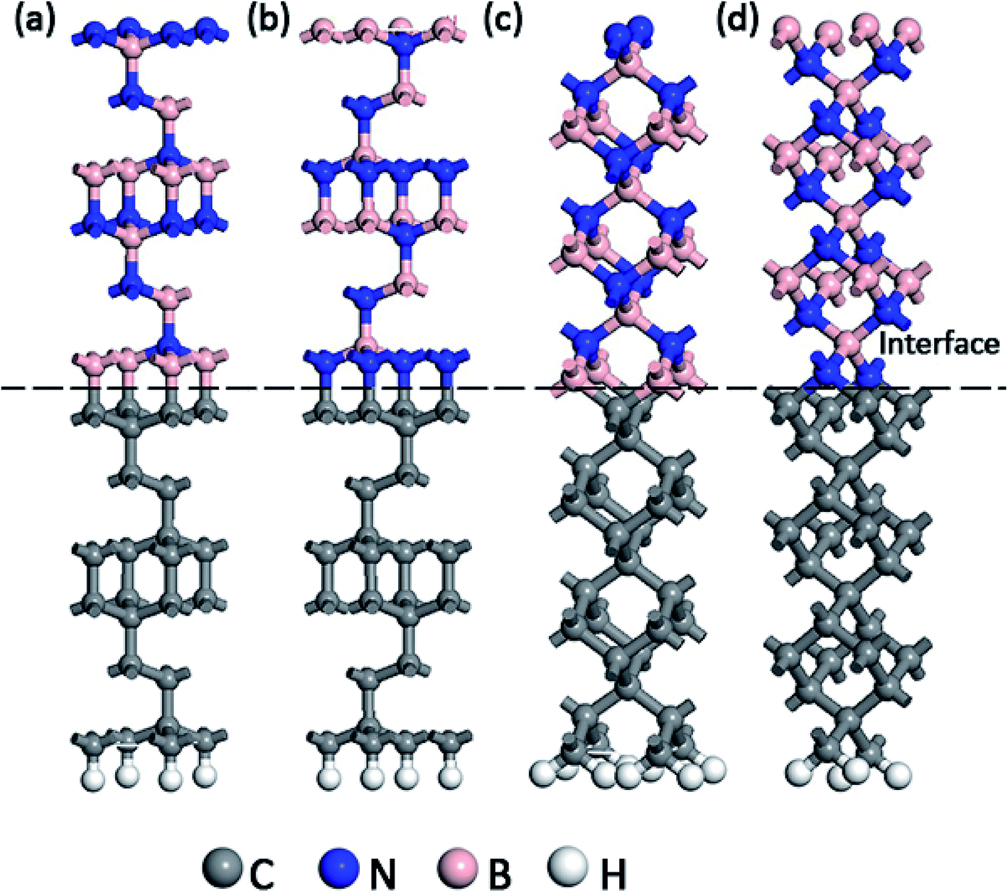
In the present work, the experimental lattice constant of c-BN and diamond were assumed to be 0.365 nm and 0.357 nm respectively.17,18 An initial diamond (111) slab model was composed of 12C atomic layers with 24 atoms in total. The initial c-BN (111) slab model was consisted of 2 cycles, 12 layers of B or N atom with 24 atoms altogether. The initial (100) surface models of c-BN and diamond were cut out using the same method, both of which were composed of 3 cycles, 12 atomic layers with 27 atoms in total. All the initial models of c-BN and diamond were thick enough to recover the bulk behavior far from the interface. Besides, all the initial slab models were optimized for the following calculations. Meanwhile, we confirmed the calculation parameters by convergence tests during the process of optimization. The hetero-structure was established directly without the cell expanding and coordinate transformation, owing to their low lattice mismatch of 4.6%. A-20 Å-thick vacuum layer was added to separate the surfaces in adjacent cells in the z-direction to eliminate the interactions between them. As shown in Fig. 1, four kinds of atomic bonding configurations of C–B (111) for c-BN/diamond hetero-interface, C–N (111) for c-BN/diamond hetero-interface, C–B (100) for c-BN/diamond hetero-interface and C–N (100) for c-BN/diamond hetero-interface were calculated. The Cartesian and fractional position of the bottom cycle of diamond were fixed in order to simulate the condition of substrate while other atoms moved freely. The surface atomic relaxations have little effect on the interface atomic structure. Hydrogen atoms are used to passivate the bottom surface C atoms of the diamond crystal.19
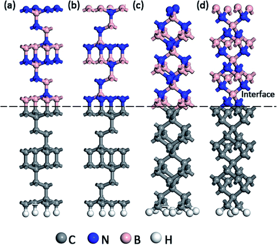 |
| | Fig. 1 Slab models of (111) c-BN/diamond hetero-interface with C–B (a) and C–N (b) bonding configuration and (100) c-BN/diamond hetero-interface with C–B (c) and C–N (d) bonding configuration, respectively. | |
The total-energy and physical properties were calculated based on the density functional theory (DFT) within the generalized gradient approximation (GGA) as implemented in the commercial CASTEP code.20–22 In order to avoid the difficulties on performance of the calculations with high accuracy, the pseudo-potentials adopted in the calculations were plane-wave ultrasoft pseudo-potential (USPP), suggested by Vanderbilt.23 Valence electron configurations for the elements were 2s2 2p2 for C, 2s2 2p1 for B, and 2s2 2p3 for N. For the energy minimization, the bottom cycle of C atoms and the layer of H atoms in diamond slabs were fixed to simulate a thick diamond substrate. In order to ensure a sufficient sampling density, convergence tests were performed to obtain reasonable values of k-points and cut-off energy.24 Thus, the plane wave basis set was included and truncated with a cut-off energy of 800 eV. The Monkhorst–Pack scheme was used for the Brillouin zone integration with an 8 × 8 × 1 k-point mesh, resulting in the electronic total energy well converged to 10−4 eV per cell. The relaxation of the atomic structure of the c-BN/diamond hetero-structure was carried out by calculating the Hellmann–Feynman forces until the force tolerance was 0.05 eV Å−1, the maximum displacement tolerance was 2 × 10⁻³ and the max. stress was 0.1 GPa.
3 Results and discussion
3.1. Optimized structure and stability
Prior to the total energy calculation, the bond length has been simulated as an increasing layer number of c-BN slabs to obtain a reasonable model. The calculated values of bond length are shown in Table 1. As the layer number is increased from 6 to 12, the initial bond length of C–B or C–N (1.517 Å) are gradually increased for (111) configurations, while it remains stale after the layer number exceeds 12. Contrarily, the bond length of C–B or C–N slightly fluctuates around the initial value of 1.663 Å for (100) configuration. Thus, the bond length of C–B or C–N at (111) c-BN/diamond hetero-interface converges with the increase of slab until 12 or 14, while the values for (100) hetero-interface are irregular. Particularly, it is worth mentioning that the c-BN exhibits theoretically a flat layered structure similar to the sp2-hexagonal phase when the layer of c-BN slab used in the calculations is less than 8 for C–B bonding in (100) c-BN/diamond model. This is clearly coincident with the experimental observations that the h-BN interfacial layer forms preferentially before the c-BN nucleates at the initial stage.25,26 Obviously, the resultant values of bond lengths of B–N are slightly larger than the experimental ones, which may due to the fact that GGA always expects a large electron density gradients in the system.22 For B–C (111) hetero-interface, the variety between 12 and 14 layers models were relatively small and the 12 layers model have a better periodicity for calculation and analysis. Nevertheless, the model composed of 12-layers of c-BN and 12-layers of diamond is reasonable enough to calculate their associated properties subsequently. To compare with the models of (111) hetero-interface, the layers of the c-BN on (100) hetero-interface were also used 12. Thus, the hetero-structures consisting of 48 atoms and 54 atoms have been used in the following calculations with the respect to the system of (111) and (100) c-BN/diamond, individually.
Table 1 The bond length (Å) of (111) and (100) c-BN/diamond hetero-interface with the increase of slab from 6 to 16
| Hetero-interface |
Interface-bonding |
6 |
8 |
10 |
12 |
14 |
16 |
| (111) |
C–B |
— |
— |
1.646 |
1.648 |
1.650 |
1.650 |
| (111) |
C–N |
1.517 |
1.522 |
1.523 |
1.524 |
1.524 |
1.524 |
| (100) |
C–B |
1.672 |
1.679 |
1.677 |
1.672 |
1.675 |
1.673 |
| (100) |
C–N |
1.633 |
1.635 |
1.642 |
1.638 |
1.640 |
1.639 |
To gain insights into optimized structure of the interface and offer a deeper understanding of their stability, we performed density functional theory calculations, taking into account both the C–B and C–N bonding configurations for (100) and (111) c-BN/diamond hetero-structures, as illustrated in Fig. 1 In order to investigate the thermodynamic stability of these four types of hetero-structures, the interface formation energy is calculated according to the following relationship:27
where
EBN/C,
EC and
EBN represent the total energies of c-BN/diamond hetero-structure, the corresponding part of the c-BN and diamond slab, respectively,
A represent the interface area.
28 The total energies of c-BN and diamond slabs are calculated with the same unit cell size, number of
k-points and cutoff energy as those of the hetero-interface. As listed in
Table 2, the calculated interface formation energies are 1.11, 0.70, 0.86, 0.58 eV corresponding to the C–B (111) c-BN/diamond, C–N (111) c-BN/diamond, C–B (100) c-BN/diamond and C–N (100) c-BN/diamond hetero-structures, respectively. Moreover, all the electronic properties have been calculated without the van der Waals (vdW) correction since vDW interaction does not alter the interface formation energy too much in the hetero-structures.
29 According to the definition, the interface formation energy should be positive. The more stable, the calculated formation energy values should be larger. Therefore, in the present calculations, the (111) c-BN/diamond hetero-structures are more energetically favorable than (100) hetero-structures. Furthermore, c-BN/diamond hetero-structures with C–B configuration are more energetically favorable than the hetero-structures with C–N configuration for both (111) and (100) interface in general. The calculations reveal that C–B bond might be the most possible energetically favored bonding configuration in c-BN/diamond epitaxy, consistent with the previous experimental observations.
30
Table 2 The binding energy of different hetero-interface
| Hetero-interface |
Interface-bonding |
EC (eV) |
EBN (eV) |
EBN/C (eV) |
E (eV) |
| (111) |
C–B |
−1869.34811 |
−2097.34592 |
−3973.88694 |
1.11133 |
| (111) |
C–N |
−1869.92156 |
−2097.65491 |
−3972.15663 |
0.70033 |
| (100) |
C–B |
−1264.90022 |
−2087.67366 |
−3358.30235 |
0.86070 |
| (100) |
C–N |
−1264.89892 |
−2087.67333 |
−3356.39852 |
0.58042 |
3.2. Band structure and density of states
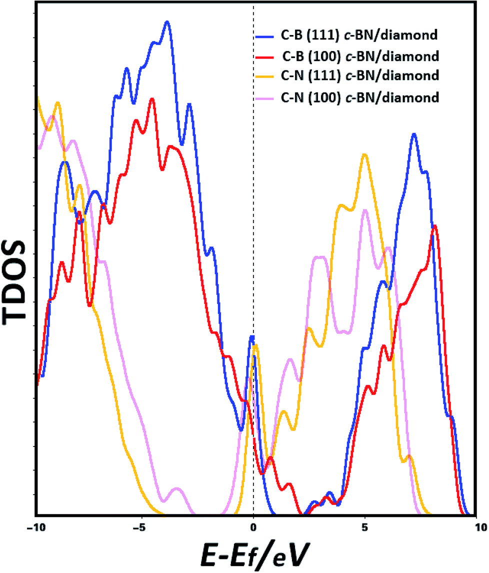
In order to predict the origin of the interface states, the electronic states at Fermi level (EF) have been calculated. The band structures are plotted along high symmetry k-points as shown in Fig. S1(a)–(d) in ESI.† We find the band structures of (100) hetero-interface have indirect band gaps. Thus, we discuss the PDOSs of (100) hetero-interface while the following analysis is mainly focused on the (111) hetero-structures. The calculated total densities of states (TDOSs) of the interfaces of C–B (111) c-BN/diamond, C–B (100) c-BN/diamond, C–N (111) c-BN/diamond and C–N (100) c-BN/diamond hetero-structures are shown in Fig. 2 Interestingly, the calculations of TDOSs predict that the electronic states at EF emerge at the interfaces of all the four cases, indicating that the interfaces show a full metallic character. Especially, dramatic increase of the TDOSs can be observed near the Fermi level for the (111) c-BN/diamond hetero-interfaces with both C–B and C–N configurations.
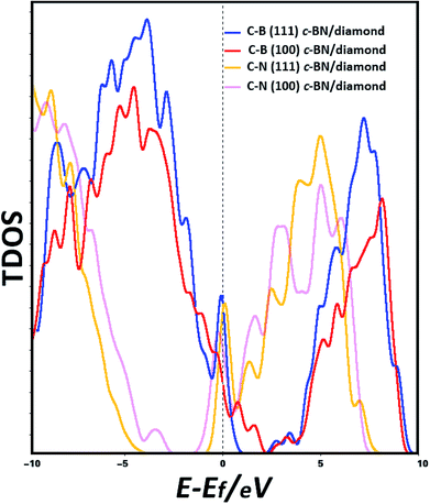 |
| | Fig. 2 Calculated TDOSs of (111) c-BN/diamond and (100) c-BN/diamond hetero-structures with C–B bonding configuration, (111) c-BN/diamond and (100) c-BN/diamond hetero-structures with C–N bonding configuration, with a vertical dashed line indicating Fermi level. | |
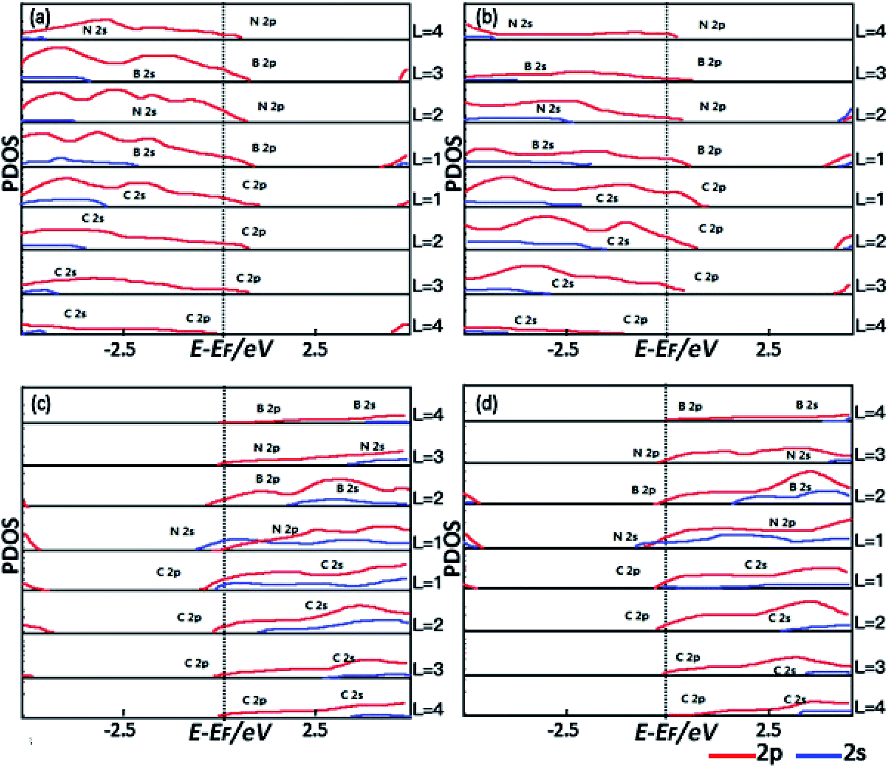
To further understand the spatial evolution of the electronic structure of the hetero-structures from the epitaxy interface to the bulk, the formation of interface states and the change of the density of the interface states for all the spins near EF are further studied by the layer-projected partial density of states (LPDOSs) as shown in Fig. 3(a)–(d) corresponding to the C–B (111) c-BN/diamond, C–B (100) c-BN/diamond, C–N (111) c-BN/diamond and C–N (100) c-BN/diamond hetero-interface, respectively. The PDOSs are calculated by averaging the total DOSs per layer for each atom in the layer. To clearly identify the electronic states, the PDOSs of the hetero-structures are calculated by starting from the interface region extending to the bulk c-BN and diamond regions. The L denotes the number of the atomic layers and increases with increasing separation from the interface. Fig. 3(a) shows the PDOSs of the (111) c-BN/diamond hetero-structure with C–B bonding configuration in which the interface states mainly result from B 2p at the first layer and third layer and N 2p at the second layer and fourth layer of the c-BN slab near the interface. Such tendency in the PDOSs varying with increasing atomic layer (L) is similar to those for the (100) c-BN/diamond with C–B configuration as well (Fig. 3(b)). Besides, according to the diamond's LPDOSs, it is revealed that the most contribution to the density of the interface states near EF is from C 2p orbital within three C atomic layers at the interface of both (111) and (100) c-BN/diamond hetero-structures. In comparison, the LPDOSs results of c-BN/diamond hetero-structure (111) (Fig. 3(c)) and (100) (Fig. 3(d)) with C–N bonding configuration indicate that the main contribution to the density of the interface states near the EF is from the first layer of N 2s, N 2p and the second layer of B 2p orbital of c-BN slabs and the first layer of C 2s 2p and the second layer of C 2p orbital of diamond slabs. Thus, unlike the C–B bonding configuration of which the density of interface states are all from p-orbital, for the C–N bonding configuration of c-BN/diamond hetero-interface, a large number of electronic states from s-orbital appear lying near the Fermi level due to the strong interaction through the interfacial C and N.
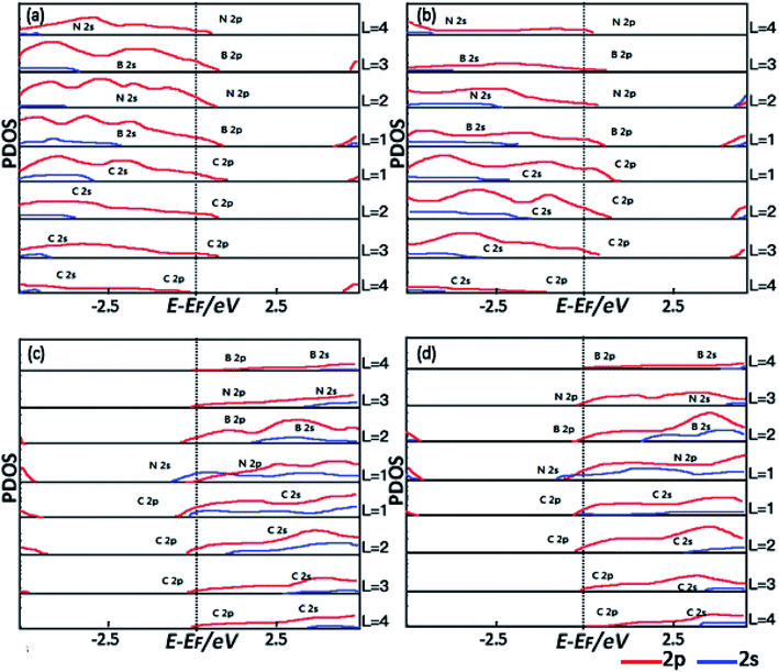 |
| | Fig. 3 The PDOSs for (111) c-BN/diamond (a) and (100) c-BN/diamond (b) hetero-structures with C–B bonding configuration, (111) c-BN/diamond (c) and (100) c-BN/diamond (d) with C–N bonding configuration. Layer number is counted from the interface to the surface. The dashed vertical line indicates the Fermi energy. | |
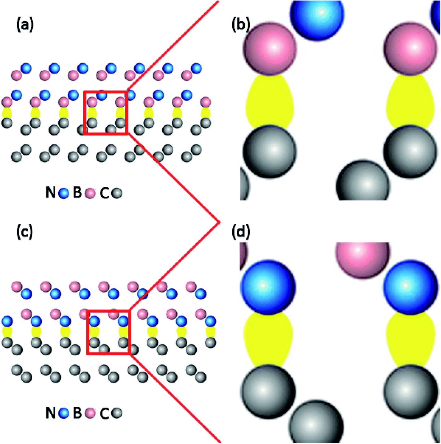
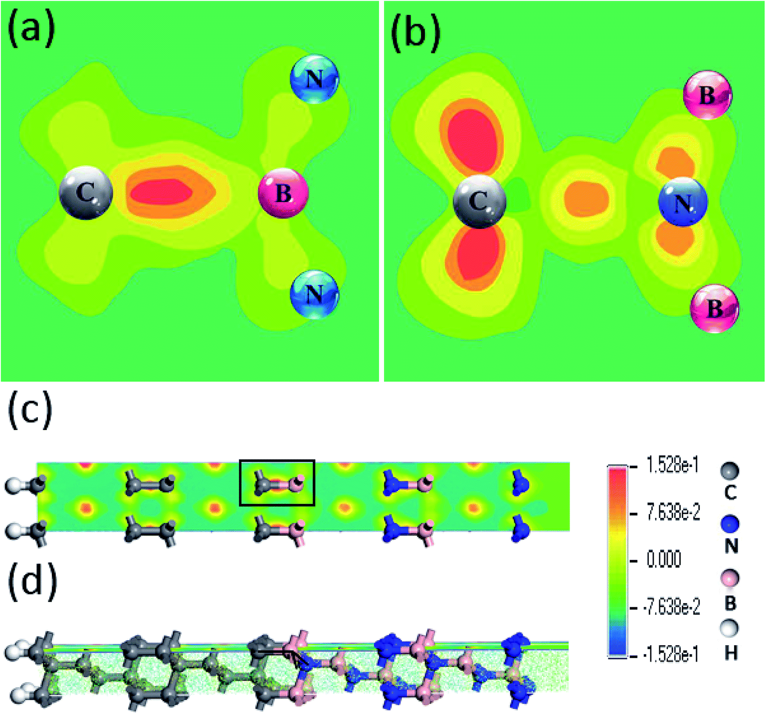
Furthermore, in order to dig the impacts of C–B and C–N configurations on the electronic states, the spatial charge distributions in electronic wavefunction paralleled to bonding directions in the (111) and (100) c-BN/diamond hetero-structures have been compared directly as shown in Fig. 4(a) and (b). One can clearly notice that the electron charges have been confined more approaching to the C atoms in the C–B bonds other than to the N atoms in the C–N bonds. Nevertheless, the electronic states for all the current four models of c-BN/diamond hetero-interface near Fermi level mainly come from the interfacial C sp orbital and are confined to the interface, which has been observed in a (111) diamond/c-BN system previously.30
 |
| | Fig. 4 Charges distribution near the Fermi level of (111) hetero-interface with C–B (a) and C–N (c) bonding configurations, in which (b) and (d) show the partial enlarged details of (a) and (c). | |
3.3. Charge transfer
To clarify the bonding mechanism and the transfer of electrons between the adjacent layers at the interface of the (111) c-BN/diamond hetero-structure, electron density difference along the direction perpendicular to the interface is calculated. Fig. 5(a) and (b) shows the contour plots of charge density differences for the interfaces of c-BN/diamond with C–B and C–N, respectively. The plane was selected as it sliced through the C–B bond and C–N bond which makes it clear to observe the bonding strength on this interface. Fig. 5(c) and (d) shows the top view and side view for the interface layer of C–B bond. The parts marked by real line were enlarged as is shown in Fig. 5(a) and (b). The charge distribution on each atom is severely distorted to their adjacent atoms, implying the strong covalent characteristics in both bonding configurations.30 It is obvious that the C–B bonds (Fig. 5(a)) are stronger than the C–C bonds, while the C–N bonds (Fig. 5(b)) are far weaker than the C–C bonds. The majority of charges of C–B bond in the interface are localized on C and B, other than that in the adjacent C–C bond and B–N bond. Furthermore it is clearly seen that charge is depleted in the region of B plane, meanwhile, the charge is accumulated in the region of C plane near the interface. Comparing both bonding configurations, it strongly shows that the C–B bond exhibits more strong covalent character than the C–N bond, which agrees with the above results of interface formation energy calculations. According to Fig. 3(c) and (d), the hybridization takes place between C 2p, N 2s 2p and B 2p from the PDOS for the (111) c-BN/diamond hetero-structure with C–N interface configuration, meanwhile, that with C–B interface configuration hybridizes by C 2p, B 2p and N 2p orbital. The sp2-like bond hybridized by 3 orbital are vulnerable to rupture than the sp3-like bond hybridized by 4 orbital, thus, the introduction of s-orbital may weaken the charge transfer near the hetero-interface and hindering the formation of bonding.31 Therefore, in context of the results of total energy calculation and charge density difference, the C–B bonds are most stable constructions, which may possibly occur in the heteroepitaxially growth of c-BN on diamond. On the other hand, it has been reported that the deposition of N should be following B as it is difficult to form a monolayer of N on diamond surface because of the desorption of N addimers.32
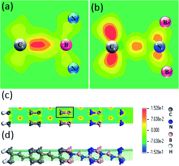 |
| | Fig. 5 Charge density difference for interfaces of (111) c-BN/diamond hetero-structure with C–B (a) and C–N (b) bonding configurations, respectively. The parts marked by real line in top view (c) and side view (d) for the C–B bond interface layer were enlarged for a clear observation. | |
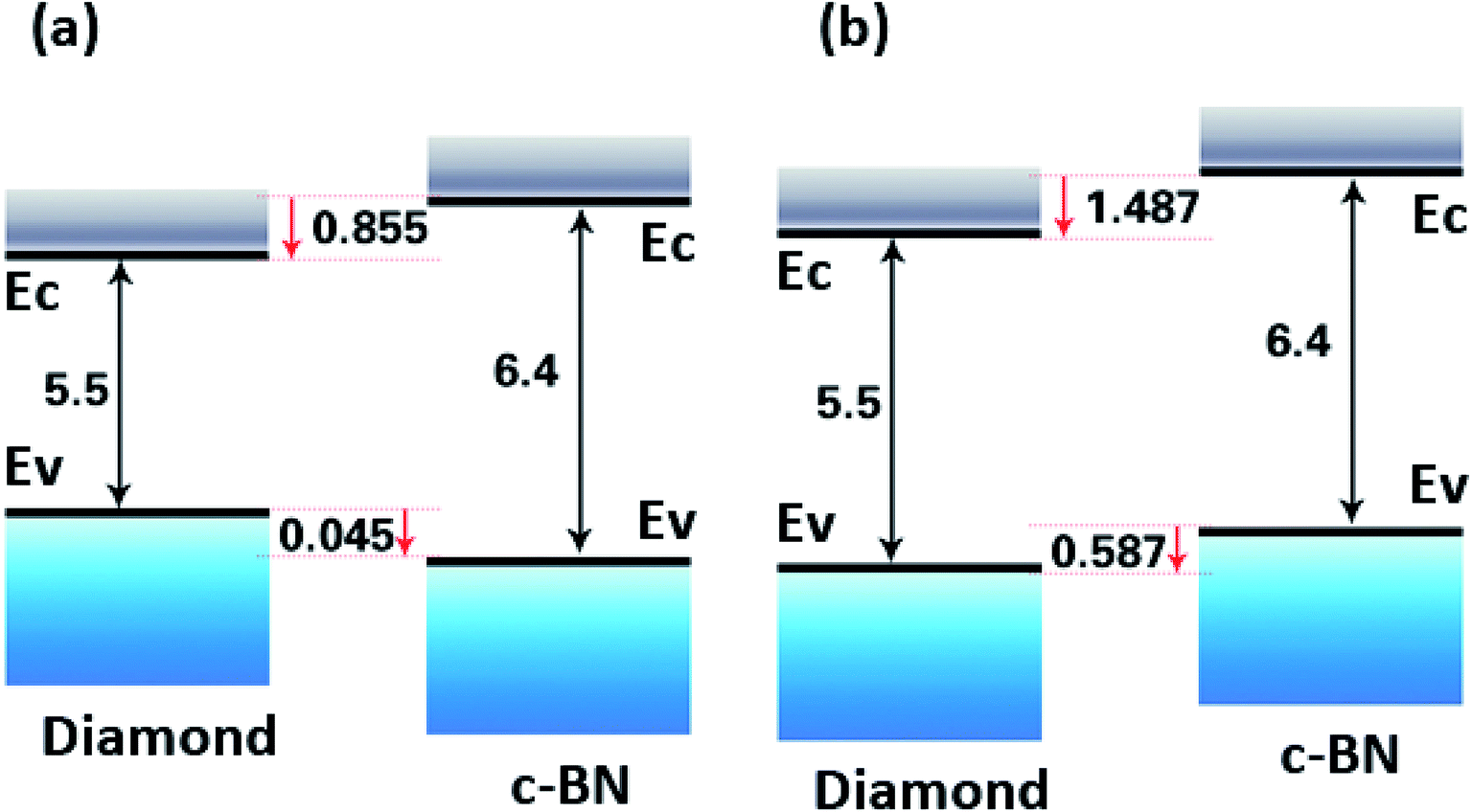
3.4. Band offsets
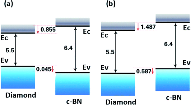
The energy band offsets or band discontinuities at the (111) hetero-interface of both C–B and C–N bonding configurations were carried out. The band offsets can be determined directly from the partial density of states (PDOSs) calculations, in which the valence band offset at the interface is the energy difference between the tops of the valence bands of the c-BN layer and the diamond layer.32–34 Although this method can determine the band offset directly, the results are usually sensitive to the computational condition such as the number of k-points, cut-off energy, size of a supercell, etc. It is known that the band gap is usually underestimated by the DFT method, resulting in the lowered lying conduction band (see Table S1(a)–(d) in ESI†). Therefore, we focus on the alignment of the valence-band edge (EV) and Fermi level (EF). The band gap values of 6.4 eV and 5.5 eV of c-BN and diamond are used to determine the conduction-band edge, respectively.14
The band offsets of both C–B bond and C–N bond at the (111) hetero-interfaces have been both calculated and the results are summarized in Table 3. As is shown, for the C–B bond structure, the VBM of c-BN is positioned at 0.56989 eV, while the VBM of diamond is positioned at 0.61523 eV, resulting in a VBO of about 0.045 eV. For the C–N bond structure, the VBM of c-BN is positioned at −2.35441 eV, while the VBM of diamond is positioned at −2.94104 eV, giving a VBO of about 0.587 eV.
Table 3 The calculated values of the valance band for C–B and C–N at (111) c-BN/diamond hetero-interface
| Interface-bonding |
c-BN (eV) |
Diamond (eV) |
VBO (eV) |
| C–B |
0.56989 |
0.61523 |
−0.04534 |
| C–N |
−2.35441 |
−2.94104 |
0.58663 |
Based on the calculation results, the band offsets are schematically illustrated in Fig. 6(a) and (b) The VBM of c-BN is positioned at 0.045 eV below that of diamond for C–B bonding configuration, with the CBM of c-BN at 0.855 eV above that of diamond for the C–B interface configuration (Fig. 6(a)). The VBM of c-BN is positioned at 0.587 eV above that of diamond, with the CBM of c-BN at 1.487 eV above that of diamond for the C–N interface configuration (Fig. 6(b)). The latter is accordance to a recent report in which VBM of c-BN was inferred to be 0.8 eV above that of diamond for C–N interfacial bonding.36 However, the previous theoretical calculations demonstrated that the c-BN VBM positioned at least 1.9 eV below the diamond VBM in the (100) surface for C–B bondings and 0.13 eV for C–N bondings.35 In addition, the c-BN VBM was found to be 0.71 eV lower than that of diamond as to the (110) hetero-interface with one mixed C–B and C–N layer.15 The differences in these calculated and experimental band offset values strongly suggest that the interface bonding configuration should be considered.
 |
| | Fig. 6 Schematic representation of the relative position of the valence band and conduction band edges of (111) c-BN/diamond hetero-structure with C–B (a) and C–N (b) bonding configurations. | |
4 Conclusions
In this work, we establish and optimize four kinds of hetero-structures on (100) and (111) surface with different atomic bonding configurations by the first-principle calculations. 12-layers of c-BN and 12 layers of diamond hetero-structures are found reasonable enough for the calculations of properties according to the convergence of band length and band gap. The hetero-interface with C–B configuration is the most energetically favorable structure under (111) and (100) surface of diamond. The results of LPDOSs reveal that the contribution to the densities of the interface states neat EF is mainly from C 2p, B 2p and N 2p for C–B bonding configuration and C 2p, B 2p, and N 2s 2p for C– N bonding configuration in both (100) and (111) hetero-interface. The band offsets are also calculated, resulting in a VBO of about 0.045 eV for C–N bond and about 0.587 eV for C–B bond on (111) hetero-interface.
Conflicts of interest
There are no conflicts to declare.
Acknowledgements
The financial supports by the National Natural Science Foundation of China (Grants No. 51572105, 51872113 and 61504046) are specially acknowledged. H. Yin is grateful to the Scientific Research Foundation for the Returned Overseas Chinese Scholars, State Education Ministry. The financial supports from the Scientific Research Foundation for the Returned Overseas of Jilin Province are also appreciated.
Notes and references
- M. Sajjad, G. Morell and P. Feng, ACS Appl. Mater. Interfaces, 2013, 5, 5051–5056 CrossRef CAS.
- L. Vel, G. Demazeau and J. Etourneau, Mater. Sci. Eng., B, 1991, 10, 149–164 CrossRef.
- V. N. Mochalin, O. Shenderova, D. Ho and Y. Gogotsi, Nat. Nanotechnol., 2012, 7, 11–23 CrossRef CAS.
- I. Aharonovich, S. Castelletto, D. A. Simpson, C. H. Su, A. D. Greentree and S. Prawer, Rep. Prog. Phys., 2011, 74, 076501 CrossRef.
- Y. Tian, X. Bo, D. Yu, Y. Ma, Y. Wang, Y. Jiang, W. Hu, C. Tang, Y. Gao and K. Luo, Nature, 2013, 493, 385–388 CrossRef CAS.
- V. L. Solozhenko, O. O. Kurakevych and G. Y. Le, Adv. Mater., 2012, 24, 1540–1544 CrossRef CAS.
- Q. Huang, D. Yu, B. Xu, W. Hu, Y. Ma, Y. Wang, Z. Zhao, B. Wen, J. He and Z. Liu, Sci. Found. China, 2014, 510, 250–253 CAS.
- M. Füner, C. Wild and P. Koidl, Appl. Phys. Lett., 1998, 72, 1149 CrossRef.
- X. W. Zhang, H.-G. Boyen, N. Deyneka, P. Ziemann, F. Banhart and M. Schreck, Nat. Mater., 2003, 2, 312 CrossRef CAS.
- W. J. Zhang, I. Bello, Y. Lifshitz, K. M. Chan, Y. Wu, C. Y. Chan, X. M. Meng and S. T. Lee, Appl. Phys. Lett., 2004, 85, 1344–1346 CrossRef CAS.
- S. Ohmagari, K. Srimongkon, H. Yamada, H. Umezawa, N. Tsubouchi, A. Chayahara, S. Shikata and Y. Mokuno, Diamond Relat. Mater., 2015, 58, 110–114 CrossRef CAS.
- J. Yamauchi, M. Tsukada, S. Watanabe and O. Sugino, Phys. Rev. B: Condens. Matter Mater. Phys., 1996, 54, 5586 CrossRef CAS.
- W. E. Pickett, Phys. Rev. B: Condens. Matter Mater. Phys., 1988, 38, 1316 CrossRef CAS.
- G. M. He, Y. M. Zheng, R. Z. Wang and S. P. Li, Solid State Commun., 2001, 118, 287–290 CrossRef CAS.
- K. Yamamoto, K. Kobayashi, T. Ando, M. Nishitani-Gamo, R. Souda and I. Sakaguchi, Diamond Relat. Mater., 1998, 7, 1021–1024 CrossRef.
- S. B. Li, T. Zhu, L. C. Dong and M. D. Dong, New J. Chem., 2018, 42, 17644 RSC.
- L. A. Bursill, J. L. Hutchison, N. Sumida and A. R. Lang, Nature, 1981, 292, 518–520 CrossRef CAS.
- Y. Zhang, H. Sun and C. Chen, Phys. Rev. B: Condens. Matter Mater. Phys., 2006, 73, 2368–2381 Search PubMed.
- H. Heidari, S. Afshari and E. Habibi, RSC Adv., 2015, 5, 94201–94209 RSC.
- K. M. O'Donnell, T. L. Martin, N. A. Fox and D. Cherns, Phys. Rev. B: Condens. Matter Mater. Phys., 2010, 82, 3893–3898 Search PubMed.
- V. Milman, B. Winkler, J. A. White, C. J. Pickard, M. C. Payne, E. V. Akhmatskaya and R. H. Nobes, Int. J. Quantum Chem., 2015, 77, 895–910 CrossRef.
- C. Stampfl and C. G. V. D. Walle, Phys. Rev. B: Condens. Matter Mater. Phys., 1999, 59, 5521–5535 CrossRef CAS.
- D. Vanderbilt, Phys. Rev. B: Condens. Matter Mater. Phys., 1990, 41, 7892 CrossRef.
- L. Yuan, L. I. Zhenyu, J. Yang and J. G. Hou, Phys. Chem. Chem. Phys., 2012, 14, 8179–8184 RSC.
- B. Mårlid, K. Larsson and J.-O. Carlsson, Phys. Rev. B: Condens. Matter Mater. Phys., 2001, 64, 184107 CrossRef.
- X. W. Zhang, Y. J. Zou and B. Wang, J. Mater. Sci., 2001, 36, 1957–1961 CrossRef CAS.
- N. R. D'Amico, G. Cantele, C. A. Perroni and D. Ninno, J. Phys.: Condens. Matter, 2015, 27, 015006 CrossRef.
- W. R. Lambrecht and B. Segall, Phys. Rev. B: Condens. Matter Mater. Phys., 1989, 40, 9909–9919 CrossRef CAS.
- K. P. Wu, W. F. Ma, C. X. Sun, C. Z. Chen, L. Y. Ling and Z. G. Wang, Chin. Phys. B, 2018, 27, 522–529 Search PubMed.
- C. Chen, Z. Wang, T. Kato, N. Shibata, T. Taniguchi and Y. Ikuhara, Nat. Commun., 2015, 6, 6327 CrossRef CAS.
- H. Bu, H. Zheng, H. Zhou, H. Zhang, Z. Yang, Z. Liu, H. Wang and Q. Xu, RSC Adv., 2019, 9, 2657–2665 RSC.
- H. Koga, T. Miyazaki, S. Watanabe and T. Ohno, J. Appl. Phys., 2004, 43, 7944–7946 CrossRef CAS.
- J. Robertson and L. Lin, Appl. Phys. Lett., 2011, 99, 294 CrossRef.
- K. Hirose, K. Sakano, H. Nohira and T. Hattori, Phys. Rev. B: Condens. Matter Mater. Phys., 2001, 64, 155325 CrossRef.
- O. Sharia, A. A. Demkov, G. Bersuker and B. H. Li, Phys. Rev. B: Condens. Matter Mater. Phys., 2007, 75, 35306 CrossRef.
- J. Shammas, Y. Yang, X. Wang, F. A. Koeck, M. R. McCartney, D. J. Smith and R. J. Nemanich, Appl. Phys. Lett., 2017, 111, 171604 CrossRef.
Footnote |
| † Electronic supplementary information (ESI) available. See DOI: 10.1039/c9ra00784a |
|
| This journal is © The Royal Society of Chemistry 2019 |
Click here to see how this site uses Cookies. View our privacy policy here. 
 Open Access Article
 This Open Access Article is licensed under a Creative Commons Attribution-Non Commercial 3.0 Unported Licence
 ,
Yujing Li,
Yuyuan Zhang
,
Yujing Li,
Yuyuan Zhang