
 Open Access Article
 This Open Access Article is licensed under a
 Creative Commons Attribution 3.0 Unported Licence
Controlled inter-state switching between quantized conductance states in resistive devices for multilevel memory†
Sweety Deswal ab,
Rupali R. Malodec,
Ashok Kumarab and
Ajeet Kumar*ab
ab,
Rupali R. Malodec,
Ashok Kumarab and
Ajeet Kumar*ab
aAcademy of Scientific and Innovative Research, CSIR-National Physical Laboratory Campus, Dr. K. S. Krishnan Marg, New Delhi 110012, India. E-mail: kumarajeet@nplindia.org
bCSIR-National Physical Laboratory, Dr. K. S. Krishnan Marg, New Delhi 110012, India
cMaulana Azad National Institute of Technology, Bhopal, Madhya Pradesh 462003, India
First published on 25th March 2019
Abstract
A detailed understanding of quantization conductance (QC), the correlation with resistive switching phenomena and controlled manipulation of quantized states is crucial for realizing atomic-scale multilevel memory elements. Here, we demonstrate highly stable and reproducible quantized conductance states (QC-states) in Al/niobium oxide/Pt resistive switching devices. Three levels of control over the QC-states, required for multilevel quantized state memories, like, switching ON to different quantized states, switching OFF from quantized states, and controlled inter-state switching among one QC state to another has been demonstrated by imposing limiting conditions of stop-voltage and current compliance. The well-defined multiple QC states along with a working principle for switching among various states show promise for implementation of multilevel memory devices.
Driven by the demand for improved computing capability, the semiconductor industry is following the extension of Moore's law which says that the density of transistors in an integrated circuit doubles every two years. However the current technology, charge based flash memory, has reached its limit of miniaturization.1,2 Also, all existing devices are limited to two stable memory states (i.e., “0” and “1”). Increasing the number of stable states, from bi-stability to multi-stability, will be an effective method for producing high-density and efficient memory devices.
As one for the most promising candidates for future non-volatile memories, resistive random access memory (ReRAM) with simple two-terminal sandwiched structured devices exhibit attractive performances due to their scalability down to the atomic level, CMOS compatibility, low-power consumption, and high-speed features.3,4 It has been proposed that the multiple stable states available in the resistive switches can be used for multilevel storage for ultrahigh density memories.5 Existence of stable multistates has been demonstrated in resistive switching,6–14 ferroelectric15–20 and phase change21–25 memory devices. Atomic point contact based QC observed in resistive switching devices has also been demonstrated for memory applications.26–31 However, controlled manipulation of multiple stable states for potential application in multilevel memory is yet to be achieved.
Several kinds of control over stable QC-states in a resistive switching device are required to achieve multilevel quantized state memories. These particular kinds of devices have not been fully explored, partly because of the lack of appropriate materials and lack of design & working principles. Many groups have demonstrated quantization in several ReRAM32–36 as well as in atomic switch29,37–39 devices. The conditions to achieve different quantized states either with current compliance40,41 or with stop voltage37,40 have been reported. Also, there is some understanding about the stability of these states with respect to time.35,37,42,43 However, conditions for controlled inter-QC-state switching, essential for multilevel memory, have not been reported.
Here, we demonstrate control over the events of switching ON to different QC-states, switching OFF from QC-states, and inter-QC-state switching in Al/niobium oxide/Pt device. Firstly, stable and reproducible QC-states with integer and half-integer multiples of quantum of conductance (G0 = 2e2/h ∼77.4 μS) were achieved, indicating formation of well-controlled atomic point contacts in the conducting filaments. Then, the devices were manipulated to exhibit hundreds of different inter-QC-state switching, both in the direction of SET (higher G0) or RESET (lower G0) starting from any particular QC-state. The initial and final QC-states, for each switching event, were found to be stable. The device exhibited longer retention times for higher QC-states. Rules for controlled switching are evolved with stop-voltage and current compliance limits during current–voltage (I–V) measurements. The working principles demonstrated in this work, to achieve QC-states and to induce inter-QC-state switching, is a crucial step towards realization of multilevel memory devices.
Switching ON to QC-state: The resistive switching and QC characteristics are demonstrated using I–V measurements on Al/Nb2O5/Pt devices in air at room temperature. These devices, in their pristine state, were found in high resistance OFF state (HRS) of the order of ∼109 Ω. Initially, the device was switched to low resistance ON state (LRS) at a forming voltage ∼4 V with current compliance (Ic) of 5 μA, as shown in the inset of Fig. 1a. After forming, with voltage sweeps, the device showed reproducible switching between LRS to HRS (RESET; voltage ∼ −0.4 to −1.2 V) and vice versa (SET; voltage ∼1.6–2.5 V), shown as semi-logarithmic I–V plots in Fig. 1a. These devices show both unipolar as well as bipolar switching characteristics in either polarities of the voltage (ESI Fig. S1†). In our previous work,34 unipolar switching behaviour of the Al/Nb2O5/Pt devices were presented and it was demonstrated that the conducting filament, after making the atomic point contact, grows in thickness atom-by-atom during SET voltage sweep. Here, in this work, conducting filaments were stabilized to achieve various QC-states. During the SET process, the LRS was controlled by applying voltage sweeps with different current compliance values of 100, 200, 300, 400 and 500 μA (Fig. 1b) and different resistance states of 9 kΩ, 6 kΩ, 4 kΩ, 2.9 kΩ and 2.3 kΩ, respectively, were achieved. These resistance states were stable and correspond to quantized conductance states of ∼1.5 G0, ∼2 G0, ∼3.5 G0, ∼4.5 G0, and ∼5.5 G0, respectively (Fig. 1c).
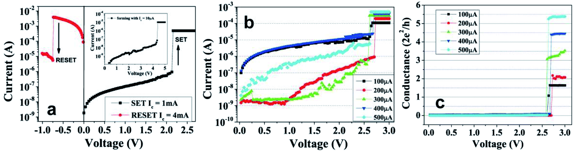 | ||
| Fig. 1 (a) Semi-logarithmic I–V characteristics of Al/Nb2O5/Pt device showing bipolar switching with SET and RESET in range of 1.6–2.5 V and –(0.4–1.2 V), respectively. The inset shows the electroformation step of the device. (b) The semi-logarithmic I–V plots of SET with various current compliances (Ic) values of 100, 200, 300, 400, 500 μA reaching to different LRS levels corresponding to quantized conductance states of ∼1.5 G0, ∼2 G0, ∼3.5 G0, ∼4.5 G0, and ∼5.5 G0, respectively. (c) The SET traces of (b) are plotted as conductance vs. voltage (G–V) to show distinguishable quantized LRS states obtained. | ||
QC-states achieved during SET sweeps with different Ic values were analyzed to determine the state distribution of the device conductance. Fig. 2a–f show that distinct and stable QC-states could be reproducibly achieved by varying Ic values. Histograms of conductance in the units of G0 for ∼300 switching cycles performed on an Nb2O5 device are shown for five different compliance currents upto 500 μA. After each SET event, the conductance state was estimated by applying a read voltage of 100 mV. The data was sorted in the bin size of 0.1 G0 and respective numbers were counted to plot the conductance histogram, shown in Fig. 2. QC-state of ∼1 G0 was achieved with 100 μA, where only a single conduction channel allows electron transport through the filament of the resistive switch. With the increase of current compliance, the conductance peak shifted towards higher conductance value. The QC-states of 2 G0, 3.5 G0, 4.5 G0, and 5.5 G0 were achieved with Ic of 200 μA, 300 μA, 400 μA, and 500 μA, respectively, as seen in Fig. 2b–e. As higher conductance states are gradually reached, it has been understood that the atomic rearrangements in the point contact allows more number of conduction channels to become available for electron transfer.31,34 The histogram with all five sets of each Ic, acquired from ∼300 curves of SET cycles is shown in Fig. 2f. It can be clearly seen that the devices exhibited quantized conductance peaks around integer and half-integer multiples of G0. Out of several switching cycles, 25 cycles with each Ic values 100, 200, 300, 400, 500 μA representing the median of the distribution of quantized state as plotted in Fig. 2a–e is shown in Fig. 2g. The well separated memory levels available in our devices meet one of the essential requirements for realizing multilevel ultra high density storage.
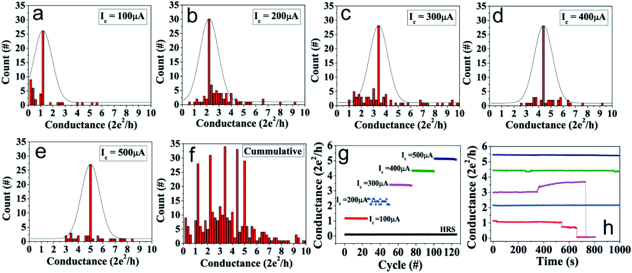 | ||
| Fig. 2 The histogram of quantized conductance values obtained during SET with Ic of (a) 100 μA (b) 200 μA, (c) 300 μA, (d) 400 μA, (e) 500 μA. Each plot shows the data of more than 60 cycles of SET for a particular Ic. (f) The cumulative data of all G0 (in Fig. 2a–e) obtained for ∼300 cycles of SET. (g) The median of the distribution shows distinct conductance states after SET with current compliance of 100, 200, 300, 400, 500 μA along with HRS is exhibited for 125 switching cycles. (h) The stability of corresponding quantized conductance states shown in (g). | ||
Stability of QC-states & retention time: To understand the stability of the quantized conductance states, retention time characteristics of different conductance states were studied. Different QC-states were achieved in different SET sweeps and their retention time was measured at 100 mV read voltage. Fig. 2h shows the retention time of >500 s for QC-states corresponding to 1 G0, 2 G0, 3.5 G0, 4.5 G0, and 5.5 G0. The retention time of different QC-states were observed to be increasing with increase in G0. In general, QC-states below 3 G0 were stable for less than 800 s, while the QC-states higher than 3 G0 were stable for more than 1000 s. However, on some occasions, stability over 1000 s were also observed for states <3 G0. Retention data of various other QC-states are shown in ESI Fig. S2a.† The stability of a particular QC-state depends on the strength of the corresponding conducting filament. The conducting filament diameter increases as the G0 of QC-states increase, thus making them more and more robust. The magnitude of applied read voltage during retention measurement was also found to influence the stability of QC-states (ESI Fig. S2b†).
Inter-QC-state switching: Once a device is switched ON to a particular QC-state, voltage sweep and current compliance conditions could be controlled to exhibit many different inter-QC-state switching in the device, be in the direction of SET (higher G0) or RESET (lower G0). Fig. 3 shows one set of four successive switching steps of inter-QC-state in SET direction of a particular device along with the corresponding QC-state retention time up to 100 s. The device was, firstly, SET to ∼2.5 G0 with Ic = 200 μA (Fig. 3a). In the subsequent voltage sweep with Ic = 300 μA, we induced an inter-QC-state switching from 2.5 G0 to ∼3 G0 state (Fig. 3b). Here, during the second sweep, the starting QC-state was found to be at 0.5 G0 instead of 2.5 G0. This change in state can be understood as instability of states below 3 G0, as discussed above. Further, the QC-state was successively switched from 3 G0 to 3.5 G0 (Fig. 3c), 3.5 G0 to 4 G0 (Fig. 3d) and 4 G0 to 4.5 G0 (Fig. 3e) during voltage sweeps with Ic = 400, 500 and 600 μA, respectively. All QC-states of the device were found to be stable for at least up to 100 s (Fig. 3h–j). The QC-states achieved during the inter-QC-state switching with Ic of 200–500 μA either matched with the peak values from the histogram of Fig. 2b–e, or fall within full-width half maxima of the peak distribution. The corresponding I–V traces of the conductance–voltage (G–V) traces shown in Fig. 3a–e are shown in the ESI Fig. S3.†
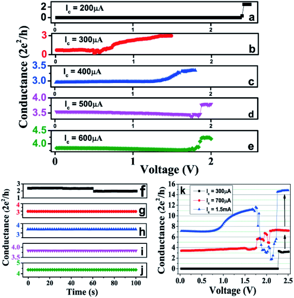 | ||
| Fig. 3 The interstate transitions between two quantized states with successive voltage sweeps during SET is exhibited in figures (a)–(e) with their corresponding final state stabilities in (f)–(j). (a) The device was first SET with Ic = 200 μA, reached to 2.5 G0. (b) In next voltage sweep with Ic = 300 μA, a state of ∼3 G0 is achieved. (c) In subsequent voltage sweep with Ic = 400 μA, state of ∼3 G0 switched to ∼3.5 G0. (d) Further increasing Ic to 500 μA, switching from ∼3.5 G0 to ∼4 G0 is induced. (e) And subsequently, in voltage sweep with Ic = 600 μA, state of 4 G0 switched to 4.5 G0. (f)–(j) Shows the stability of QC-states reached during switching steps (a)–(e). (k) The inter-QC-state switching between two quantized states with successive voltage sweeps with Ic = 300 μA, 700 μA and 1.5 mA is exhibited. | ||
The inter-QC-state switching where the Ic values were increased in steps of 400 μA and 800 μA were also performed. In Fig. 3k, the device was switched to ∼3 G0 state with Ic = 300 μA (black trace) and then in subsequent voltage sweep with Ic = 700 μA, the device switched to ∼7 G0 state (red trace). Further, as another voltage sweep was performed with Ic = 1.5 mA, the device switched from 7 G0 to 15 G0. While switching from 3 G0 to 7 G0, the device showed indications to stop at different intermediate QC-states, however, due to higher Ic limit, the devices stopped only at 7 G0. It appears that an Ic of more than 300 μA and less than 700 μA would have possibly stabilized the device at some intermediate QC-state. During the voltage sweep with Ic = 1.5 mA, the device exhibited instability around 12 G0 state (Fig. 3k, blue trace). Since, the device can switch in both unipolar and bipolar modes, it can be understood as the device's tendency to RESET in unipolar mode due to very high currents, however, the voltage was in the range of SET (1.5–2.5 V), thus the device switched to 15 G0.
The inter-QC-state switching was also controlled and reproducibly performed in RESET direction. Fig. 4 shows three successive steps of inter-QC-state switching of a device, where different stop voltages are used to control switching to different QC levels. The device was, firstly, SET to ∼20 G0 state. Then, an inter-QC-state switching from 20 G0 to 6 G0 was induced by a voltage sweep, where −1.0 V was kept as the stop-voltage (Vs), shown in Fig. 4a. In the subsequent sweeps, the QC-state switched from 6 G0 to 4.5 G0 (Fig. 4b) and from 4.5 G0 to 3.5 G0 (Fig. 4c), with Vs = −1.1 V and −1.2 V, respectively. In another subsequent sweep, the QC-state switched from 3.5 G0 to a very high resistance state (i.e. complete RESET) with Vs = −1.5 V, as shown in Fig. 4d. Each QC-state, after every switching, was found to be stable with time (Fig. 4e–h).
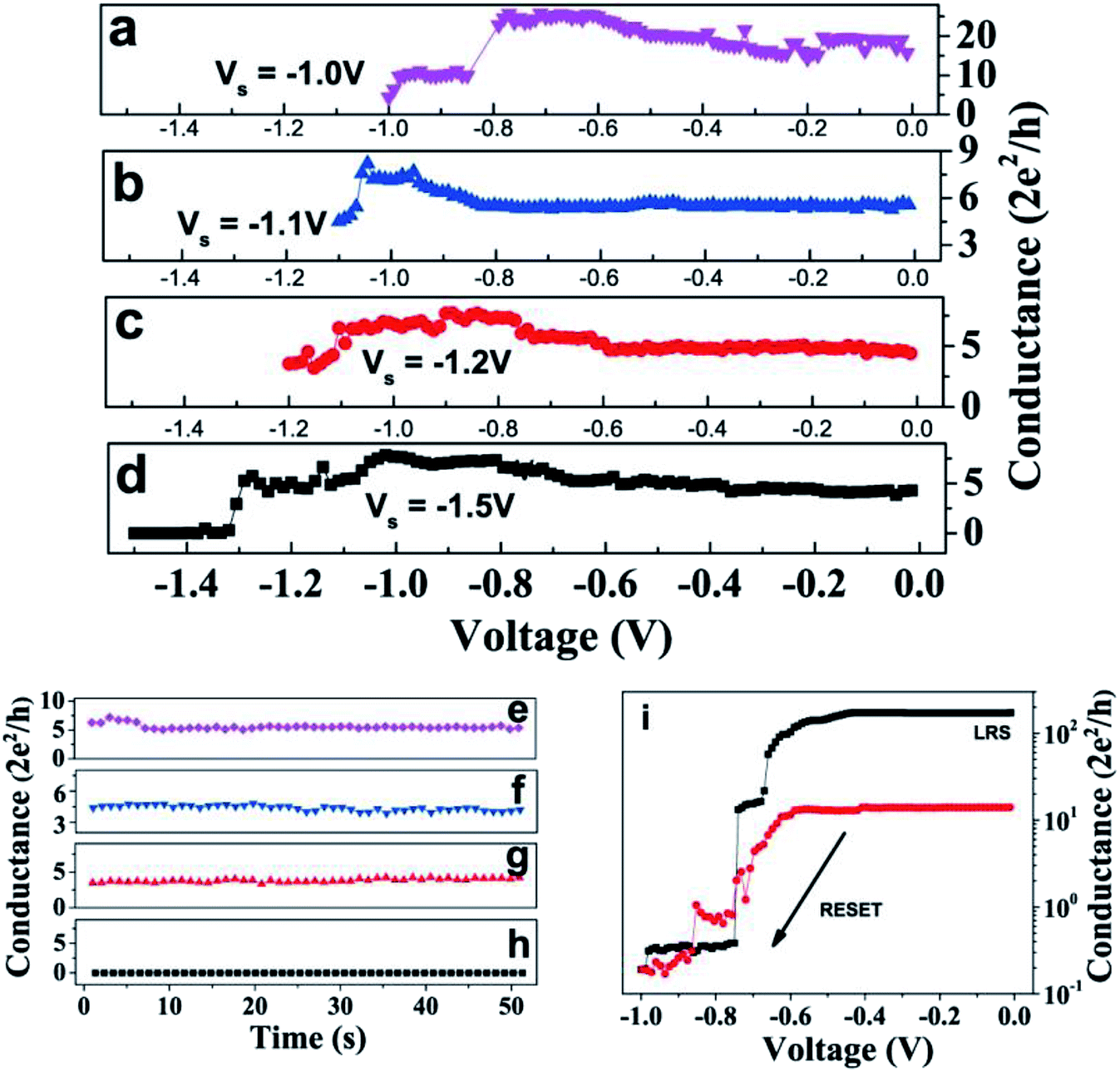 | ||
| Fig. 4 The G–V traces of inter-QC-state switching with successive voltage sweeps during RESET by varying the stop voltages. (a) The device in LRS is switched to ∼6 G0 with stop voltage of Vs = −1.0 V. (b) With of Vs = −1.1 V, a inter-QC-state switching from ∼6 G0 to ∼4.5 G0 is achieved. (c) Subsequently, during voltage sweep with Vs = −1.2 V, QC-state switched to ∼3.5 G0. (d) The figure shows a complete RESET to HRS with Vs = −1.5 V. (e)–(h) The stability with time for final QC-states achieved in figures (a)–(d) are respectively shown. (i) Complete RESET transitions are exhibited. The black trace shows the RESET from LRS to HRS and the red trace shows RESET from ∼15 G0 to HRS state. The complete SET-RESET cycles of traces in (i) is given in the ESI Fig. S5.† | ||
During RESET switching, the critical parameter was the stop-voltage instead of the current compliance limit. For example, during the voltage sweep in Fig. 4a, the conductance starts to decrease or in other words, resistance of the device starts to increase at >−0.8 V. This voltage of −0.8 V becomes important, as, for any stop-voltage chosen little more than −0.8, the device stops at an intermediate stable QC-state, as shown in Fig. 4a–c. However, if stop-voltage is kept sufficiently high, i.e. close to higher end of the RESET voltage range (>−1.0 V), the device will RESET completely, as shown in Fig. 4i. However, this stop-voltage is not a fixed value, as devices have run-to run variations and have a range of voltage for RESET, as it is −0.4 V to −1.2 V for our devices. So, if a device starts to RESET at lower voltage (example: −0.6 V as shown in Fig. 4i), and the stop-voltage is chosen to be −1.0 V, the device RESETs completely earlier than −1.0 V (Fig. 4i), and thus, the device cannot be stopped at any intermediate QC-states. However, if stop-voltage would have been kept in the range −0.7 to −0.8 V for the two RESET traces in Fig. 4i, then the device could, possibly, have stopped at an intermediate QC-state.
Hundreds of inter-QC-state switching events in both SET and RESET directions were performed. The SET and RESET inter-QC-state switching (Fig. 3 and 4) are distinguished by the limiting conditions of current compliance and stop-voltage during voltage sweep cycles, respectively. However, to ensure complete RESET from any QC-state, both current compliance as well as stop-voltage needs to be kept high.
In summary, stable and reproducible QC- states were achieved in Al/Nb2O5/Pt devices by limiting current compliance during the current–voltage measurements. All the states were stable at least for 500 s, and the higher conductance states exhibited longer retention times. The stable quantized states could be controllably switched to higher G0 (SET direction) or to lower G0 (RESET direction) states, by imposing the current compliance or stop-voltage limits, respectively. The conditions for complete RESET, starting from any quantized state, could also be selectively induced by lifting limiting conditions on current or voltage during RESET voltage sweep. The possibility of utilizing the QC-states in the resistive devices for multilevel logic shows potentials for achieving high-density storage.
Conflicts of interest
The authors declare no competing financial interest.Acknowledgements
We would like to thank Dr Karthik Krishnan for helpful discussion. S. D. would like to thank University Grant Commission (UGC) under Senior Research Fellowship (SRF) for financial support. This work was financially supported partly by DST INSPIRE Fellowship and partly by CSIR network project AQuaRIUS (PSC0110).References
- A. Pirovano and K. Schuegraf, Memory Grows Up, Nat. Nanotechnol., 2010, 5, 177 CrossRef CAS PubMed.
- M. H. Lankhorst, B. W. Ketelaars and R. A. Wolters, Low-Cost and Nanoscale Non-Volatile Memory Concept for Future Silicon Chips, Nat. Mater., 2005, 4, 347 CrossRef CAS PubMed.
- R. Waser and M. Aono, Nanoionics-Based Resistive Switching Memories, Nat. Mater., 2007, 6, 833–840 CrossRef CAS PubMed.
- R. Waser, R. Dittmann, G. Staikov and K. Szot, Redox Based Resistive Switching Memories–Nanoionic Mechanisms, Prospects, and Challenges, Adv. Mater., 2009, 21, 2632–2663 CrossRef CAS.
- Y. Li, S. Long, Y. Liu, C. Hu, J. Teng, Q. Liu, H. Lv, J. Suñé and M. Liu, Conductance Quantization in Resistive Random Access Memory, Nanoscale Res. Lett., 2015, 10, 420 CrossRef PubMed.
- F. Lv, K. Ling, W. Wang, P. Chen, F. Liu, W. Kong, C. Zhu, J. Liu and L. Long, Multilevel Resistance Switching Behavior in PbTiO3/Nb:SrTiO3(100) Heterostructure Films Grown by Hydrothermal Epitaxy, J. Alloys Compd., 2019, 778, 768–773 CrossRef CAS.
- L. Wu, J. Guo, W. Zhong, W. Zhang, X. Kang, W. Chen and Y. Du, Flexible, Multilevel, and Low-Operating-Voltage Resistive Memory Based on MoS2–rGO Hybrid, Appl. Surf. Sci., 2019, 463, 947–952 CrossRef CAS.
- J. Xu, X. Zhao, Z. Wang, H. Xu, J. Hu, J. Ma and Y. Liu, Biodegradable Natural Pectin-Based Flexible Multilevel Resistive Switching Memory for Transient Electronics, Small, 2019, 15, 1803970 CrossRef PubMed.
- S. K. Vishwanath, H. Woo and S. Jeon, Enhancement of Resistive Switching Properties in Al2O3 Bilayer-Based Atomic Switches: Multilevel Resistive Switching, Nanotechnology, 2018, 29, 235202 CrossRef PubMed.
- S.-T. Kim and W.-J. Cho, Improvement of Multi-Level Resistive Switching Characteristics in Solution-Processed AlOX -Based Non-Volatile Resistive Memory Using Microwave Irradiation, Semicond. Sci. Technol., 2017, 33, 015009 CrossRef.
- V. K. Nagareddy, M. D. Barnes, F. Zipoli, K. T. Lai, A. M. Alexeev, M. F. Craciun and C. D. Wright, Multilevel Ultrafast Flexible Nanoscale Nonvolatile Hybrid Graphene Oxide–Titanium Oxide Memories, ACS Nano, 2017, 11, 3010–3021 CrossRef CAS PubMed.
- X. Zhao, Z. Fan, H. Xu, Z. Wang, J. Xu, J. Ma and Y. Liu, Reversible Alternation between Bipolar and Unipolar Resistive Switching in Ag/MoS2/Au Structure for Multilevel Flexible Memory, J. Mater. Chem. C, 2018, 6, 7195–7200 RSC.
- P. Hou, Z. Gao and K. Ni, Multilevel Data Storage Memory Based on Polycrystalline SrTiO3 Ultrathin Film, RSC Adv., 2017, 7, 49753–49758 RSC.
- T. Tan, Y. Du, A. Cao, Y. Sun, H. Zhang and G. Zha, Resistive Switching of the HfOx/HfO2 Bilayer Heterostructure and Its Transmission Characteristics as a Synapse, RSC Adv., 2018, 8, 41884–41891 RSC.
- Z.-X. Xu, J.-M. Yan, M. Xu, L. Guo, T.-W. Chen, G.-Y. Gao, Y. Wang, X.-G. Li, H.-S. Luo and R.-K. Zheng, Electric-Field-Controllable Nonvolatile Multilevel Resistance Switching of Bi0.93Sb0.07/PMN-0.29PT(111) Heterostructures, Appl. Phys. Lett., 2018, 113, 223504 CrossRef.
- D. Zhao, I. Katsouras, K. Asadi, W. A. Groen, P. W. M. Blom and D. M. de Leeuw, Retention of Intermediate Polarization States in Ferroelectric Materials Enabling Memories for Multi-Bit Data Storage, Appl. Phys. Lett., 2016, 108, 232907 CrossRef.
- A. K. Tripathi, A. J. J. M. van Breemen, J. Shen, Q. Gao, M. G. Ivan, K. Reimann, E. R. Meinders and G. H. Gelinck, Multilevel Information Storage in Ferroelectric Polymer Memories, Adv. Mater., 2011, 23, 4146–4151 CrossRef CAS PubMed.
- L. Van Lich, T. Shimada, S. Sepideh, J. Wang and T. Kitamura, Multilevel Hysteresis Loop Engineered with Ferroelectric Nano-Metamaterials, Acta Mater., 2017, 125, 202–209 CrossRef CAS.
- J. Wang, K. Nagano, T. Shimada and T. Kitamura, Strain-Mediated Multilevel Ferroelectric Random Access Memory Operating through a Magnetic Field, RSC Adv., 2014, 4, 45382–45388 RSC.
- P. Hou, J. Wang, X. Zhong, Y. Zhang, X. Zhang, C. Tan and B. Li, Voltage Pulse Controlling Multilevel Data Ferroelectric Storage Memory with a Nonepitaxial Ultrathin Film, RSC Adv., 2016, 6, 80011–80016 RSC.
- W. Wu, S. Chen, J. Zhai, X. Liu, T. Lai, S. Song and Z. Song, Multi-Level Storage and Ultra-High Speed of Superlattice-Like Ge50Te50/Ge8Sb92 Thin Film for Phase-Change Memory Application, Nanotechnology, 2017, 28, 405206 CrossRef PubMed.
- A. Athmanathan, M. Stanisavljevic, N. Papandreou, H. Pozidis and E. Eleftheriou, Multilevel-Cell Phase-Change Memory: A Viable Technology, IEEE J. Emerg. Sel. Topics Circuits Syst., 2016, 6, 87–100 Search PubMed.
- Y. Xue, S. Song, S. Yan, T. Guo, Z. Song and S. Feng, Al-Sb-Ge Phase Change Material: A Candidate for Multilevel Data Storage with High-Data Retention and Fast Speed, Scr. Mater., 2018, 157, 152–156 CrossRef CAS.
- K. Jiang, Y. Lu, Z. Li, M. Wang, X. Shen, G. Wang, S. Song and Z. Song, GeTe/Sb4Te Films: A Candidate for Multilevel Phase Change Memory, Mater. Sci. Eng., B, 2018, 231, 81–85 CrossRef CAS.
- Z. Li, Y. Lu, M. Wang, X. Shen, X. Zhang, S. Song and Z. Song, Controllable Multilevel Resistance State of Superlattice-Like GaSb/Ge2Te Films for Ultralong Retention Phase-Change Memory, J. Non-Cryst. Solids, 2018, 481, 110–115 CrossRef.
- S. Long, X. Lian, C. Cagli, X. Cartoixà, R. Rurali, E. Miranda, D. Jiménez, L. Perniola, M. Liu and J. Suñé, Quantum-Size Effects in Hafnium-Oxide Resistive Switching, Appl. Phys. Lett., 2013, 102, 183505 CrossRef.
- S. Tappertzhofen, I. Valov and R. Waser, Quantum Conductance and Switching Kinetics of AgI-Based Microcrossbar Cells, Nanotechnology, 2012, 23, 145703 CrossRef CAS PubMed.
- A. Mehonic, A. Vrajitoarea, S. Cueff, S. Hudziak, H. Howe, C. Labbé, R. Rizk, M. Pepper and A. J. Kenyon, Quantum Conductance in Silicon Oxide Resistive Memory Devices, Sci. Rep., 2013, 3, 2708 CrossRef CAS PubMed.
- T. Hasegawa, K. Terabe, T. Tsuruoka and M. Aono, Atomic Switch: Atom/Ion Movement Controlled Devices for Beyond Von-Neumann Computers, Adv. Mater., 2012, 24, 252–267 CrossRef CAS PubMed.
- X. Zhu, W. Su, Y. Liu, B. Hu, L. Pan, W. Lu, J. Zhang and R.-W. Li, Observation of Conductance Quantization in Oxide-Based Resistive Switching Memory, Adv. Mater., 2012, 24, 3941–3946 CrossRef CAS PubMed.
- S. R. Nandakumar, M. Minvielle, S. Nagar, C. Dubourdieu and B. A. Rajendran, 250 mV Cu/SiO2/W Memristor with Half-Integer Quantum Conductance States, Nano Lett., 2016, 16, 1602–1608 CrossRef CAS PubMed.
- W. Yi, S. E. Savel'Ev, G. Medeiros-Ribeiro, F. Miao, M.-X. Zhang, J. J. Yang, A. M. Bratkovsky and R. S. Williams, Quantized Conductance Coincides with State Instability and Excess Noise in Tantalum Oxide Memristors, Nat. Commun., 2016, 7, 11142 CrossRef CAS PubMed.
- C. Chen, S. Gao, F. Zeng, G. Y. Wang, S. Z. Li, C. Song and F. Pan, Conductance Quantization in Oxygen-Anion-Migration-Based Resistive Switching Memory Devices, Appl. Phys. Lett., 2013, 103, 043510 CrossRef.
- S. Deswal, A. Kumar and A. Kumar, Investigating Unipolar Switching in Niobium Oxide Resistive Switches: Correlating Quantized Conductance and Mechanism, AIP Adv., 2018, 8, 085014 CrossRef.
- A. Fekadu Gochole, W. Jiyong, S. Jeonghwan, P. Jaehyuk, L. Seokjae, S. Changhyuck and H. Hyunsang, Controllable Quantized Conductance for Multilevel Data Storage Applications Using Conductive Bridge Random Access Memory, Nanotechnology, 2017, 28, 115707 CrossRef PubMed.
- B. C. Jang, S. Kim, S. Y. Yang, J. Park, J.-H. Cha, J. Oh, J. Choi, S. G. Im, V. P. Dravid and S.-Y. Choi, Polymer Analog Memristive Synapse with Atomic-Scale Conductive Filament for Flexible Neuromorphic Computing System, Nano Lett., 2019, 19, 839–849 CrossRef PubMed.
- K. Krishnan, M. Muruganathan, T. Tsuruoka, H. Mizuta and M. Aono, Highly Reproducible and Regulated Conductance Quantization in a Polymer-Based Atomic Switch, Adv. Funct. Mater., 2017, 27, 1605104 CrossRef.
- K. Terabe, T. Hasegawa, T. Nakayama and M. Aono, Quantized Conductance Atomic Switch, Nature, 2005, 433, 47–50 CrossRef CAS PubMed.
- Q. Wang, R. Liu, D. Xiang, M. Sun, Z. Zhao, L. Sun, T. Mei, P. Wu, H. Liu, X. Guo, Z.-L. Li and T. Lee, Single-Atom Switches and Single-Atom Gaps Using Stretched Metal Nanowires, ACS Nano, 2016, 10, 9695–9702 CrossRef CAS PubMed.
- S.-Y. Wang, C.-W. Huang, D.-Y. Lee, T.-Y. Tseng and T.-C. Chang, Multilevel Resistive Switching in Ti/CuxO/Pt Memory Devices, J. Appl. Phys., 2010, 108, 114110 CrossRef.
- C. Hu, M. D. McDaniel, A. Posadas, A. A. Demkov, J. G. Ekerdt and E. T. Yu, Highly Controllable and Stable Quantized Conductance and Resistive Switching Mechanism in Single-Crystal TiO2 Resistive Memory on Silicon, Nano Lett., 2014, 14, 4360–4367 CrossRef CAS PubMed.
- Y. Sharma, P. Misra, S. P. Pavunny and R. S. Katiyar, Multilevel Unipolar Resistive Memory Switching in Amorphous SmGdO3 Thin Film, Appl. Phys. Lett., 2014, 104, 073501 CrossRef.
- C.-H. Hsu, Y.-S. Fan and P.-T. Liu, Multilevel Resistive Switching Memory with Amorphous InGaZnO-Based Thin Film, Appl. Phys. Lett., 2013, 102, 062905 CrossRef.
Footnote |
| † Electronic supplementary information (ESI) available: Additional details on device fabrication, switching characteristics and stability; the inter-quantized-state switching in SET as well as in RESET directions. See DOI: 10.1039/c9ra00726a |
| This journal is © The Royal Society of Chemistry 2019 |