
 Open Access Article
 This Open Access Article is licensed under a Creative Commons Attribution-Non Commercial 3.0 Unported Licence
Synthesis of Mg and Zn diolates and their use in metal oxide deposition†‡
Peter Frenzela,
Andrea Preußa,
Jörn Bankwitzb,
Colin Georgib,
Fabian Ganssd,
Lutz Mertensf,
Stefan E. Schulzbc,
Olav Hellwigde,
Michael Mehring f and
Heinrich Lang*a
f and
Heinrich Lang*a
aTechnische Universität Chemnitz, Faculty of Natural Sciences, Institute of Chemistry, Inorganic Chemistry, D-09107 Chemnitz, Germany. E-mail: heinrich.lang@chemie.tu-chemnitz.de; Fax: +49(0)371-531-21219; Tel: +49(0)371-531-21210
bFraunhofer Institute for Electronic Nano Systems (ENAS), Technologie-Campus 3, D-09126 Chemnitz, Germany
cTechnische Universität Chemnitz, Center for Microtechnologies, D-09107 Chemnitz, Germany
dTechnische Universität Chemnitz, Faculty of Natural Sciences, Institute of Physics, D-09107 Chemnitz, Germany
eHelmholtz-Zentrum Dresden-Rossendorf, Institute of Ion Beam Physics and Materials Research, D-01328 Dresden, Germany
fTechnische Universität Chemnitz, Faculty of Natural Sciences, Institute of Chemistry, Coordination Chemistry, D-09107 Chemnitz, Germany
First published on 5th April 2019
Abstract
The synthesis of complexes [M(OCHMeCH2NMeCH2)2] (5, M = Mg; 7, M = Zn) is described. Treatment of MeHNCH2CH2NMeH (1) with 2-methyloxirane (2) gave diol (HOCHMeCH2NMeCH2)2 (3), which upon reaction with equimolar amounts of MR2 (4, M = Mg, R = Bu; 6, M = Zn, R = Et) gave 5 and 7. The thermal behavior and vapor pressure of 5 and 7 were investigated to show whether they are suited as CVD (= chemical vapor deposition) and/or spin-coating precursors for MgO or ZnO layer formation. Thermogravimetric (TG) studies revealed that 5 and 7 decompose between 80–530 °C forming MgO and ZnO as evidenced by PXRD studies. In addition, TG-MS-coupled experiments were carried out with 7 proving that decomposition occurs by M–O, C–O, C–N and C–C bond cleavages, as evidenced from the detection of fragments such as CH4N+, C2H4N+, C2H5N+, CH2O+, C2H2O+ and C2H3O+. The vapor pressure of 7 was measured at 10.4 mbar at 160 °C, while 5 is non-volatile. The layers obtained by CVD are dense and conformal with a somewhat granulated surface morphology as evidenced by SEM studies. In addition, spin–coating experiments using 5 and 7 as precursors were applied. The corresponding MO layer thicknesses are between 7–140 nm (CVD) or 80 nm and 65 nm (5, 7; spin-coating). EDX and XPS measurements confirm the formation of MgO and ZnO films, however, containing 12–24 mol% (CVD) or 5–9 mol% (spin-coating) carbon. GIXRD studies verify the crystalline character of the deposited layers obtained by CVD and the spin-coating processes.
Introduction
Recently, magnesium and zinc oxide have received great attention, since they possess a broad range of chemical and physical properties. For example, ZnO is an n-type semiconductor (band gap ∼3.3 eV), which shows piezoelectric characteristics, making it attractive for its use as thin films in solar cells,1,2 transparent transistors,3–5 and nano-generators for low frequency applications.6 In addition, ZnO represents an interesting alternative as a transparent electrode for commonly used ITO (indium-doped tin oxide), due to its low absorption in the UV range, high availability, low-cost and non-toxicity.7,8 Another application of ZnO includes its use as a gas sensor.9–11Magnesium oxide is a promising candidate for the generation of thin films of inorganic high-κ metal oxide dielectrics, due to its wide band gap (7.8 eV), low refractive index (1.72), low dielectric constant (9.8), high melting point (2900 °C), chemical and thermal stability, as well as its outstanding diffusion barrier properties.12–16 Moreover, MgO thin films can be used for the protection of plasma display panels from erosion by ion bombardment.17
Several deposition methodologies for MgO and ZnO layer formation exist, including the sol–gel process in combination with spin-coating,18,19 spray pyrolysis,20,21 pulsed laser deposition,22,23 molecular beam epitaxy,24 as well as metal–organic gas phase deposition techniques such as CVD (= chemical vapor deposition)25–27 and ALD (= atomic layer deposition).28,29 Among them, CVD and spin-coating provide convincing alternatives owing to their simplicity of processing control, covering of large areas and their capability to allow adherent and reproduceable films at low cost.30–33
For ZnO film formation diverse zinc complexes such as diethylzinc,34–36 zinc acetates,37,38 alkylzinc alkoxides,39 zinc β-ketoiminates,27,40 zinc β-iminoesterates32,40 and zinc acetylacetonates41,42 are used as CVD precursors. While zinc acetate,37,38 alkylzinc alkoxide39 and zinc β-ketoiminate40 complexes give ZnO without any addition of a co-reactant, ZnEt2 requires, however, oxygen as reactive gas to produce ZnO.34–36 However, the pyrophoric nature and reactivity impedes its easy handling. In addition, ZnEt2 shows undesired pre-reactions and hence decomposition by the deposition of particulates, upstream from the heating element may occur during the precursor delivery.32,39,43
For MgO film formation, bis(cyclopentadienyl) magnesium,25,44 alkylmagnesium alkoxides,45,46 magnesium carboxylates,47,48 magnesium β-ketoiminates,49 magnesium β-diketonates26 and their diamine adducts12,50,51 are usually used as CVD precursors of which the latter ones are promising CVD candidates, due to their high volatility, good stability in the condensed and gas phase, and their straightforward synthetic procedure.12,50,51
In contrast, as spin-coating precursors mainly magnesium acetate tetrahydrate or zinc acetate dihydrate were used for the formation of the respective metal oxide layers.52,53 In addition, also MgO/ZnO composite materials are accessible.54 In combination with copper(II) acetate monohydrate CuO/ZnO layers can be obtained.55
Herein, we describe the synthesis of magnesium and zinc diolates [M(OCHMeCH2NMeCH2)2] (M = Mg, Zn). Their thermal decomposition behavior and their use as spin-coating (Mg, Zn) and CVD (Zn) precursors for metal oxide deposition on Si/SiO2 substrates is discussed.
Experimental
General
Reactions for the synthesis of 5 and 7 were carried out under an atmosphere of argon using anhydrous and degassed solvents. Hexane (95%, Grüssing) was purified by distillation from NaH. Ethanol (>99%, Acros Organics) was distilled from sodium/diethyl phthalate. 2-Methoxyethanol (98%, abcr) was purified by distillation from CaH2. All other chemicals 2-methyloxirane (≥99.5%, Merck), N,N′-dimethylethylenediamine (>95%, ChemPur), methanol (>99%, Acros Organics), 0.5 M solution of MgBu2 in heptane (Acros Oranics), 1.0 M solution of ZnEt2 in hexane (Merck) were purchased from commercial suppliers and were used without any further purification.Instruments
NMR spectra (500.3 MHz for 1H, 125.8 MHz for 13C{1H}) were recorded using a Bruker Avance III 500 FT-NMR spectrometer at ambient temperature. Chemical shifts are reported in ppm downfield from tetramethylsilane with the solvent as reference signal (1H NMR, δ CDCl3 7.26 ppm, C6D6 7.16 ppm; 13C{1H} NMR, δ CDCl3 77.16 ppm, C6D6 128.06 ppm). Infrared spectra were recorded with a Thermo Nicolet 200 FT-IR spectrometer. Elemental analyses were performed with a Thermo FLASHEA 1112 Series instrument. High-resolution mass spectra were recorded with a Bruker Daltonik micrOTOF-QII mass spectrometer performing in the ESI mode. The melting points were determined by using a Gallenkamp MFB 595 010 M melting point apparatus. Vapor pressure measurements were performed with a Mettler Toledo TGA/DSC1 1100 system with a UMX1 balance. The TG and TG-MS experiments were performed with a Mettler Toledo TGA/DSC1 1600 system with a MX1 balance coupled with a Pfeifer Vacuum MS Thermostar GSD 301 T2 mass spectrometer. PXRD measurements of the respective TG residues were performed with a STOE-STADI P diffractometer equipped with a Ge(111) monochromator and CuKα radiation (λ = 1.540598 Å, 40 kV, 40 mA). The crystallite size was estimated according to the Scherrer equation: τ = Kλ/β![[thin space (1/6-em)]](https://www.rsc.org/images/entities/char_2009.gif) cosθ, where τ is the volume weighted crystallite size, K is the Scherrer constant (here taken as 1.0), λ is the X-ray wavelength, θ is the Bragg angle in °. Theta, and β is the full width of the diffraction line at half of the maximum intensity (fwhm, background subtracted). The fwhm is corrected for instrumental broadening using a LaB6 standard (SRM 660) purchased from NIST. The value of β was corrected from (β2measured and β2instrument are the fwhm's of measured and standard profiles): β2 = β2measured − β2instrument. Spin-coating experiments were carried out with a spin coater system WS-650MZ-23NPP/A1/AR1. For CVD experiments a home-built vertical cold-wall CVD reactor with heater dimension of 20 × 20 mm (BACH Resistor Ceramics GmbH) was used (for more details see ref. 56). Heating could be adjusted up to 500 °C and was controlled by a Gefran 600 module connected with a Pt100 thermosensor. The flow rates of carrier gas (N2) and the reactive gas (O2) were controlled by MKS type 247 mass flow controllers connected to the reactor by heated copper lines. The CVD system was attached to a rotary vane pump RZ 6 (Vacuubrand). The pressure of the reactor system was controlled by a Vacuubrand vacuum controller (CVC 3000) in combination with an external Pirani vacuum sensor (VSP 3000).
cosθ, where τ is the volume weighted crystallite size, K is the Scherrer constant (here taken as 1.0), λ is the X-ray wavelength, θ is the Bragg angle in °. Theta, and β is the full width of the diffraction line at half of the maximum intensity (fwhm, background subtracted). The fwhm is corrected for instrumental broadening using a LaB6 standard (SRM 660) purchased from NIST. The value of β was corrected from (β2measured and β2instrument are the fwhm's of measured and standard profiles): β2 = β2measured − β2instrument. Spin-coating experiments were carried out with a spin coater system WS-650MZ-23NPP/A1/AR1. For CVD experiments a home-built vertical cold-wall CVD reactor with heater dimension of 20 × 20 mm (BACH Resistor Ceramics GmbH) was used (for more details see ref. 56). Heating could be adjusted up to 500 °C and was controlled by a Gefran 600 module connected with a Pt100 thermosensor. The flow rates of carrier gas (N2) and the reactive gas (O2) were controlled by MKS type 247 mass flow controllers connected to the reactor by heated copper lines. The CVD system was attached to a rotary vane pump RZ 6 (Vacuubrand). The pressure of the reactor system was controlled by a Vacuubrand vacuum controller (CVC 3000) in combination with an external Pirani vacuum sensor (VSP 3000).
The surface morphology was investigated by field-emission scanning electron microscopy using a ZEISS Supra60 SEM with an accelerating voltage of 2 or 3 kV. Cross-sectional SEM investigations were carried out to determine the film thickness. Energy-dispersive X-ray analysis using a Bruker Quantax 400 system attached to a SEM was applied to determine the chemical composition of the films. The composition of the samples were investigated using a PREVAC XPS system. Monochromatic aluminum Kα radiation (1486.6 eV) was provided by a VG Scienta MX 650 X-ray source and a monochromator. The energy distribution of the photoelectrons was measured using a VG Scienta EW3000 analyzer. This analyzer was operated at 200 eV pass energy with a step size of 200 meV and a measurement time of 2.0 s for each data point for detailed spectra, and 1 eV step size and 1.0 s measurement time at each point for survey spectra. The Casa XPS 2.3.16 Pre-rel 1.4 software was used for the deconvolution of the XPS peaks. For the calculation of the atomic concentration, Scofield relative sensitivity factors (RSFs) were used. These RSFs were corrected for a monochromator-analyzer angle of 52.55°. For the escape depth correction in Casa XPS, a value of −0.75 was applied. GIXRD (= grazing incidence X-ray diffraction) measurements of the CVD and spin-coated films have been carried out with a Rigaku SmartLab 9 kW diffractometer using a parallel beam of Cu Kα radiation. The source was operated at 45 kV and 200 mA. The incidence angle was set to 0.32° for the ZnO films and to 0.25° for the MgO layer in order to maximize the reflex intensity of the thin films and only the detector axis was moved to perform the 2θ scans. The samples have been rotated within the film plane to an offset of approximately 5° so that any reflexes from the single-crystalline silicon substrate were mostly suppressed. The incident beam was limited to 5 mm × 0.1 mm and the detector was equipped with a parallel slit analyzer. The integration time per data point was set to 1.5 s for the layers C and D, 6 s for the other layers.
Synthesis of 3,3′-N,N′-dimethylethylenediaminodipropan-2,2′-diol (3)
N,N′-Dimethylethylenediamine (1) (12 mL, 112 mmol) was dissolved in 40 mL of methanol at ambient temperature and this solution was cooled down to 0 °C. To this solution 2-methyloxirane (21.1 mL, 302 mmol) (2) was added within 30 min. Stirring of the reaction mixture was continued for 7 h at 0 °C. Subsequently, the reaction mixture was warmed-up to ambient temperature and was then stirred for further 7 h at this temperature. After evaporation of all volatiles in vacuum, the obtained crude product was purified by distillation (85 °C, 5 × 10⁻² mbar). The title compound was obtained as a mixture of two diastereomers as a colorless oil. Yield: 20.6 g (101 mmol, 90% based on 1).Anal. calcd for C10H24N2O2 (204.31 g mol−1): C, 58.79; H, 11.84; N, 13.71. Found: C, 58.70; H 11.65; N, 13.70. Bp: 85 °C at 5 × 10⁻² mbar. IR (CHCl3, NaCl; cm−1): 3400 (br), 2974 (vs), 2849 (vs), 2804 (vs), 1455 (vs), 1413 (m), 1377 (m), 1356 (m), 1331 (s), 1299 (s), 1136 (s), 1067 (vs), 1034 (vs), 956 (s), 843 (s), 772 (vs). 1H NMR§ (CDCl3, δ): 4.79 (s, br, 4H, OH), 3.75–3.83 (m, 4H, CH), 2.61–2.68 (m, 2H, CH2), 2.44–2.55 (m, 4H, CH2), 2.20–2.32 (m, 22H, CH3, CH2), 1.06 (d, 3JHH = 6.20 Hz, 6H, CH3), 1.05 (d, 3JHH = 6.20 Hz, 6H, CH3). 13C{1H} NMR§ (CDCl3, δ): 65.29 (CH2), 64.86 (CH2), 64.29 (CH), 64.17 (CH), 55.82 (CH2), 54.70 (CH2), 43.77 (CH3), 43.11 (CH3), 20.07 (CH3), 20.01 (CH3). HRMS (ESI-TOF, m/z): calcd for C10H25N2O2 [M + H]+: 205.1911, found 205.1954.
Synthesis of magnesium and zinc diolates 5 and 7
Anal. calcd for C10H22MgN2O2 (226.60 g mol−1): C, 53.00; H, 9.79; N, 12.36. Found: C, 53.11; H 10.05; N, 12.30. Mp: 100 °C decomposition. IR (KBr; cm−1): 2965 (vs), 2848 (vs), 2803 (vs), 2652 (w), 2595 (w), 1459 (s), 1421 (w), 1359 (m), 1315 (m), 1296 (m), 1209 (w), 1165 (s), 1135 (s), 1094 (s), 1065 (vs), 1031 (s), 985 (s), 962 (m), 943 (m), 864 (w), 806 (w), 618 (m), 572 (s), 514 (m). 1H NMR (CDCl3, δ): 4.3–0.7 (m, CH, CH2, CH3). 13C{1H} NMR (CDCl3, δ): see the ESI. HRMS (ESI-TOF, m/z): calcd for C10H23MgN2O2 [M + H]+: 227.1604, found 227.1690.
Anal. calcd for C10H22N2O2Zn (267.67 g mol−1): C, 44.87; H, 8.28; N, 10.47. Found: C, 44.46; H 8.55; N, 10.15. Mp: 160 °C decomposition. IR (KBr; cm−1): 2965 (vs), 2911 (vs), 2847 (vs), 2571 (m), 1467 (s), 1457 (s), 1355 (s), 1338 (m), 1328 (m), 1312 (s), 1272 (w), 1206 (w), 1187 (w), 1136 (vs), 1088 (vs), 1073 (vs), 1048 (s), 978 (vs), 964 (s), 923 (s), 853 (s), 826 (m), 794 (m), 608 (m), 581 (s), 513 (s). 1H NMR (C6D6, δ): 4.5–0.6 (m, CH, CH2, CH3). 13C{1H} NMR (C6D6, δ): see the ESI. HRMS (ESI-TOF, m/z): calcd for C10H23N2O2Zn [M + H]+: 267.1046, found 267.1045.
Spin-coating experiments
For the spin-coating experiments 2 mL of a 0.5 M solution of 5 (227 mg, 1 mmol) in 2-methoxyethanol or 2 mL of a 0.5 M solution of 7 (268 mg, 1 mmol) in ethanol was prepared. For the deposition experiments 0.17 mL of the solution containing 5 or 0.22 mL of the solution containing 7 were used. The respective substrates of size 20 mm × 20 mm were cleaned with ethanol by bath sonication and were afterwards air dried at ambient temperature.Results and discussion
The synthesis of the magnesium and zinc diolates [M(OCHMeCH2NMeCH2)2] (5, M = Mg; 7, M = Zn) is outlined in Scheme 1. The therefore necessary chelate (HOCHMeCH2NMeCH2)2 (3) is available as a mixture of two diastereomers by the reaction of N,N′-dimethylethylenediamine (1) with 2.7 equiv. of 2-methyloxirane (2) in methanol at ambient temperature. Treatment of 3 with equimolar amounts of MR2 (4, M = Mg, R = Bu; 6, M = Zn, R = Et) gave coordination complexes 5 and 7, respectively, along with RH (Scheme 1). Both complexes were obtained as colorless solids, which poorly dissolve in solvents such as toluene, chloroform, methanol and tetrahydrofuran, while in 2-methoxyethanol or ethanol they show good solubility. Exposure of such solutions to air and moisture resulted in the decomposition of 5 (within 1 h) and 7 (15 min). Hence, it is advisable, to store these complexes under an atmosphere of inert gas.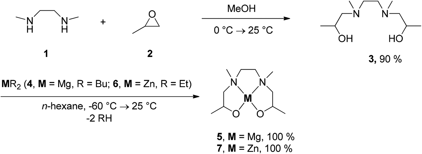 | ||
| Scheme 1 Synthesis of coordination complexes 5 and 7 via 3. | ||
Compounds 3, 5 and 7 were characterized by elemental analysis, IR and NMR (1H, 13C{1H}) spectroscopy and high-resolution ESI-TOF mass-spectrometry (Experimental). Additionally, the thermal behavior of 5 and 7 was studied by thermogravimetry (TG) and TG-coupled mass-spectrometry (TG-MS) (7). In addition, the vapor pressure of 7 was determined.
In the 13C{1H} NMR spectrum of 3 two sets of resonance signals can be observed due to its diastereomeric character (Experimental). Upon the reaction of 3 with 4 and 6, respectively, the 1H and 13C{1H} NMR spectra become more complex due to the formation of different isomers (see the ESI‡), an assignment of signals was not possible.
Characteristic in the IR spectrum of 3 is the appearance of the ![[small upsilon, Greek, tilde]](https://www.rsc.org/images/entities/char_e131.gif) (OH) vibration at 3400 cm−1, which disappears upon complexation to M (M = Mg, Zn). Hence, IR spectroscopy is suitable to monitor the reaction of 3 with 4 and 6 to give 5 and 7.
(OH) vibration at 3400 cm−1, which disappears upon complexation to M (M = Mg, Zn). Hence, IR spectroscopy is suitable to monitor the reaction of 3 with 4 and 6 to give 5 and 7.
In the ESI-TOF mass-spectra the protonated molecular ion peaks [M + H]+ could be detected at m/z = 205.1954 for 3, 227.1690 for 5 and 267.1045 for 7.
Thermal behavior
To gain first information about the thermal behavior of 5 and 7 thermogravimetric measurements were carried out both in an atmosphere of argon (gas flow 20 mL min−1) and oxygen (gas flow 20 mL min−1) in the temperature range of 40–800 °C with a heating rate of 10 °C min−1. Additionally, a continuous argon carrier gas flow of 40 mL min−1 was used for all measurements. The TG traces from the measurements in argon and oxygen are depicted in Fig. 1. As it can be seen from this figure, complexes 5 and 7 decompose under oxygen within the temperature range of 80–530 °C (Fig. 1, left), while under an atmosphere of argon decomposition occurs between 100–480 °C (Fig. 1, right). Residual masses of 18.2% (5, O2) or 17.4% (5, Ar) and 30.1% (7, O2) were recorded at 800 °C, which are close to the theoretical residual mass of MgO (17.8%) and ZnO (30.4%) (Table 1). However, under an atmosphere of argon a residual mass of 22.1% was observed for 7, owing to the fact that it partially evaporates during the heating process.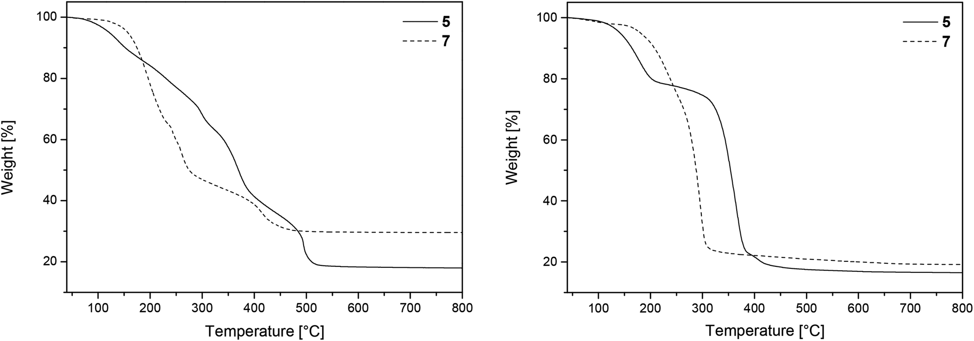 | ||
| Fig. 1 TG traces of 5 and 7 under an atmosphere of oxygen (left) and argon (right) (gas flow 20 mL min−1, heating rate 10 °C min−1). | ||
| Compd. | Decomp. range (Ar) [°C] | Decomp. range (O2) [°C] | Calcd MO content [%] | TG residue (Ar) [%] | TG residue (O2) [%] |
|---|---|---|---|---|---|
| a Decomp. = decomposition; MO = metal oxide. | |||||
| 5 | 100–480 | 80–530 | 17.8 | 17.4 | 18.2 |
| 7 | 160–400 | 120–490 | 30.4 | 22.1 | 30.1 |
Powder X-ray diffraction (PXRD) measurements of the residues obtained after TG confirmed the formation of crystalline MgO (complex 5) [ICDD 00-045-0946] and ZnO (7) [ICDD 01-070-8070], respectively (Fig. 2). The related crystallite sizes were calculated by using the Scherrer equation (Experimental). The estimation reveals crystallite sizes of 11 ± 1 nm for 5 and 43 ± 5 for 7, respectively.
 | ||
| Fig. 2 PXRD patterns of the TG residues of 5 (left) and 7 (right) under oxygen, showing the characteristic reflections (red) of crystalline MgO and ZnO (crystal size: 11 ± 1 nm (left) and 43 ± 5 nm (right)). | ||
In addition, TG-MS studies were carried out on the example of 7 in order to get a deeper insight into the decomposition behavior of this species. The appropriate TG-MS traces including the TG trace, its first derivative and the respective mass-to-charge ratios (m/z) are depicted in Fig. 3. It is concluded that between 120 °C and 230 °C a partial evaporation and decomposition of 7 occurs, resulting in a weight loss of 25.3%. The fragments detected are of low intensity. The 2nd decomposition step (230–400 °C) illustrates an overall weight loss of 52.8% with m/z fragments of higher intensity (Fig. 3). As characteristic ions, CH3+ (m/z = 15), C2H2+/CN+ (26), C2H3+/HCN+ (27), C2H5+/CHO+ (29), CH4N+/CH2O+ (30), C2H4N+/C2H2O+ (42) and C2H5N+/C2H3O+ (43) could be detected, indicating the cleavage of Zn–O, N–C and C–C bonds.
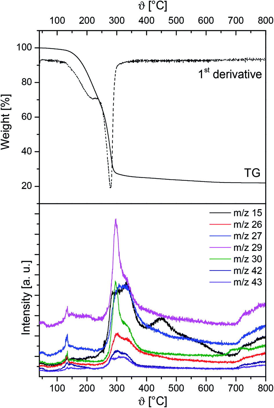 | ||
| Fig. 3 TG trace and the 1st derivative (top) and TG-MS traces (bottom) of 7 (atmosphere of argon, gas flow 20 mL min−1; heating rate 5 °C min−1; (m/z 15 (CH3+), 26 (C2H2+, CN+), 27 (C2H3+, HCN+), 29 (C2H5+, CHO+) 30 (CH4N+, CH2O+), 42 (C2H4N+, C2H2O+) and 43 (C2H5N+, C2H3O+))). | ||
Vapor pressure measurements
Vapor pressure measurements were carried out to prove, if 5 and 7 are suited to be used as CVD precursors for the deposition of MO layers (M = Mg, Zn). The methodology used within this work is based on the mass loss of the samples as a function of increasing temperature at atmospheric pressure (Experimental). Therefore, a TG system with a horizontal balance was applied to determine the weight loss in an isothermal phase at different temperatures as described previously.56 To minimize the measurement errors and provide reliable experimental data, each study was carried out thrice. It was found that 5 is non-volatile and hence was solely used in the deposition of MgO by applying the spin-coating process (see below). In contrast, complex 7 is volatile. The temperature range was set to 120–220 °C according to the TG study (Fig. 1) to avoid decomposition during the vapor pressure investigation of 7. The linear regression of the data giving the characteristic Antoine parameters A and B for 7 according to the Antoine eqn (1) are summarized in Table 2.|
logp = A − B/T
| (1) |
To compare the volatility of 7 with literature known systems, zinc chelate complexes such as the fluorinated zinc acetylacetonate [Zn{CF3C(O)CHC(O)CH3}2]57 and the zinc β-ketoiminate [Zn{CF3C(O)CHC(NH(CH2)2OMe)Me}2]58 have been used as reference compounds. It should be noticed that there is a lack of vapor pressure measurements for the zinc chelate compounds, despite of their wide use in the numerous applications for deposition of ZnO. Complex 7 possesses a vapor pressure of 10.4 mbar at 160 °C (Fig. 4). This value is comparable with the one for [Zn{CF3C(O)CHC(O)CH3}2] (140 °C of 11.1 mbar)57 but significantly higher than the vapor pressure for [Zn{CF3C(O)CHC(NH(CH2)2OMe)Me}2] (0.53 mbar at 160 °C).58 Hence, complex 7 was investigated for its applicability in the low pressure CVD process (see below).
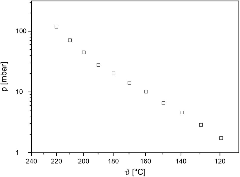 | ||
| Fig. 4 Vapor pressure trace of 7 in an atmosphere of nitrogen (40 mL min−1). | ||
Chemical vapor deposition
Chemical vapor deposition experiments using 7 as CVD precursor were performed in a home-built vertical cold-wall CVD reactor equipped with a continuous evaporation system.56 The deposition studies were conducted using nitrogen (gas flow 60 mL min−1) as carrier gas and oxygen (gas flow 20 mL min−1 and 60 mL min−1) as reactive gas (Experimental). As substrate, silicon wafers (20 × 20 mm) covered with a native oxide layer were applied. Prior to the deposition experiments the substrates were cleaned with ethanol and were dried at ambient temperature. The applied deposition conditions are summarized in Table 3.In a typical deposition experiment, precursor 7 was heated to 165 °C in the CVD vaporizer unit under a pressure of 1.1–1.7 mbar (Table 3). The reactor walls were additionally heated (100 °C) to achieve a continuous precursor flow rate. According to TG studies (Fig. 1) the substrate temperature was set to 250 °C and thereafter was increased stepwise up to 450 °C producing layers A–D (Table S1, see the ESI‡). For all CVD studies the deposition time was adjusted to 45 min for a better comparison of evaporation and growth rates. To the carrier gas different ratios of the reactive gas oxygen (N2:O2 = 1:1, 3:1) were added (Table 3). Under all applied deposition conditions, the formation of thin zinc oxide layers was observed. The morphology and layer thicknesses of the as-deposited films were determined by Scanning Electron Microscopy (SEM). It was found that the reactive gas flow rate and the substrate temperature strongly influence the growth rate and hence the layer formation. The obtained layers are dense and conformal with a granulated surface morphology with layer thicknesses up to 140 nm (Table 3). The thinner films are metallic silver colored, whereas thicker films possess a golden or bluish metallic appearance.
Layer characterization
The morphology and chemical composition of the as-deposited ZnO layers were studied by using SEM, EDX (= energy-dispersive X-ray spectroscopy), XPS (= X-ray photoelectron spectroscopy) and GIXRD (= grazing incidence X-ray diffraction). From Fig. 5 it can be seen that all obtained ZnO layers (A–D) are dense and conformal. Above all, layers B–D show a granulated topography.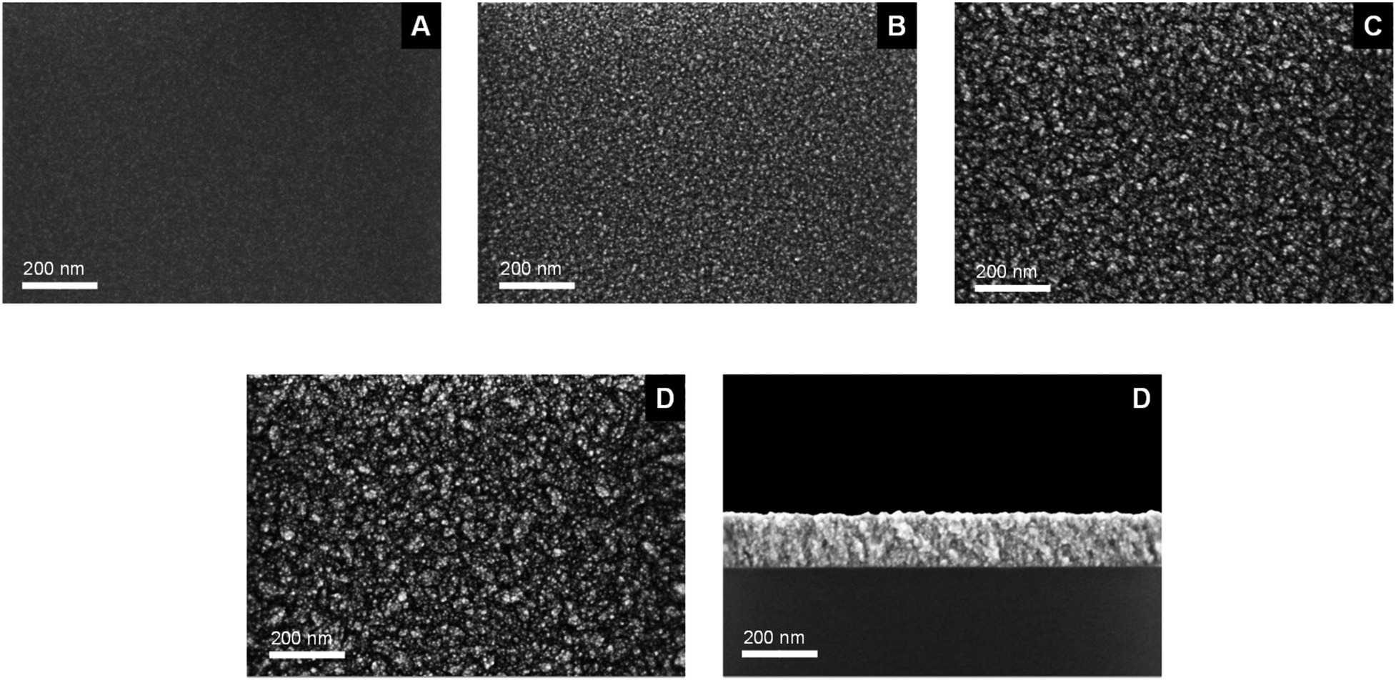 | ||
| Fig. 5 SEM images of as-deposited layers A–D and a cross-sectional image (bottom right) of layer D using 7 as CVD precursor, deposited on Si/SiO2 substrates (for layer composition see Table 4). | ||
The layer thicknesses of the respective films were determined to 7 nm (A), 8 nm (B), 65 nm (C) and 140 nm (D) from cross-sectional SEM images (Table 3). Exemplary, the cross sectional view of layer D is shown in Fig. 5, whereas all other images are presented in Fig. S1–S4 (see the ESI‡). Layers A and B show similar film thicknesses and hence equal growth rates, though the deposition temperature for the formation of layer B is 80 °C higher than for A, but the higher applied temperature effects more granulated surface morphologies (layer B). A significant increase of the growth rate was achieved, when the gas flow rate of oxygen was enhanced from 20 mL min−1 to 60 mL min−1 as evidenced for layer C (1.5 nm min−1; for comparison 0.2 nm min−1 B). The deposition rate of 7 could be further increased to 3.1 nm min−1 by applying a higher substrate temperature of 450 °C.
The film composition of the as-deposited layers A–D was analysed by EDX spectroscopy using different electron beam energies, showing a similar pattern of zinc and oxygen signals for all films. Representative, the EDX spectrum of layer A is depicted in Fig. 6, whereas all other EDX spectra of the layers A–D (Fig. S5–S8) are shown in the ESI.‡
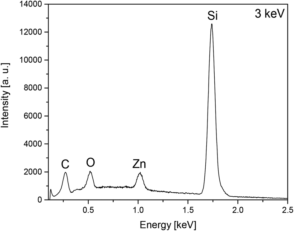 | ||
| Fig. 6 EDX spectra of layer A obtained from 7 by CVD showing the characteristic pattern of zinc and the presence of oxygen, carbon and silicon by using an electron beam energy of 3 keV. | ||
Moreover, carbon and silicon could be detected. In spite of low electron beam energy (3 keV) the signal intensity for Si of the A and B films is very high, ascribing to excitation of the substrate material, due to the thin film thickness of the as-deposited layers. Contrastingly, EDX spectra of thicker layers (C and D) show no or signals of rather low intensity.
In order to determine the film composition without penetration of the underlying native SiO2 layer and silicon wafer, surface sensitive ex situ XPS measurements were performed. All XPS measurements were carried out on the respective ZnO surfaces and in the layers (Fig. 7 and S11–S14 (ESI); Tables 4 and S1 (ESI)‡). Since XPS is a surface sensitive measurement method, contaminations on the surface may be overestimated, therefore, the airborne hydrocarbon impurities and carbon surface contaminations of precursor molecules on the topmost layer have been removed by argon ion sputtering (4 keV, 5 mA current at an angle of 60° with respect to the sample plane, 5 min, 2 × 2 mm2 sputtering field). Concentration quantification was achieved by using standard single element sensitivity factors.59 The Zn 2p3/2, O 1s and C 1s peaks appearing at 1021.2 eV, 529.6 eV and 284.6 eV were used to calculate the chemical composition.
 | ||
| Fig. 7 Ex situ XPS spectra of the ZnO layer C obtained from 7 at 400 °C (N2, 60 mL min−1, O2, 60 mL min−1, after 5 min sputtering, Ar+, 4 keV). | ||
The XPS measurements of the layers confirm the presence of zinc, oxygen and carbon in the deposited films. The typical XPS spectrum of the ZnO layer C deposited at 400 °C and the corresponding detailed XPS spectra of Zn 2p3/2, O 1s and C 1s after the sputtering process (5 min, Ar+, 4 keV) are shown in Fig. 7 and 8. Detailed XPS spectra of layers A, B and D are depicted in the ESI (Fig. S17–S19‡).
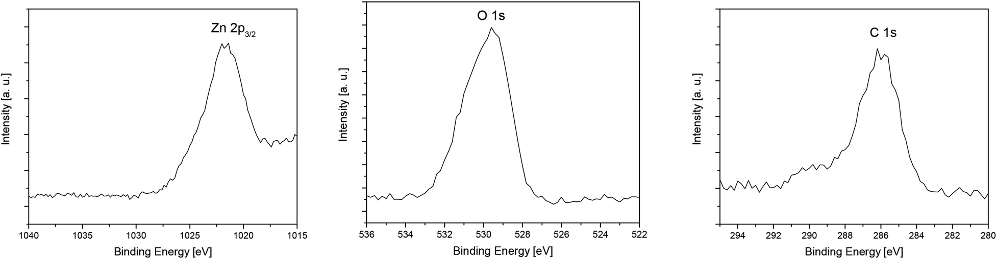 | ||
| Fig. 8 Ex situ detailed XPS spectra of Zn 2p3/2 (left), O 1s (middle) and C 1s (right) of layer C obtained from 7 by CVD. | ||
The XPS measurements of the layers confirm the presence of zinc, oxygen and carbon in the deposited films. The spectra of layers A–D show two main peaks located at 1044.2 eV and 1021.2 eV, which correlate with Zn 2p1/2 and Zn 2p3/2,60,61 respectively (Fig. 7, S11–S14 (see the ESI‡)). For all received films the binding energy difference between Zn 2p1/2 and Zn 2p3/2 is 23 eV, which is in good agreement for ZnO layers of different morphologies.61,62 This value together with the binding energy of Zn 2p1/2 and Zn 2p3/2 confirms the +2 oxidation state of Zn in the ZnO layers.61,62 Also, the position of O 1s at 529.6 eV verifies the formation of ZnO.61,62 Table 4 shows the composition of layers A–D after 5 min Ar ion sputtering, whereas the configuration of the surface is summarized in Table S1 (see the ESI‡).
| Layer | Layer composition [mol%] | ||
|---|---|---|---|
| Zn | O | C | |
| A | 36.3 | 46.4 | 17.3 |
| B | 42.2 | 34.1 | 23.7 |
| C | 49.2 | 38.5 | 12.3 |
| D | 44.4 | 33.8 | 21.8 |
The gas flow of the reactive gas influences the amount of the carbon in the layers. The higher the gas flow of the reactive gas, the lower the carbon contamination is, as illustrated for layers B and C (Tables 3 and 4). Also, the deposition temperature has an effect on the layer element composition. It was found that higher substrate temperatures result in an increase of carbon as demonstrated for D in comparison to C. Similar results were reported for the ZnO layers deposited by using diethyl zinc in the MOCVD process.63 In this context it is understandable that the carbon content of layer A is placed between the ones of films C and D, which is attributed to the lowest applied substrate temperature for deposit A using identical gas flow conditions as characteristic for layer B formation (Table 4).
The reason for the carbon contamination most likely is based on an uncontrolled and incomplete decomposition of the precursor depending on the used deposition conditions. Hence, the carbon impurity is higher on the surface areas then in the respective layers A–D (Tables 4 and S1 (ESI‡)), which can be ascribed to adsorbed precursor molecules 7 and/or hydrocarbons on the layer surface.
GIXRD measurements were carried out to prove the crystallinity of the as-deposited films. Representative, the diffractogram of layer D is depicted in Fig. 9, whereas the XRD patterns of A–C are presented in Fig. S22–S24 (see the ESI‡). It was found that the crystalline part of layers A–D consist of hexagonal ZnO (31.76°, 34.44°, 36.25°, 47.55°, 56.57°, 62.88°, 66.35°, 67.94°, 69.06°; [ICDD 01-070-8070]).
 | ||
| Fig. 9 GIXRD spectra of layer D with reflections of ZnO (red), applied deposition parameters are given in Table 3. | ||
Also, from Fig. 9 and S22–S24 (see the ESI‡) it can be seen that layers B–D show relatively sharp reflections, whereas the ones of layer A are less intense and broad. This cannot be ascribed to the different film thicknesses, since layers A and B demonstrate approximately the same thickness (Table 3). Presumably, in the case of layer A the lower deposition temperature of 320 °C affords smaller crystallite sizes or a lower fraction of crystalline material compared to layer B, which was deposited at 400 °C. The relatively large reflection at ca. 54° of A can be assigned to the Si/SiO2 substrate (Fig. S22, see the ESI‡).
Spin-coating
The spin-coating process allows the deposition of, for example, metal oxides by applying both volatile and non-volatile precursors.64,65 Hence, complexes 5 and 7 were utilized in MO layer formation (M = Mg, Zn) exploiting this technique. As substrate, silicon wafers with a native oxide layer were used (Experimental). The respective precursor solutions (0.5 M) were prepared by dissolving 5 in 2-methoxyethanol and 7 in ethanol (Experimental). The spin-coater was operated at 3000 rpm for 3 min (5) or 2 min (7). The appropriate deposition parameters are summarized in Table 5. The as-obtained layers were then heated to 250 °C and hold there for 10 min. Afterwards, they were heated-up in a horizontal tube furnace to 500 °C (MgO, layer E) or 450 °C (ZnO, layer F) with a heating rate of 10 °C min−1 and a holding time of 1 h under a flow of air (Table 5).Layer characterization
The morphology and the chemical composition of layers E and F were studied by SEM, EDX, XPS and GIXRD.As it can be seen from the SEM images (Fig. 10), the respective deposits are dense. The MgO layer shows a grainy morphology as compared to the respective conformal ZnO coating. Cross-sectional SEM studies were carried out for all samples in order to determine layer thicknesses and growth rates, respectively (Fig. 10, Table 5). Layer thicknesses of 80 nm for MgO (layer E) and 65 nm for ZnO (layer F) were observed.
 | ||
| Fig. 10 SEM Images of the respective MgO (layer E) and ZnO (layer F) (top view, left) and cross-sectional images (right) deposited on Si substrates covered with a native SiO2 layer. | ||
The elemental composition of the as-deposited films was investigated by EDX, showing the typical zinc and magnesium pattern (Fig. S9 and S10, see the ESI‡). In addition, signals for Si and C were detected of which the Si signal most likely originates from the Si/SiO2 substrate. The carbon impurities may stem from airborne hydrocarbon.
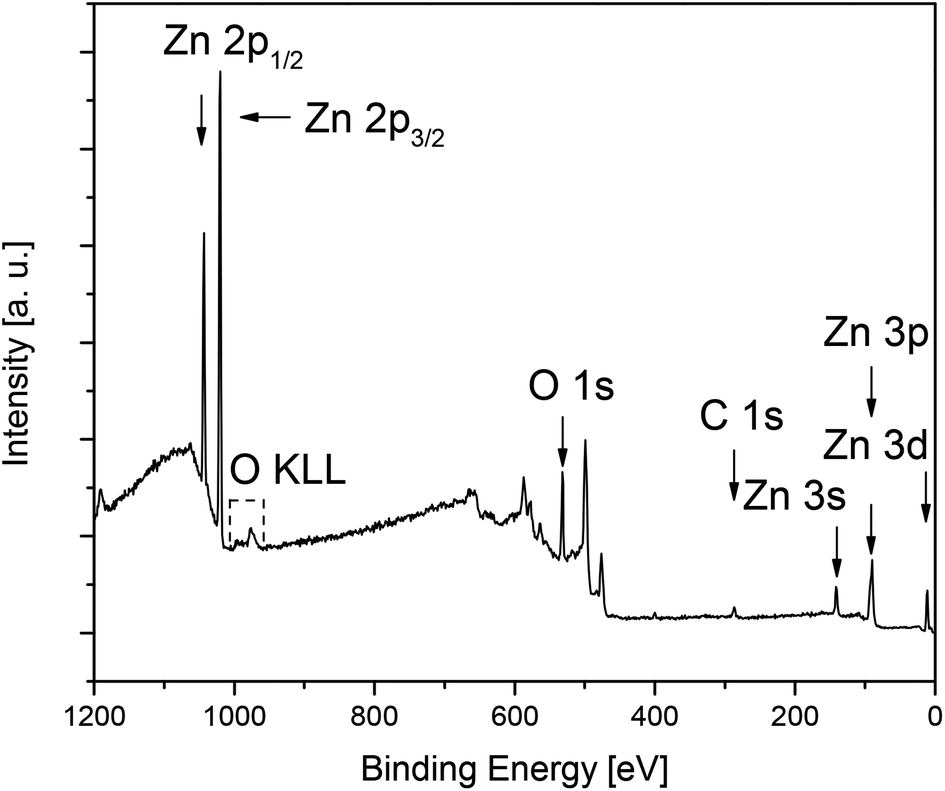
Additionally, XPS measurements for the spin-coated layers were performed to determine the elemental composition of the surface and the layer (Tables 6 and S1 (ESI‡)). Argon sputtering was performed to remove the topmost layer. The survey spectra of layers E and F are depicted in Fig. 11, whereas the spectra of the corresponding surface areas are summarized in Fig. S15 and S16 (see the ESI‡).
 | ||
| Fig. 11 Ex situ XPS survey spectra of layer E (left, obtained from 5) and layer F (right, obtained from 7) by spin-coating (Table 5) (after 5 min sputtering, Ar+, 4keV). | ||
Detailed XPS spectra of the respective deposits are depicted in Fig. S20 and S21 (see the ESI‡). The Mg 2p, Zn 2p3/2, Zn 3d, O 1s and C 1s peaks were used to calculate the chemical composition of the deposits. In case of layers E and F the elemental composition of the surfaces and layers is quite similar (Table S1,‡ Table 6). In general, the layers themselves consists of 37 mol% Mg (layer E), 38 mol% Zn (layer F), 53 mol% O, and ca. 9 mol% impurities (ZnO: carbon; MgO: carbon and fluorine) (Table 6). As fluorine source the decomposed Teflon grease could be identified, which was used in the synthesis of 5 and 7 and in the preparation of the spin-coating solutions. The peak positions of Mg 2p (50.8 eV), Zn 2p3/2 (1021.4 eV), Zn 2p1/2 (1044.4 eV), O 1s (530.5 eV, MgO; 529.6 eV, ZnO) are in agreement with earlier reports on these elements, confirming the formation of metal oxide films.49,61,62,66,67 In the case of MgO this could also be confirmed by the XPS detailed spectra of the C 1s peak, where also the KLL auger line of Mg at 307.9 eV was detected (Fig. 12).68
 | ||
| Fig. 12 Ex situ detailed XPS spectra of the C 1s peak of layer E. | ||
The difference of surface and layer composition for elements Zn/Mg and C could be assigned to the impurities of the topmost layer.
To evaluate the crystallinity of the as-deposited films, GIXRD measurements were performed (Experimental). The respective diffractograms of layers E and F are depicted in Fig. 13.
 | ||
| Fig. 13 GIXRD spectra of layer E (left) with reflections of MgO (red) and F (right) with reflections of ZnO (red), applied deposition parameters are given in Table 5. | ||
According to Fig. 13 the crystalline part of layer E consists of cubic MgO [ICDD 00-045-0946] as evidenced by the reflections at 36.86°, 42.83°, 62.17°, 74.52° and 78.45° representing the respective (111), (200), (220), (311) and (222) planes of the crystal structure. The other peaks match the reflections characteristic for silicon. In the case of layer F GIXRD measurements confirmed the formation of hexagonal ZnO in analogy to the results obtained by the CVD experiments. The exceptional sharp peak at around 47° consist of a reflection of hexagonal ZnO (47.55°; ICDD 01-070-8070) as well as a reflection (47.30°) originating from the Si substrate.
Conclusion
The synthesis of the magnesium and zinc diolates [M(OCHMeCH2NMeCH2)2] (5, M = Mg; 7, M = Zn) by treatment of diol (HOCHMeCH2NMeCH2)2 (3) with MR2 (4, M = Mg, R = Bu; 6, M = Zn, R = Et) is described. The investigation of the thermal behavior of 5 and 7 by TG indicated that decomposition of these complexes takes place between 100–480 °C under an atmosphere of argon, while under oxygen they decompose between 80–530 °C. The obtained residual masses 18.2% (5, O2) or 17.4% (5, Ar) and 30.1% (7, O2) are close to the theoretical residual mass of MgO (17.8%) and ZnO (30.4%). Contrastingly, under inert conditions a residual mass of 7 amounts to 22.1%, which is significantly lower than under oxygen, attributing to a partial evaporation of 7 during the heating process. TG-MS investigation of 7 confirmed that initially a decomposition between 120–230 °C occurs with a simultaneous partial evaporation of 7, whereas the 2nd step is characterized by the cleavage of Zn–O, N–C and C–C bonds. The vapor pressure of 7 was determined to 10.4 mbar at 160 °C, which is comparable with the one of [Zn{CF3C(O)CHC(O)CH3}2] (11.1 mbar at 140 °C),57 but significantly higher than for [Zn{CF3C(O)CHC(N(CH2)2OMe)Me}2] (0.53 mbar at 160 °C).58 Hence, 7 was used as CVD precursor for the deposition of ZnO. Deposition parameters have been varied to investigate their influence on the morphology of the metal oxide thin films. The growth of the ZnO films was investigated between 320 °C and 450 °C by variation of the gas flow of oxygen from 20 mL min−1 to 60 mL min−1. The highest growth rate of 3.1 nm min−1 was obtained at 450 °C, which is similar to the one (3.2 nm min−1) received for [Zn{MeC(O)CHC(N(CH2)3Me)Me}2],69 but significantly higher than for [Zn{MeC(O)CHC(N(CH2)2OMe)Me}2]70 (0.4 nm min−1). All obtained layers are close and coherent as proven by SEM analysis. The layer composition with the lowest carbon incorporations (12.3 mol%, XPS) was received by applying a substrate temperature of 400 °C and oxygen as co-reactant (flow rate of 60 mL min−1). However at advanced temperatures it was found that the respective layers contain a higher amount of carbon impurities. Contrastingly, the zinc β-ketoiminate [Zn{MeC(O)CHC(N(nBu))Me}2] produced ZnO films at 400 °C with a high content of carbon (23.7 mol%), while at 450 °C the C impurity is 9.9 mol% using nitrogen as carrier gas.69 Lower carbon contents (8.7 mol%) are found, when [Zn{EtOC(O)CHC(N(iPr))Me}2] is applied as CVD precursor, which is most likely due to the presence of the ethoxy moiety, serving as an intrinsic oxidant during the CVD process.40 However, layers without any C impurities are formed, when the zinc β-ketoiminates [Zn{MeC(O)CHC(N(CH2)nOMe)Me}2] (n = 2 or 3) were used for ZnO layer deposition under an atmosphere of oxygen.70 Furthermore, it was shown that higher substrate temperatures along with higher co-reactant gas flows result in more granulated surface morphologies. Complexes 5 and 7 were successfully used as spin-coating precursors for the deposition of MO thin films (M = Mg, Zn) on Si/SiO2 substrates. The as-obtained layers are dense and crack-free as well as smooth for the ZnO or grainy for the MgO deposits. All layers were investigated by EDX and XPS. Remarkable, the ZnO deposits obtained by spin-coating exhibit less carbon impurities (5.2 mol%) as the ones generated by CVD. Comparison of the surface and film composition reveals that the layers received by spin-coating are more resistant against ambient conditions than those ones obtained by CVD.Conflicts of interest
The authors declare no competing financial interests.Acknowledgements
We are grateful to the Federal Cluster of Excellence EXC 1075 MERGE (Technologies for Multifunctional Lightweight Structures) for financing this work. In addition, we thank Janine Freytag and Ute Stöβ for carrying out the elemental analyses, Dirk Rittrich and Cornelia Kowol for performing the SEM/EDX measurements and Natalia Rüffer for TGA measurements. The publication costs of this article were funded by the German Research Foundation/DFG-392676956 and the Technische Universität Chemnitz in the funding programme Open Access Publishing.References
- Y. Sun, J. H. Seo, C. J. Takacs, J. Seifter and A. J. Heeger, Adv. Mater., 2011, 23, 1679–1683 CrossRef CAS PubMed
.
- J. A. Alvarado, J. Luo, H. Juarez, M. Pacio, A. Cortes–Santiago, L. Liang, Z. G. Neale and G. Cao, Phys. Status Solidi A, 2018, 1800356 CrossRef
- E. M. C. Fortunato, P. M. C. Barquinha, A. C. M. B. G. Pimentel, A. M. F. Gonçalves, A. J. S. Marques, L. M. N. Pereira and R. F. P. Martins, Adv. Mater., 2005, 17, 590–594 CrossRef CAS
- T. Rembert, C. Battaglia, A. Anders and A. Javey, Adv. Mater., 2015, 27, 6090–6095 CrossRef CAS PubMed
- V. K. Kaushik, C. Mukherjee and P. K. Sen, J. Mater. Sci.: Mater. Electron., 2018, 29, 15156–15162 CrossRef CAS
- E. S. Nour, O. Nur and M. Willander, Semicond. Sci. Technol., 2017, 32, 1–11 CrossRef
- D. C. Agarwal, R. S. Chauhan, A. Kumar, D. Kabiraj, F. Singh, S. A. Khan, D. K. Avasthi, J. C. Pivin, M. Kumar, J. Ghatak and P. V. Satyam, J. Appl. Phys., 2006, 99, 123105 CrossRef
- B. Cho, H. Kim, D. Yang, N. K. Shrestha and M. M. Sung, RSC Adv., 2016, 6, 69027–69032 RSC
- M. A. Chougule, S. Sen and V. B. Patil, Ceram. Int., 2012, 38, 2685–2692 CrossRef CAS
- S. Pizzini, N. Butta, D. Narducci and M. Palladino, J. Electrochem. Soc., 1989, 136, 1945–1948 CrossRef CAS
- Z. L. Wang, Appl. Phys. A, 2007, 88, 7–15 CrossRef CAS
- L. Wang, Y. Yang, J. Ni, C. L. Stern and T. J. Marks, Chem. Mater., 2005, 17, 5697–5704 CrossRef CAS
- S. Vangelista, R. Mantovan, A. Lamperti, G. Tallarida, B. Kutrzeba-Kotowska, S. Spiga and M. Fanciulli, J. Phys. D: Appl. Phys., 2013, 46, 485304 CrossRef
- W.-Y. Chen, J.-S. Jeng and J.-S. Chen, ECS Solid State Lett., 2012, 1, N17–N19 CrossRef CAS
- G. Jiang, A. Liu, G. Liu, C. Zhu, Y. Meng, B. Shin, E. Fortunato, R. Martins and F. Shan, Appl. Phys. Lett., 2016, 109, 183508 CrossRef
- L. Yan, C. M. Lopez, R. P. Shrestha, E. A. Irene, A. A. Suvorova and M. Saunders, Appl. Phys. Lett., 2006, 88, 142901 CrossRef
- T. Urade, T. Iemori, M. Osawa, N. Nakayama and I. Morita, IEEE Trans. Electron Devices, 1976, 23, 313–318 Search PubMed
- X. Fu, Z. Song, G. Wu, J. Huang, X. Duo and C. Lin, J. Sol-Gel Sci. Technol., 1999, 16, 277–281 CrossRef CAS
- M. Copuroglu, L. H. K. Koh, S. O`Brien and G. M. Crean, J. Sol-Gel Sci. Technol., 2009, 52, 432–438 CrossRef CAS
- B. J. Lokhande and M. D. Uplane, Appl. Surf. Sci., 2000, 167, 243–246 CrossRef CAS
- S. Kurtaran, I. Akyuz and F. Atay, Appl. Surf. Sci., 2013, 265, 709–713 CrossRef CAS
- Y. Li, L. M. Wong, H. Xie, S. Wang and P.-C. Su, Surf. Coat. Technol., 2017, 320, 339–343 CrossRef CAS
- P. Ghosh and A. K. Sharma, Appl. Phys. A, 2016, 122, 357 CrossRef
- B. Ullah, V. Avrutin, S. Q. Li, S. Das, M. Monavarian, M. Toporkov, Ü. Özgür, P. Ruterana and H. Morkoç, Phys. Status Solidi RRL, 2016, 10, 682–686 CrossRef
- G. Carta, N. E. Habra, L. Crociani, G. Rossetto, P. Zanella, A. Zanella, G. Paolucci, D. Barreca and E. Tondello, Chem. Vap. Deposition, 2007, 13, 185–189 CrossRef CAS
- J.-H. Boo, S.-B. Lee, K.-S. Yu, W. Koh and Y. Kim, Thin Solid Films, 1999, 341, 63–67 CrossRef CAS
- D. Bekermann, D. Rogalla, H.-W. Becker, M. Winter, R. A. Fischer and A. Devi, Eur. J. Inorg. Chem., 2010, 1366–1372 CrossRef CAS
- B. B. Burton, D. N. Goldstein and S. M. George, J. Phys. Chem. C, 2009, 113, 1939–1946 CrossRef CAS
- E. Janocha and C. Pettenkofer, Appl. Surf. Sci., 2011, 257, 10031–10035 CrossRef CAS
- J. Reedijk and K. Poeppelmeier, 4.10-Metals-Gas-Phase Deposition and Applications, Comprehensive Inorganic Chemistry II, ed. H. Lang and S. Dietrich, Elsevier, Amsterdam, 2nd edn, 2013, pp. 211–269 Search PubMed
- J. Zabicky, Deposition of metals and metal oxides by means of metal enolates, The Chemistry of Metal Enolates, ed. H. Lang and R. Buschbeck, Wiley, Chichester, 2009, pp. 929–1017 Search PubMed
- J. A. Manzi, C. E. Knapp, I. P. Parkin and C. J. Carmalt, Eur. J. Inorg. Chem., 2015, 3658–3665 CrossRef CAS
- A. Chandramohan, N. V. Sibirev, V. G. Dubrovskii, M. C. Petty, A. J. Gallant and D. A. Zeze, Sci. Rep., 2017, 7, 40888 CrossRef PubMed
- W. Kern and R. C. Heim, J. Electrochem. Soc., 1970, 117, 562–568 CrossRef CAS
- A. P. Roth and D. F. Williams, J. Appl. Phys., 1981, 52, 6685–6692 CrossRef CAS
- S. K. Ghandhi, R. J. Field and J. R. Shealy, Appl. Phys. Lett., 1980, 37, 449–451 CrossRef CAS
- T. Maruyama and J. Shionoya, J. Mater. Sci. Lett., 1992, 11, 170–172 CrossRef CAS
- S. Jain, T. T. Kodas and M. Hampden-Smith, Chem. Vap. Deposition, 1998, 4, 51–59 CrossRef CAS
- J. Auld, D. J. Houlton, A. C. Jones, S. A. Rushworth, M. A. Malik, P. O`Brien and G. W. Critchlow, J. Mater. Chem., 1994, 4, 1249–1253 RSC
- J. S. Matthews, O. O. Onakoya, T. S. Ouattara and R. J. Butcher, Dalton Trans., 2006, 3806–3811 RSC
- H. Sato, T. Minami, T. Miyata, S. Takata and M. Ishii, Thin Solid Films, 1994, 246, 65–70 CrossRef CAS
- J.-J. Wu and S.-C. Liu, J. Phys. Chem. B, 2002, 106, 9546–9551 CrossRef CAS
- K. Black, A. C. Jones, P. R. Chalker, J. M. Gaskell, R. T. Murray, T. B. Joyce and S. A. Rushworth, J. Cryst. Growth, 2008, 310, 1010–1014 CrossRef CAS
- J. Musolf, E. Boeke, E. Waffenschmidt, X. He, M. Heuken and K. Heime, J. Alloys Compd., 1993, 195, 295–298 CrossRef CAS
- S. S. Lee, S. Y. Lee, J. S. Hyun, C. G. Kim and Y. Kim, Chem. Vap. Deposition, 2002, 8, 257–259 CrossRef CAS
- M. M. Sung, C. Kim, C. G. Kim and Y. Kim, J. Cryst. Growth, 2000, 210, 651–654 CrossRef CAS
- T. Maruyama and J. Shionoya, Jpn. J. Appl. Phys., 1990, 29, L 810–L 811 CrossRef CAS
- M. Vallet-Regi, M. Labeau, E. Garcia, M. V. Cabanas, J. M. Gonzalez-Calbet and G. Delabouglise, Physica C, 1991, 180, 57–60 CrossRef CAS
- E. Pousaneh, T. Rüffer, K. Assim, V. Dzhagan, J. Noll, D. R. T. Zahn, L. Mertens, M. Mehring, S. E. Schulz and H. Lang, RSC Adv., 2018, 8, 19668–19678 RSC
- E. S. Vikulova, K. V. Zherikova, I. V. Korolkov, L. N. Zelenina, T. P. Chusova, S. V. Sysoev, N. I. Alferova, N. B. Morozova and I. K. Igumenov, J. Therm. Anal. Calorim., 2014, 118, 849–856 CrossRef CAS
- J. R. Babcock, D. D. Benson, A. Wang, N. L. Edleman, J. A. Belot, M. V. Metz and T. J. Marks, Chem. Vap. Deposition, 2000, 6, 180–183 CrossRef CAS
- M. Smirnov, C. Baban and G. I. Rusu, Appl. Surf. Sci., 2010, 256, 2405–2408 CrossRef CAS
- J. Lee, T. Jeong, S. Yu, S. Jin, J. Heo, W. Yi and J. M. Kim, J. Vac. Sci. Technol., B: Microelectron. Nanometer Struct.--Process., Meas., Phenom., 2001, 19, 1366–1369 CrossRef CAS
- A. K. Balta, Ö. Ertek, N. Eker and I. Okur, Mater. Sci. Appl., 2015, 6, 40–47 CAS
- A. Nalbant, Ö. Ertek and I. Okur, Mater. Sci. Eng., B, 2013, 178, 368–374 CrossRef CAS
- A. Tuchscherer, C. Georgi, N. Roth, D. Schaarschmidt, T. Rüffer, T. Waechtler, S. E. Schulz, S. Oswald, T. Gessner and H. Lang, Eur. J. Inorg. Chem., 2012, 4867–4876 CrossRef CAS
- N. Matsubara and T. Kuwamoto, Inorg. Chem., 1985, 24, 2697–2701 CrossRef CAS
- S. D. Cosham, G. Kociok-Köhn, A. L. Johnson, J. A. Hamilton, M. S. Hill, K. C. Molloy and R. Castaing, Eur. J. Inorg. Chem., 2015, 4362–4372 CrossRef CAS
- J. H. Scofield, J. Electron Spectrosc. Relat. Phenom., 1976, 8, 129–137 CrossRef CAS
- NIST, X-Ray Photoelectron Spectroscopy Database, Version 4.1, National Institut Of Standards Technology, Gaithersburg, USA, 2012 Search PubMed
- R. Al-Gaashani, S. Radiman, A. R. Daud, N. Tabet and Y. Al-Douri, Ceram. Int., 2013, 39, 2283–2292 CrossRef CAS
- J. H. Zheng, Q. Jiang and J. S. Lian, Appl. Surf. Sci., 2011, 257, 5083–5087 CrossRef CAS
- J. G. Liu, S. L. Gu, S. M. Zhu, K. Tang, X.
D. Liu, H. Chen and Y. D. Zheng, J. Cryst. Growth, 2010, 312, 2710–2717 CrossRef CAS
- W. H. Jeong, J. H. Bae and H. J. Kim, IEEE Electron Device Lett., 2012, 33, 68–70 CAS
- E. Pousaneh, A. Preuß, K. Assim, J. Noll, A. Jakob, T. Rüffer and H. Lang, J. Rare Earths, 2017, 35, 1248–1254 CrossRef CAS
- J. S. Corneille, J.-W. He and D. W. Goodman, Surf. Sci., 1994, 306, 269–278 CrossRef CAS
- S. Ardizzone, C. L. Bianchi, M. Fadoni and B. Vercelli, Appl. Surf. Sci., 1997, 119, 253–259 CrossRef CAS
- J. F. Moulder, W. F. Stickle, P. E. Sobol and K. D. Bomben, Handbook of X-ray Photoelectron Spectroscopy: A Reference Book of Standard Spectra for Identification and Interpretation of XPS Data, Perkin-Elmer Corporation, Physical Electronics Division, Minnesota, 1992 Search PubMed
- J. Holmes, K. Johnson, B. Zhang, H. E. Katz and J. S. Matthews, Appl. Organomet. Chem., 2012, 26, 267–272 CrossRef CAS
- D. Bekermann, A. Ludwig, T. Toader, C. Maccato, D. Barreca, A. Gasparotto, C. Bock, A. D. Wieck, U. Kunze, E. Tondello, R. A. Fischer and A. Devi, Chem. Vap. Deposition, 2011, 17, 155–161 CrossRef CAS
Footnotes |
| † Dedicated to Prof. Dr Thomas F. Fässler on the occasion of his 60th birthday. |
| ‡ Electronic supplementary information (ESI) available: Fig. S1–S24, Table S1, NMR and IR spectra giving additional experimental data and spectroscopic details for all new compounds. See DOI: 10.1039/c9ra00585d |
| § NMR data are given for two diastereomers. |
| This journal is © The Royal Society of Chemistry 2019 |