
 Open Access Article
 This Open Access Article is licensed under a Creative Commons Attribution-Non Commercial 3.0 Unported Licence
Polymer/glass hybrid DC-MZI thermal optical switch for 3D-integrated chips
Yue Cao,
Yun-Ji Yi ,
Bai-Zhu Lin,
Yue Sun,
Xin-Chi Che,
Jie Zheng,
Fei Wang and
Da-Ming Zhang*
,
Bai-Zhu Lin,
Yue Sun,
Xin-Chi Che,
Jie Zheng,
Fei Wang and
Da-Ming Zhang*
State Key Laboratory of Integrated Optoelectronics, College of Electronic Science & Engineering, Jilin University, Changchun 130012, PR China. E-mail: zhangdm@jlu.edu.cn
First published on 5th April 2019
Abstract
A directional coupler (DC) Mach–Zehnder interferometer (MZI) thermal optical switch based on a polymer and glass waveguide hybrid for three-dimensional (3D)-integrated chips is demonstrated. The proposed thermal optical switch consists of a polymer waveguide and glass waveguide prepared using an ion-exchange technique. The two waveguide cores can achieve coupling in the vertical direction, improving the integration level on 3D-integrated chips, realizing the complementary advantages of polymer and glass materials. Because of the opposite thermal optical coefficients of polymer and glass materials, and the good stability, low transmission loss and large thermal conductivity of glass material, the device with a low power consumption, small dimensions, fast response time and high extinction ratio can be easily obtained. The optical field coupling between the graded refractive index and step refractive index in 3D directions was simulated. The optimized coupling efficiency is 99.82% with an open-window dimension (w) of 3 μm. The refractive index difference between the diffusion surface center and cladding (Δn) is 0.022. The properties of the DC-MZI thermal optical switch were optimized, achieving a switch power consumption of 5.16 mW, a rising time of 128.8 μs, a falling time of 249.5 μs without an air trench structure, and a switch power consumption of 3.74 mW, a rising time of 140.7 μs, a falling time of 256.3 μs after the etching of an air trench structure with a heating electrode width of 8 μm.
Introduction
Photonic integrated circuit (PIC) chips are key components of optoelectronic devices. PIC chips arouse a lot of attention because of their advances in terms of their low cost, optical connection point and power consumption, good reliability and capability to integrate different functional devices. However, the development of planar PICs is limited by the use of a single material system on the same substrate.1–3The use of three-dimensional (3D) hybrid integrated devices can solve the limitation of a one material system in PIC chips, which have the advantages of the integration of different materials on two-dimensional (2D) chips, 3D chips, micron waveguides nano waveguides and so on,4–9 thus, improving the chips' integration and performance. In recent years, optical chip interconnection has been widely used in new generation computers, optical communication, sensing, radar, satellite and other high-tech fields. Thus, related research on optical chips interconnected with 3D hybrid integrated chips has been studied more and has many advantages compared with 2D integrated chips. These advantages are: firstly, removing the chip dimension limitation on the plane, multiplying the connection points of integration, optics and electrics; secondly, making use of the multilayer structure and material advantages, maximally improving the chip performance and function; thirdly, integration with microfluidics to realize a lab-on-a-chip;10 fourthly, integration with microelectronic chips to form optoelectronic integrated chips (OEIC).
3D hybrid integration is divided into a hybrid waveguide structure with a one layer structure and in a multilayer structure. For the one layer structure, the different individual devices are usually connected using simple methods such as simple splicing of individual device units and end face attachment. For the multilayer structure, in order to overcome the plane limitation on the chip, different coupling methods of 3D integrated devices have been proposed, including multilayer silica nitride platform coupling,11 direct laser writing coupling,12 easy connection of interface,13 a bonding technique between active and passive glass.14 The multilayer structure is more suitable for the hybrid integration of various kinds of materials. Therefore, optical manipulation and switching between different layers are the essential issues.
To realize optical manipulation and switching in the multilayer structure, the coupling structure can be applied to a multilayer waveguide, including an adhesive bonding structure15 and parallel coupling structure.16 These structures do not possess tuning functions. Therefore, the change in the optical path in the waveguide can be realized using a thermal tuning method. In 2003, Chan et al. proposed a wide-angle X-junction polymeric thermal optic switch with a driving power of 145 mW.17 In 2016, Yu et al. fabricated an X-junction optical attenuator based on a polymer/silica hybrid waveguide with a 21 mW electrical input power at 650 nm.18 For a polymer and glass hybrid waveguide structure, the switch power consumption and switch time are lower because of the opposite thermo-optical coefficient of polymer and inorganic material. Furthermore, compared to the X-junction structure, the directional coupler Mach–Zehnder interferometer (DC-MZI) optical switch exhibits lower power consumption.19 However, during the fabrication process of multilayer devices, especially for the parallel waveguide coupling method, it is easy to cause unevenness of the film using a spin coating and silica growth process.
In this paper, a DC-MZI thermal optical switch composed of a polymer waveguide and glass waveguide is demonstrated. The polymer and glass hybrid structure is beneficial for reducing the power consumption and response time because of the opposite coefficients of polymer and glass materials. The glass waveguide is fabricated using an ion exchange technique, which can realize a flat surface film with a multilayer structure. Furthermore, the polymer material has good doping properties and compatibility with the glass substrate, which is beneficial for the refractive index and dimension matching with the glass waveguide. The glass material has good stability and low transmission loss, and can be used as a passive waveguide and pumping structure. Therefore, the polymer and glass hybrid structure can realize the complementary advantages of the two materials. In this study, the coupling between the step refractive index of the polymer waveguide and the graded refractive index of the glass waveguide has been simulated using COMSOL Multiphysics Modeling Software. Meanwhile, the device structure, dimension and refractive index was optimized for the 3D hybrid integration structure. The coupling parameters and switching properties were also analysed.
Design and simulation
The structure of the 3D hybrid DC-MZI thermal optic switch is shown in Fig. 1 (a = b = 4 μm; w = the open-window size of ion-exchanged waveguide, d = coupling gap, h = is the height of the metal heater over the polymer waveguide, m1 = the length of the metal heater, m2 = the weight of the metal heater, L0 = the coupling length of waveguide in vertical direction, and L′ = the uncoupling length of waveguide). This thermal optic switch consists of a polymer waveguide core, an ion-exchanged glass waveguide core, a metal electrode and the waveguide claddings. The waveguide plan-section and cross-section along segment 3 are shown in Fig. 1(b) and (c), respectively. The switch was designed so that half of the optical signal launched from port ‘a’ could be coupled to the bottom waveguide after the first coupling region. Almost all of the optical signal will be coupled to the bottom waveguide after the second coupling region in the vertical direction (cross state). When heating the electrode, the refractive index of the polymer waveguide could easily be changed because of the high thermo-optical coefficient of the polymer material, leading to the change of the optical path from the cross through state (light is output from b′) to the pass through state (light is output from a′) and realizing switching function.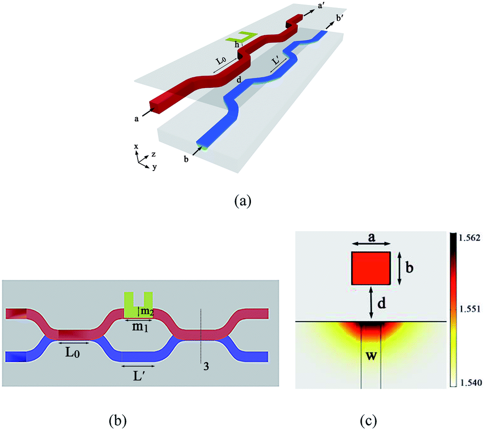 | ||
| Fig. 1 A schematic representation of the polymer-glass hybrid DC-MZI thermal optic switch (a) with 3D structure, (b) in the y–z plane, (c) in the x–y plane. (The polymer waveguide is represented in pink, whereas the glass waveguide is in blue.) | ||
The fabrication process of this thermal optic switch is as follows. Firstly, the glass core layer can be fabricated using an ion-exchange technique on a glass substrate. Secondly, the polymer material was spin-coated onto the glass core layer to form a middle cladding. Thirdly, the polymer core layer was formed by spin-coating polymer material onto the cured middle cladding and applying photolithography with a MZI waveguide mask. Fourthly, the polymer cladding material was coated onto the polymer core layer to form a polymer upper cladding. Fifthly, the aluminium (Al) film was deposited on polymer upper cladding using thermal evaporation. Then, the positive photoresist (BP-212) was spin-coated onto the Al film. Finally, the heating electrode was fabricated using conventional photolithography and wet etching processes.
Theoretical model and optical field
The glass waveguide can be fabricated using ion-exchange technology. The refractive index profile of the glass waveguide (n(x, y, z)) can be calculated using:14
 | (1) |
N(x, t) = N0![[thin space (1/6-em)]](https://www.rsc.org/images/entities/char_2009.gif) erfc(x/W0) erfc(x/W0)
| (2) |
 | (3) |
The coupling between the polymer waveguide and the glass waveguide was simulated. The coupling of the light field in two hybrid waveguides depended on the open-window dimension of the ion-exchanged waveguide, the concentration difference, and the diffusion time. The effective refractive index of the two waveguides could be equalized by adjusting the parameters of the refractive index change between the diffusion surface core and the diffusion time at the same width of open-window. The calculated results are given in Table 1. The relationships between the refractive index difference (Δn) and coupling efficiency with different open-window dimensions of the ion-exchanged waveguide are shown in Fig. 2(a). The curve of the refractive index difference and coupling gap are shown in Fig. 2(b). This indicates that the maximum coupling efficiency was obtained with a coupling gap of 4.5 μm.
| Δn | t (min) (w = 2 μm) | t (min) (w = 3 μm) | t (min) (w = 4 μm) |
|---|---|---|---|
| a The refractive index of the substrate = 1.54, the refractive index of the cladding = 1.54, the refractive index of the polymer core = 1.5523, D = 0.068 min−1. | |||
| 0.016 | 110.4 | 91.9 | 89.4 |
| 0.018 | 79.2 | 64.9 | 63 |
| 0.02 | 58.8 | 48.2 | 46.6 |
| 0.022 | 46.1 | 37.2 | 35.8 |
| 0.024 | 36.9 | 29.4 | 28.2 |
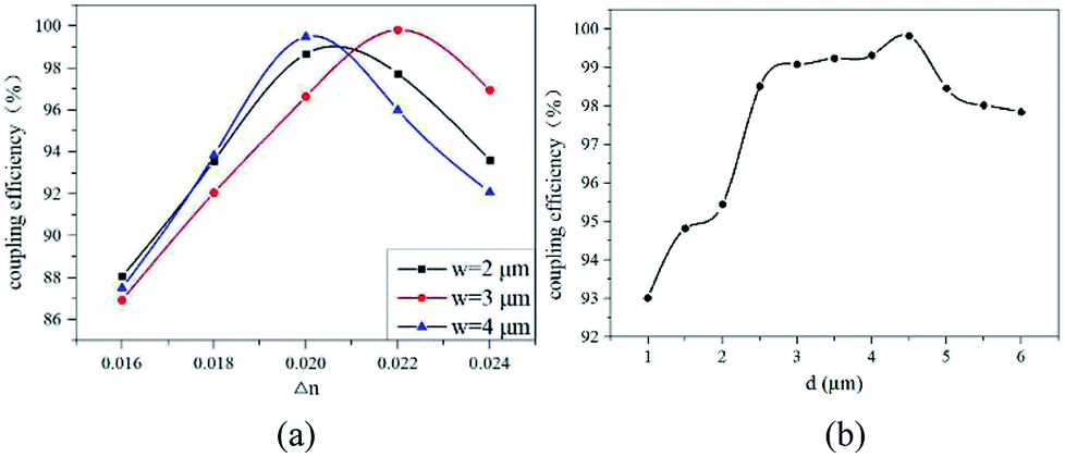 | ||
| Fig. 2 The curves of coupling efficiency with different (a) refractive index difference between the diffusion surface center and cladding, and (b) coupling gap with an open-window size of 3 μm. | ||
Because the coupling of the waveguides was related to the device dimension and refractive index, when the optical field dimension was mismatching, the complete coupling cannot be achieved even if the effective refractive indices of the two waveguides were equal. The 3D distribution of the light field in the x–y directions is shown in Fig. 3 with a Δn of 0.022 and 0.016, respectively (w = 3 μm). The parameters of Ez and E define the electric field of the boundary mode in the z direction and the electric field norm, respectively. The results of this show that the light field was more concentrated in the core of the two waveguides with a Δn of 0.022 compared with a Δn of 0.016. The distribution of the light field in the x–y–z, x–z and y–z directions is shown in Fig. 4 (w = 3 μm, Δn = 0.022). The half of the optical signal launched from the port ‘a’ could be coupled to the bottom waveguide after the first coupling region with a coupling length of the waveguide in the vertical direction of 4.5 mm. Almost all of the optical signal could be coupled to the bottom waveguide after the second coupling region in the vertical direction, which could realize 99.82% coupling.
 | ||
| Fig. 3 The 3D distribution of the light field for the hybrid DC-MZI thermal optic switch at the x–y direction: (a) the light field simulation with a w of 3 μm and Δn of 0.022, (b) the light field simulation with a w of 3 μm and Δn of 0.016. | ||
 | ||
| Fig. 4 The three-dimensional distribution of the light field for the hybrid DC-MZI thermal optic switch. (a) The light field simulation at the x–y–z direction, (b) the light field simulation at the y–z direction, and (c) the light field simulation at the x–z direction. | ||
Thermal field optimization
To design a hybrid DC-MZI thermal optic switch with low power consumption and superior response time, there were several factors including device structure and heating electrode position that were considered. Because of the large thermal optical coefficient of the polymer material, the effective refractive index of the thermal optical switch could be easily changed when heating the electrode. According to the formula: ΔΦ = (2Π/λ) × ΔN × m1 (ΔΦ = waveguide phase change, λ = waveguide wavelength, and ΔN = effective refractive index change), the phase of light in the polymer waveguide could be changed when the effective refractive index of the thermal optical switch changed. If the ΔΦ = Π/2, the optical path switching function could be realized, so that the light output was from the b′ port. The curves of the phase change and the effective refractive index with the device structure without air trench and etched air trench at both ends of the heating electrode are presented in Fig. 5.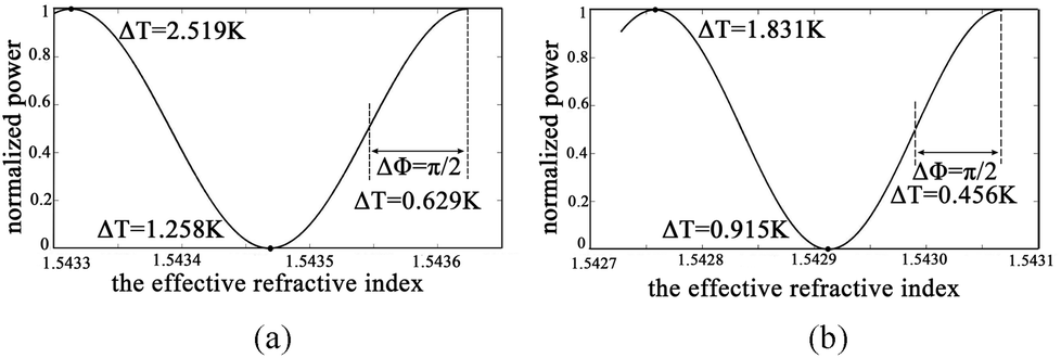 | ||
| Fig. 5 The curves of the phase change with different effective refractive index, (a) structure 1: DC-MZI thermal optical switch without etched air trench, and (b) structure 2: DC-MZI thermal optical switch with etched air trench at both ends of the heating electrode. | ||
The distributions of the thermal fields for structure 1 and structure 2, respectively, are shown in Fig. 6 (heating electrode width m2 = 8 μm and m1 = 0.5 cm, the thermal optical coefficient of polymer = −2.36 × 10⁻⁴, the thermal optical coefficient of glass = 1.28 × 10⁻⁵). Compared with the initial temperature at 293.15 °C, the electrode temperature increases 0.629 °C for structure 1 (switch power consumption = 5.16 mW) and 0.456 °C for structure 2 (switch power consumption = 3.74 mW).20
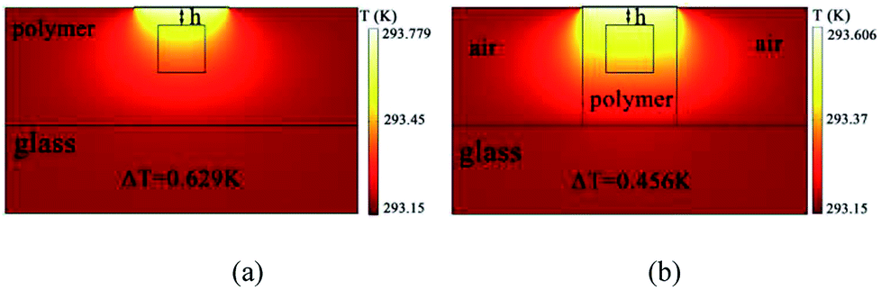 | ||
| Fig. 6 The distribution of thermal field for hybrid DC-MZI thermal optical switch. (a) Structure 1: DC-MZI thermal optical switch without etched air trench; (b) structure 2: DC-MZI thermal optical switch with etched air trench at both ends of the heating electrode. | ||
Another consideration for the heating electrode position is the requirement that the light absorption of the electrode should be decreased whereas the variable of waveguide refractive index should be increased. The relationship between the distance from the heating electrode to the top of polymer waveguide (h) and the light absorption of the electrode (α) is shown in Fig. 7. The black line represents the heating electrode absorption curve of structure 1, whereas the red line represents the heating electrode absorption curve of structure 2. This shows that the light absorption of the electrode is 0.279 dB cm−1 and 0.288 dB cm−1 with an h of 1.5 μm for structure 1 and structure 2, respectively.
 | ||
| Fig. 7 The relationship between the distance from the heating electrode to the top of the polymer waveguide and the light absorption of the electrode. | ||
The relationship between the distance from the heating electrode to the top of polymer waveguide (h) and the heater efficiency for the polymer waveguide core layer (η) is shown in Fig. 8. The formula of the heater efficiency for the polymer waveguide core layer is expressed as: η = (Tc − T0)/(Th − T0) (Th = electrode heating temperature, T0 = initial temperature of thermal optical switch, and Tc = the temperature of the center polymer waveguide core layer). This showed that the DC-MZI thermal optical switch with an etched air trench had a higher heating efficiency. The heater efficiency for the polymer waveguide core layer decreased as the distance from heating electrode to the top of the polymer waveguide increased. A heater efficiency of 53.51% was obtained for with the DC-MZI thermal optical switch with an etched air trench.
 | ||
| Fig. 8 The relationship between the distance from the heating electrode to the top of the polymer waveguide and the heater efficiency for the polymer waveguide core layer. | ||
Fig. 9 shows the simulated response time curves of the DC-MZI thermal optical switch (m2 = 8 μm, h = 2 μm). Firstly, according to the formula: ΔΦ = (2Π/λ) × ΔN × m1, when heating the electrode, the effective refractive index of the thermal optical switch will change. Then, the phase changes can be obtained. If ΔΦ = Π/2, the optical path switching function can be realized. Secondly, the transient thermal field in the center of the polymer waveguide core layer was analysed using COMSOL Multiphysics Modeling Software. Finally, the response time of the thermal optical switch can be obtained using the multi-physical field simulation model. As indicated in Fig. 8(a), Because of the large thermal conductivity of the glass material, the response time was affected by the distance between the polymer waveguide and the glass substrate (d) (the rising time and falling time were 128.8 μs and 249.5 μs, respectively). As shown in Fig. 8(b), the response time could be improved by using an etched air trench structure (the rising time and falling time were 140.7 μs and 256.3 μs, respectively).
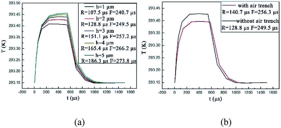 | ||
| Fig. 9 The response time curves of the DC-MZI thermo optical switch, (a) with different distances between the polymer waveguide and glass substrate, and (b) with different device structures. | ||
Conclusions
In summary, a DC-MZI thermal optical switch based on a polymer and glass waveguide hybrid for 3D integrated chips was designed. This thermal optical switch could realize a 99.82% coupling in the vertical direction with a w of 3 μm and a Δn of 0.022. Because of opposite thermal optical coefficients of the polymer and the glass material, and the good stability, there was a low transmission loss and a large thermal conductivity of the glass material. The switch power consumption is 5.16 mW and 3.74 mW for structure 1 and structure 2, respectively, with a phase change of Π/2, improving the heating efficiency and reducing the power consumption. The DC-MZI thermal optical switch was optimized to achieve a rising time of 128.8 μs, falling time of 249.5 μs for structure 1 and a rising time of 140.7 μs, falling time of 256.3 μs for structure 2 with a heating electrode width of 8 μm and an uncoupled length of 0.5 cm. This DC-MZI thermal optical switch can be applied to the field of optical interconnects,21 chemical sensing22 and lithium batteries.23Funding
This work was supported by the Science and Technology Development Plan of Jilin Province (20190302010GX), the National Key Research and Development Plan of China (Grant No. 2016YFB0402502), the National Natural Science Foundation of China (61605057, 61575076) and the Excellent Youth Foundation of Jilin Province (20170520158JH).Conflicts of interest
There are no conflicts to declare.References
- J. Gosciniak and S. I. Bozhevolnyi, Performance of thermo-optic components based on dielectric-loaded surface plasmon polariton waveguides, Sci. Rep., 2013, 3, 1803–1810 CrossRef.
- S. Papaioannou, D. Kalavrouziotis, K. Vyrsokinos, J. Weeber, K. Hassan, L. Markey, A. Dereux, A. Kumar, S. I. Bozhevolnyi, M. Baus, T. Tekin, D. Apostolopoulos, H. Avramopoulos and N. Pleros, Active plasmonics in WDM traffic switching applications, Sci. Rep., 2012, 2, 652–660 CrossRef PubMed.
- P. Berini and I. D. Leon, Surface plasmon–polariton amplifiers and lasers, Nat. Photonics, 2012, 6, 16–24 CrossRef CAS.
- W. Freude, 100 GHz silica–organic hybrid modulator Open, Light: Sci. Appl., 2014, 3, e176–176 Search PubMed.
- Y. Enami, A. K.-Y. Jen, G. Meredith and N. Peyghambarian, Hybrid electro-optic polymer/sol-gel waveguide modulators fabricated by all-wet etching process, using straight channel and mach-zehnder waveguides, Proc. SPIE-Int. Soc. Opt. Eng., 2004, 5350, 89–96 CrossRef CAS.
- D. Dai, Passive technologies for future large-scale photonic integrated circuits on silicon: Polarization handling, light non-reciprocity and loss reduction, Light: Sci. Appl., 2012, 1, e1–12 CrossRef.
- Y. Yang, A. Q. Liu, L. K. Chin, X. M. Zhang, D. P. Tsai, C. L. Lin, C. Lu, G. P. Wang and N. I. Zheludev, Optofluidic waveguide as a transformation optics device for lightwave bending and manipulation, Nat. Commun., 2012, 3, 651–657 CrossRef CAS PubMed.
- C. J. Brooks, A. P. Knights and P. E. Jessop, Vertically-integrated multimode interferometer coupler for 3D photonic circuits in SOI, Opt. Express, 2006, 14, 6628–6633 CrossRef.
- P. Shashank, G. Barun and N. Ajay, Terahertz plasmonic waveguides created via 3D printing, Opt. Express, 2013, 21, 24422–24430 CrossRef PubMed.
- M. V. Rebeca, O. Roberto, C. Marina, C. Marcella, D. Chaitanya, J. W. M. Hoekstra Hugo, P. Markus, van den V. Hans, R. Roberta and C. Giulio, Optical sensing in microfluidic lab-on-a-chip by femtosecond-laser-written waveguides, Anal. Bioanal. Chem., 2009, 393, 1209–1216 CrossRef PubMed.
- K. P. Shang, S. Pathak, B. B. Guan, G. Y. Liu and S. J. B. Yoo, Low-loss compact multilayer silica nitride platform for 3D photonic integrated circuits, Opt. Express, 2015, 23, 21334–21342 CrossRef CAS PubMed.
- M. Schumann, T. Buckmann, N. Gruhler, M. Wegener and W. Pernice, “Hybrid 2D–3D optical devices for integrated optics by direct laser writing open, Light: Sci. Appl., 2014, 3, e175–183 CrossRef CAS.
- B. B. Guan, R. P. Scott, C. Qin, N. K. Fontaine, T. H. Su, C. Ferrari, M. Cappuzzo, F. Klemens, B. Keller, M. Earnshaw and S. J. B. Yoo, Free-space coherent optical communication with orbital angular, momentum multiplexing/demultiplexing using a hybrid 3D photonic integrated circuit, Opt. Express, 2014, 22, 145–156 CrossRef PubMed.
- V. Donzella, V. Toccafondo, S. Faralli, F. Di Pasquale., C. Cassagnettes, D. Barbier and H. H. Figueroa, Ion-exchanged Er3+/Yb3+ co-doped waveguide amplifiers longitudinally pumped by broad area lasers, Opt. Express, 2010, 18, 12690–12701 CrossRef CAS PubMed.
- D. V. Tishinin, P. D. Dapkus, A. E. Bond, I. Kim, C. K. Lin and J. O'Brien., Vertical resonant couplers with precise coupling efficiency control fabricated by wafer bonding, IEEE Photonics Technol. Lett., 1999, 11, 1003–1005 Search PubMed.
- Y. Cao, B. Z. Lin, Y. Sun, Y. J. Yi, Y. J. Liu, J. Zheng, F. Wang and D. M. Zhang, Polymer-Silica Hybrid On-Chip Amplifier with Vertical Pumping Method, Sci. Rep., 2018, 8, 1–9 CrossRef PubMed.
- H. P. Chan, C. K. Chow and A. K. Das, A wide-angle X-junction polymeric thermooptic digital switch with low crosstalk, IEEE Photonics Technol. Lett., 2003, 15, 1210–1212 Search PubMed.
- Y.-Y. Yu, X.-Q. Sun, L.-T. Ji, G.-B. He, X.-B. Wang, Y.-J. Yi, C.-M. Chen, F. Wang and D.-M. Zhang, The 650-nm variable optical attenuator based on polymer/silica hybrid waveguide, Chin. Phys., 2016, 25, 164–171 Search PubMed.
- S. Yue, C. Yue, Yi. Yunji, T. Liang, Z. Yao, Z. Jie, W. Fei and Z. Daming, A low-power consumption MZI thermal optical switch with a graphene-assisted heating layer and air trench, RSC Adv., 2017, 7, 39922–39927 RSC.
- L. Yu-Fen, W. Fei, W. Xi-Bin, S. Xiao-Qiang, S. Jian, G. Hong-Jun, C. Chang-Ming and Z. Da-Ming, Thermal field analysis of polymer/silica hybrid waveguide thermo-optic switch, Opt. Commun., 2015, 356, 79–83 CrossRef.
- X. Zhang, A. Hosseini, X. Lin, H. Subbaraman and R. T. Chen, Polymer-based Hybrid Integrated Photonic Devices for Silicon On-chip Modulation and Board-level Optical Interconnects, IEEE J. Sel. Top. Quantum Electron., 2013, 19, 196–210 Search PubMed.
- T. Tita, M. Mangirdas, G. Roaldas, B. Yves and P. Domas, Hybrid laser 3D microprocessing in glass/polymer micromechanical sensor: towards chemical sensing applications, 3D Printed Optics and Additive Photonic Manufacturing, 2018, vol. 10675, p. 106750C Search PubMed.
- I. Villaluenga, K. H. Wujcik, W. Tong, D. Devaux, D. H. C. Wong and J. M. Desimone, Compliant glass–polymer hybrid single ion-conducting electrolytes for lithium batteries, Proc. Natl. Acad. Sci. U. S. A., 2016, 113, 52–57 CrossRef CAS PubMed.
| This journal is © The Royal Society of Chemistry 2019 |