
 Open Access Article
 This Open Access Article is licensed under a Creative Commons Attribution-Non Commercial 3.0 Unported Licence
Theoretical studies on the structures and properties of doped graphenes with and without an external electrical field†
Yuhua Wang *a,
Weihua Wangb,
Shuyun Zhub,
Ge Yang*c,
Zhiqiang Zhangd and
Ping Li*b
*a,
Weihua Wangb,
Shuyun Zhub,
Ge Yang*c,
Zhiqiang Zhangd and
Ping Li*b
aAdministrative Office of Laboratory and Equipment, Qufu Normal University, 273165, Qufu, Shandong, PR China. E-mail: hxlwe@126.com
bCollege of Chemistry and Chemical Engineering, Qufu Normal University, 273165, Qufu, Shandong, PR China. E-mail: lpsdu@sdu.edu.cn
cThe School of Life Sciences, Qufu Normal University, 273165, Qufu, Shandong, PR China. E-mail: yangge100@126.com
dDepartment of Material and Chemical Engineering, Zhengzhou University of Light Industry, Zhengzhou 450002, Henan, PR China
First published on 16th April 2019
Abstract
To expand the applications of graphene in optoelectronic devices, B, Al, Si, Ge, As, and Sb doped graphenes (marked as B-G, Al-G, Si-G, Ge-G, As-G, and Sb-G, respectively) were synthesised. The geometric structures, population analyses, and also electronic and optical properties of these doped graphene materials were investigated employing the density functional theory (DFT) method. It was shown that the band gaps of doped graphenes were opened and their absorption spectra were red-shifted by the addition of doping atoms, and their dielectric functions and refractive indexes of low frequency were decreased compared with those of pure graphene. Moreover, the electronic and optical properties of doped graphenes under an external electrical field ranging from −0.4 to 1.2 eV Å−1 have been explored. It was found that the band gaps of As-G and Sb-G were increased to 0.864 and 1.841 eV under a 1.2 eV Å−1 external electrical field, respectively. On the contrary, the band gaps of B-G, Al-G, Si-G, and Ge-G were decreased with the increase of the external electrical field intensity. Additionally, the absorption peaks of B-G, Al-G, Si-G, and Ge-G were red-shifted upon applying the external electrical field. Correspondingly, their dielectric functions and refractive indexes of low frequency were increased. Surprisingly, the absorption spectra, dielectric functions, and refractive indexes of As-G and Sb-G have no significant changes.
1. Introduction
Graphene is a carbon material with a two-dimensional network structure of atomic thickness. Many scholars have been interested in studying graphene since its successful preparation.1,2 Graphene demonstrates incredible electronic performance,3–5 outstanding optical properties,6 interesting thermal performance,7 larger specific surface area,8,9 excellent elastic modules etc.10 Especially, the incredible electronic performance makes graphene a potential candidate in electronic devices.11–13 However, the zero band gap of graphene needs to be opened to expand its range of applications in photonics, integrated circuits, solar cells etc. So far, many chemical and physical methods have been used to open the band gap of graphene. Most chemical methods were achieved mainly through hybridization, for example mono and double doped graphenes were experimentally fabricated and theoretically predicted to show a change in electronic properties. The single dopant graphenes mainly comprise a main group element or subgroup element. The main group elements include B,14 N,15 Al,16,17 P,17,18 S,17–21 Si,22–24 Se25,26 etc. The subgroup elements include Mg, Co, Ni,27 Fe,28–30 U, Th31 etc. Double doped graphenes include P–N,32,33 S–N,34,35 Si–N,35,36 Be–B,37 Be–N,38 Be–S,39 N–Al,40 N–B41,42 etc. Some physical methods were also applied to open the band gap of graphene. For example, two-dimensional graphenes were clipped into one-dimensional nanoribbons;43,44 a tensile or shear strain was applied on the graphene sheet;45,46 graphene nano-mesh was obtained by adding topological nano-holes into graphene sheet,47 an electric field was applied for the graphene-base system48 etc. On the other hand, the optical properties of doped graphenes were reported scarcely although the electronic properties were studied.21,30Some studies have shown that the electrical and optical properties of graphene are affected not only by the impurity atoms but also by the content of the impurity atoms. Shuai et al. reported that the band gap of Si doped graphene was increased with increasing Si concentration in graphene sheet. The refractive index and absorption spectra of the graphene were also changed after Si doping.24 Jindal et al. introduced that the electronic properties and absorption spectra of graphene were not affected after single B and N doping except that the absorption spectra of graphene occurred red-shift after B/N codoping at high contents.48 Nourbakhsh et al. reported higher refractive index of Fe doped graphene and Co doped graphene sheets.30 However, these studies are only limited to the studies on the electronic and optical properties of metal or non-metal doped graphenes. A very little amount of studies are done to explore the influences of metallic and metalloid-based dopants on the structural, electronic and optical properties of graphene under external electrical field.
In this study, the metallic and metalloid-based dopants (i.e. boron (B), silicon (Si), aluminum (Al), germanium (Ge), arsenic (As), stibonium (Sb)) doped graphenes (marked as B-G, Si-G, Al-G, Ge-G, As-G, and Sb-G, respectively) model are built to investigate the effect of various dopants on the electronic and optical properties of graphene sheet by employing DFT method. Meanwhile, the electronic and optical properties of doped graphenes under external electrical field ranging from −0.4 to 1.2 eV Å−1 have also been explored. Considering the fact that the content of dopant atoms is proportional to the properties of doped graphenes,24 four dopant atoms are introduced into graphene sheets, and the structures of doped graphenes are detailedly analyzed.
2. Models and methods
In this study, the structures, electronic and optical properties of the doped graphenes mentioned above are investigated employing the CASTEP module.21,40 According to the literature, the generalized gradient approximation (GGA) with Perdew–Burke–Ernzerhof (PBE) has been used for exchange–correlation functional to simulate the properties of the doped graphenes. Moreover, the Grimme method for DFT-D correction and the spin unrestriction are selected to calculate the van der Waals (vdW) interactions and the different orbital spins, respectively.21,30,40 Ultrasoft pseudo-potential is selected to perform the core treatment.4 × 4 × 1 supercell was built to model the original graphene (OG) sheet. For doped graphenes, four dopant atoms are introduced into graphene sheet. The vacuum space of 20 Å is set in the direction perpendicular to the sheet to avoid the interactions between periodic structures. The energy cutoff is set to 400 eV. A 17 × 17 × 1 and 36 × 36 × 1 mesh of k-point is used for geometry optimization and electronic structure calculations of OG and doped graphenes, respectively. All atoms are allowed to relax and convergence in energy, force, and displacement are 2 × 10⁻⁵ eV, 0.004 Ha Å−1, and 0.005 Å, respectively. Moreover, the set of 36 × 36 × 1 k-mesh and 50 empty bands were used for the calculation of optical properties.
3. Results and discussion
3.1 Structure analysis
In order to verify the reliability of the established model and data, the electronic and geometric structures of graphene are calculated and shown in Fig. 1. As shown in Fig. 1(a), the length of C–C bond of OG is 1.420 Å, which is consistent with the literature data.37,39 Fig. 1(b) shows the band gap and total density of states (DOS) of OG. Obviously, the band gap of OG is zero at Dirac point, which is consistent with the result of the experimental study and theoretical simulation.41 So, the reliability of the established model and simulation methods should be confirmed. Under the same simulation condition, the optimized doped graphenes are shown in Fig. 2. Because the covalent radii of B (85 pm), Al (126 pm), Si (116 pm), Ge (124 pm), As (121 pm), and Sb (140 pm) atoms are different from that of C (75 pm) atom, the different degrees of structural deformation for doped graphenes will occur. In view of the position of B, Al, and Si atoms in the periodic table and the purpose of obtaining the maximum band gap of graphene, B, Al, and Si atoms replace carbon atom of OG in situ. However, due to the large radii of As and Sb atoms, their positions in the doped graphenes are set outwards from the surface of graphene. For Ge atom, preliminary analysis indicates that the band gap of in situ replaced graphene was larger than that of protruded from the surface of graphene. As presented in Table 1, the calculated bond lengths of B–C (1.503 Å), Al–C (1.764 Å), Si–C (1.684 Å), and Ge–C (1.740 Å) are consistent with previous studies.24,30,37,40 As for the As–C and Sb–C bonds, they are 1.875 and 2.109 Å, respectively. Moreover, the C–C bonds around the dopant atoms are also changed by the introduction of these dopant atoms with large covalent radii. The ortho, meta, and para C atoms around the dopant atoms are marked as C1, C2, and C3, respectively. Analyses of the neighboring (C1–C2) and next-adjacent (C2–C3) C–C bonds around the dopant atoms for all the structures suggest that the bond lengths of C1–C2 (from 1.420 to 1.435 Å) are close to that of C–C (1.420 Å) of OG. While the bond lengths of C2–C3 (from 1.478 to 1.546 Å) are longer than that of C–C of OG. These phenomena may be attributed to the stronger interaction between the dopant atom and ortho C atom compared with that of the meta and para C atoms, which is consistent with the conclusions of Shuai24 and Zhao et al.40 Expectedly, the structural changes of doped graphenes and the properties of dopant atoms will also influence the electronic structures and optical properties of system.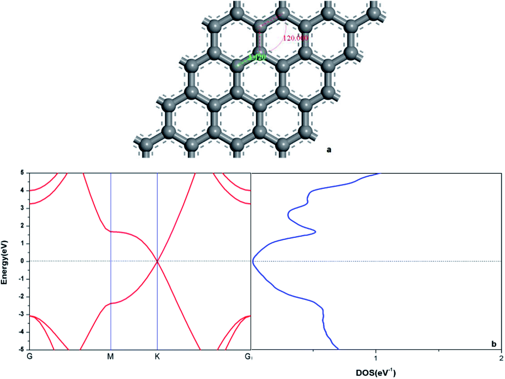 | ||
| Fig. 1 The geometric structure (a), band structure (b: left), and electron density of state (b: right) of graphene. | ||
 | ||
| Fig. 2 The geometric structures and Mulliken charges of doped graphenes: B-G (a), Al-G (b), Si-G (c), Ge-G (d), As-G (e), and Sb-G (f). | ||
| Systems | Charge (eV) | Band length (nm) | |||||
|---|---|---|---|---|---|---|---|
| X | C1 | C2 | C3 | X–C1 | C1–C2 | C2–C3 | |
| OG | 0 | 0 | 0 | 1.420 | 1.420 | ||
| B-G | 0.610 | −0.220 | 0.010 | 0.020 | 1.503 | 1.420 | 1.478 |
| Al-G | 2.120 | −0.620 | −0.050 | −0.090 | 1.764 | 1.424 | 1.642 |
| Si-G | 1.800 | −0.560 | −0.010 | −0.090 | 1.684 | 1.435 | 1.546 |
| Ge-G | 1.510 | −0.430 | −0.030 | −0.120 | 1.740 | 1.434 | 1.576 |
| As-G | 0.920 | −0.240 | −0.040 | −0.070 | 1.875 | 1.421 | 1.497 |
| Sb-G | 0.990 | −0.250 | −0.050 | −0.090 | 2.109 | 1.423 | 1.494 |
3.2 Population analysis
To explore the effects of geometric structures on the electronic and optical properties, the Mulliken charge analysis is performed first on the basis of the optimized structures. As shown in Fig. 2(a), B atom carries 0.610e charge and the charge of the ortho, meta, and para C atoms around B atom is −0.220e, 0.010e, and 0.020e, respectively, suggesting that the meta and para C atoms lose a few electrons and the ortho C atom gains a lot of electrons. It should be due to the fact that both the electronegativity and covalent radius of B (2.04 and 85 pm) atom is close to that of C (2.55 and 75 pm) atom, resulting in more charge transfers between B and ortho C atom compared to the meta and para C atoms. For Al-G, the charge of Al atom is 2.120e and Al transfers −0.620, −0.050, and −0.090e charges to its ortho, meta, and para C atoms (Fig. 2(b)), suggesting that Al and C atoms are electron donors and acceptors, respectively. Moreover, the meta and para C atoms get less electrons than ortho C atom. Similarly, this phenomenon also occurs in the Si, Ge, As, and Sb doped graphenes, illustrating that Si, Ge, As, and Sb atoms are also electron donors. As a result, the orders of the lost charges for the dopant atoms are as follows: Al (2.120) > Si (1.800) > Ge (1.020) > Sb (0.990) > As (0.920) > B (0.610), suggesting that Al and Si atoms lose more electrons than B, As, Ge, and Sb atoms. This difference can be attributed to the smaller electronegativity of Al (1.61) and Si (1.90) atoms than that of C atom, and the other atoms have similar electronegativity with C atom. Furthermore, the position of the dopant atoms in the graphene may also play an important role, which will be explored in future studies.The electron density difference can visually exhibit the ability of atomic charge transfer.42,50 As shown in Fig. 3, red and blue regions indicate the electron enrichment and electron scarcity, respectively. For OG, the electrons are uniformly distributed around the bonds of graphene's six-membered ring. After B, Al, Si, As, Ge, and Sb doping, the area of electron coverage is larger than that of pure graphene, indicating that electron transfer occurs between dopant atoms and C atoms. For B-G, the electron density around B atoms is slightly decreased compared with OG. Similarly, the same is also true for the electron density around meta and para C atoms. On the contrary, the electron density around ortho C atom near B atom is significantly increased, suggesting that most of electrons transfer to the ortho C atom from B atom compared with that of the meta and para C atoms. For the other doped graphenes, the electron density around dopant atoms is drastically reduced. Moreover, the electron densities around ortho C are much more than those around meta and para C atoms, indicating that the dopant atoms transfer more electrons to ortho C atoms.
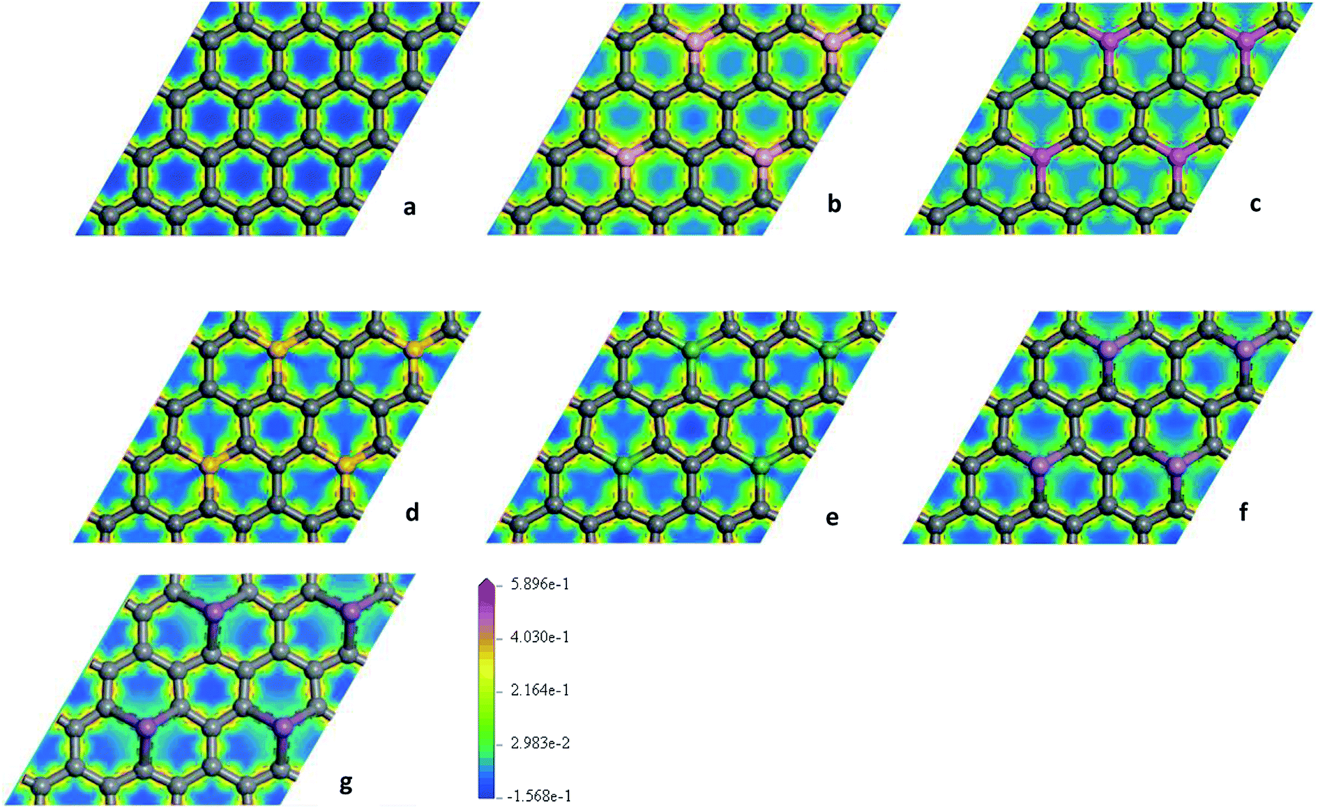 | ||
| Fig. 3 The electron density difference maps for OG (a), B-G (b), Al-G (c), Si-G (d), Ge-G (e), As-G (f), and Sb-G (g), respectively. | ||
3.3 Electronic properties
The band structure analyses of B-G (a), Al-G (b), Si-G (c), Ge-G (d), As-G (e), and Sb-G (f) are shown in Fig. S1 (left).† It is found that the introduction of dopant atoms open the band gap of graphene. Compared with OG, B, Al, and Sb doping makes the energy level curves move to the high energy, resulting in the Fermi level (E = 0) to pass through the valence band (Fig. S1(a, b, and f)†). On the contrary, for Si-G, As-G, and Ge-G, the highest energy level curves of the valence band nearly approach the Fermi level. Meanwhile, the energy level curves of the conduction band move up to higher Fermi energy (EF) (Fig. S1(c, d, and e)†). This phenomenon can also be proved by the analyses of the density of states (DOS) as shown in Fig. S1 (right).† For B-G (Fig. S1(a)†), the band gap is 0.663 eV, which is consistent with the result obtained by Nath et al.41 Fig. S1(b)† shows that the band gap of Al doped graphene is 1.480 eV, which is larger than that of the Al-doped graphene with 3.13% atomic concentration (0.40 eV).40 In our study, the atomic concentration of Al is 12.5%, indicating that the band gaps of doped graphenes are affected by the dopant concentration. Fig. S1(c)† shows that the band gap of Si-G is 0.783 eV, which is close to the previous studies.23,24 As shown in Fig. S1(d),† the band gap of Ge-G is 0.698 eV, where the band gap of Ge-doped graphene with 3.13% atomic concentration is 0.20 eV.30 As for As-G and Sb-G (Fig. S1(e and f)†), the band gaps of them are 0.682 and 1.583 eV, respectively, suggesting that the addition of sufficient numbers of dopant atoms can effectively open the band gap of graphene. Note that Sb-G has the largest band gap among all the doped graphenes although Sb atom do not lose more electrons than Al, Si, and Ge atoms. As a result, the orders of the band gaps for the doped graphenes are as follows: Sb-G (1.583) > Al-G (1.480 eV) > Si-G (0.783 eV) > Ge-G (0.698 eV) > As-G (0.682 eV) > B-G (0.663 eV).Subsequently, the influences of the external electric field (Ef) on the electronic properties of doped graphenes have been discussed, where the electric field is perpendicular to the doped graphenes surface. As shown in Fig. 4, the band gaps of B-G, Si-G, and Ge-G decrease with the changes of Ef from −0.4 to 1.2 eV Å−1. As for the band gap of Al-G, it increases first and then decreases. On the contrary, the band gaps of As-G and Sb-G increase with the changes of Ef from −0.4 to 1.2 eV Å−1. In details, the band gaps of the doped graphenes under the external electric fields from −0.4 to 1.2 eV Å−1 have been summarized in Table 2.
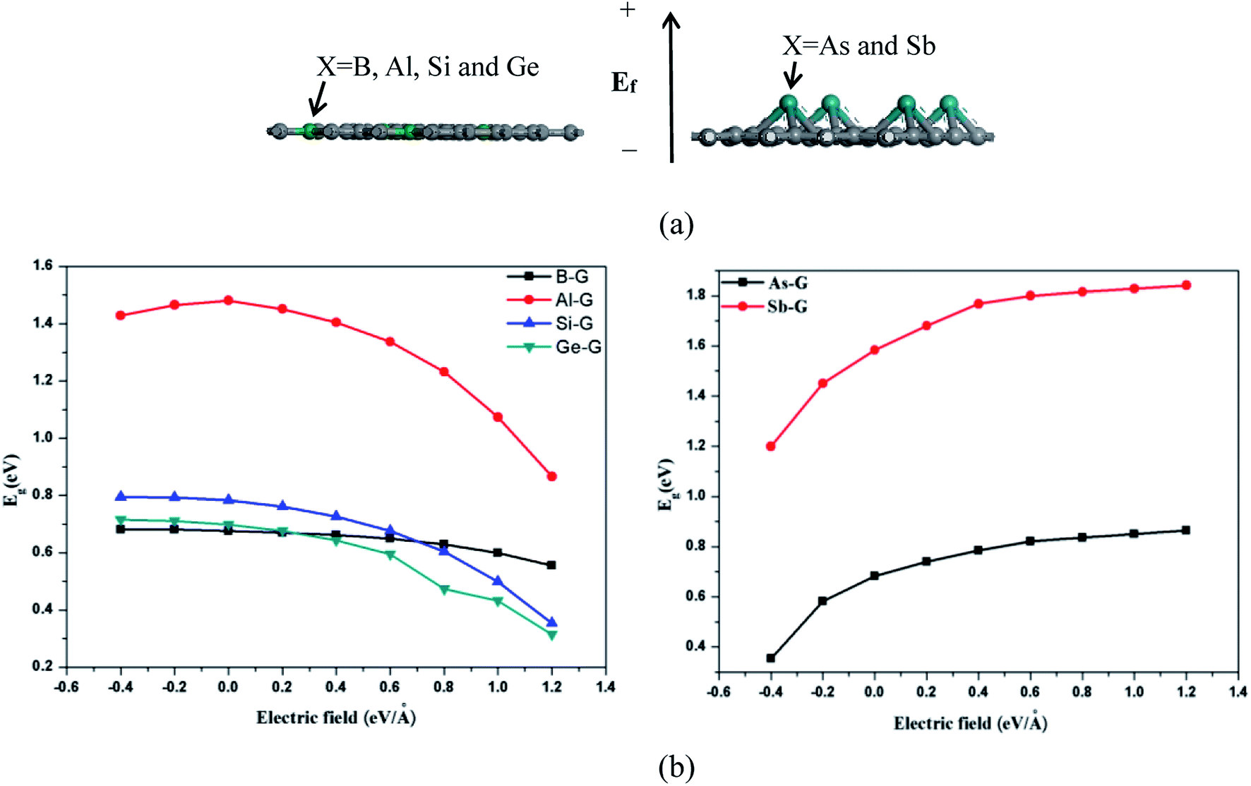 | ||
| Fig. 4 The sketch map of doped graphenes under the external electric field (Ef) (a), and the band gap (Eg) of doped graphene as a function of the electric fields (b), where Ef is introduced along z direction and the upward Ef is defined as positive labeled with symbol “+”. | ||
| System | Eg (eV) | ||||||||
|---|---|---|---|---|---|---|---|---|---|
| −0.4 | −0.2 | 0 | 0.2 | 0.4 | 0.6 | 0.8 | 1.0 | 1.2 | |
| B-G | 0.681 | 0.681 | 0.676 | 0.670 | 0.662 | 0.649 | 0.629 | 0.600 | 0.556 |
| Al-G | 1.428 | 1.465 | 1.481 | 1.451 | 1.405 | 1.337 | 1.232 | 1.074 | 0.866 |
| Si-G | 0.795 | 0.793 | 0.783 | 0.761 | 0.727 | 0.677 | 0.604 | 0.499 | 0.354 |
| Ge-G | 0.715 | 0.711 | 0.698 | 0.676 | 0.643 | 0.595 | 0.473 | 0.433 | 0.314 |
| As-G | 0.354 | 0.582 | 0.682 | 0.741 | 0.786 | 0.821 | 0.835 | 0.850 | 0.864 |
| Sb-G | 1.20 | 1.450 | 1.583 | 1.680 | 1.768 | 1.80 | 1.815 | 1.828 | 1.841 |
To further explore the effect of Ef on the electronic properties of the doped graphenes, the representative DOS of Al-G and Sb-G has been explored. As shown in Fig. 5, the DOS of the doped graphenes has been influenced irrespective of the positive or negative electric fields. For Al-G, the Fermi energy measured from the top of the valence bands and bottom of the conduction bands slightly moves downward to the Fermi level under the Ef from 0 to −0.4 eV Å−1. Moreover, the migration of the conduction bands is faster than that of the valence bands, resulting in the decrease of the band gap of Al-G with the increase of Ef. On the contrary, under the Ef from 0 to 0.4 eV Å−1, the energy of the valence bands and conduction bands moves upward to higher energy level and shift away from the Fermi level. Moreover, the migration of the valence bands is faster than that of the conduction bands, leading to the decrease of the band gap with the increase of Ef. Therefore, the external electric field will reduce the band gap of Al-G. As shown in Fig. 5(b), for Sb-G under the Ef from 0 to −0.4 eV Å−1, the energy of the valence bands has no obvious changes and the energy of the conduction bands moves downward to the Fermi level, resulting in the decrease of the band gap with the increase of Ef. However, the band gap of Sb-G is increased with the increase of Ef from 0 to 0.4 eV Å−1, which may be due to the fact that the energy of the conduction bands moves upward to higher energy level. Therefore, the band gap of Sb-G increases and decreases with the increase of the intensity of positive and negative electric fields, respectively. Probably, these phenomena may be related to the charge distributions on the doped graphenes. To clarify this point, the electron density difference maps for Al-G and Sb-G have been constructed. As shown in Fig. 6, the charge distribution is obviously affected by the electric field. For Al-G (Fig. 6(a)), despite the fact that the whole system has more uniformly distributed electrons under the electric field, the difference of charge between Al and C atoms is not obvious, indicating that the electric fields induce a weak dipole moment. So the band gap of Al-G is decreased under the external electric field. For Sb-G (Fig. 6(b)), under negative electric fields, the amounts of charge transfer between Sb and C atoms are less than that of zero field case. But under positive electric fields, more electron charges are transferred to C atoms around Sb atoms. These phenomena show that the positive electric fields have certain contributions to open the band gap of Sb-G.
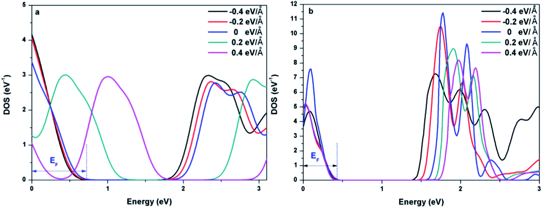 | ||
| Fig. 5 DOS of Al-G (a) and Sb-G (b) under different external electric fields. | ||
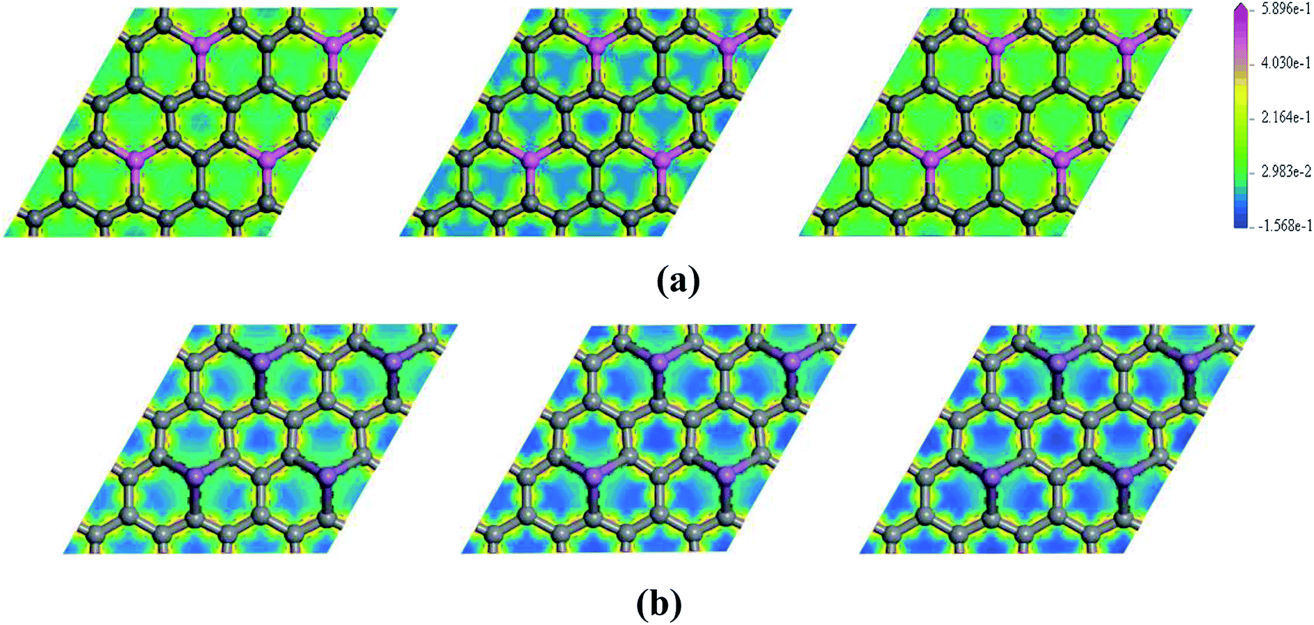 | ||
| Fig. 6 The electron density difference maps for Al-G (a) and Sb-G (b), where the map from left to right is plotted for Ef = −0.4, 0, 0.4 eV Å−1. | ||
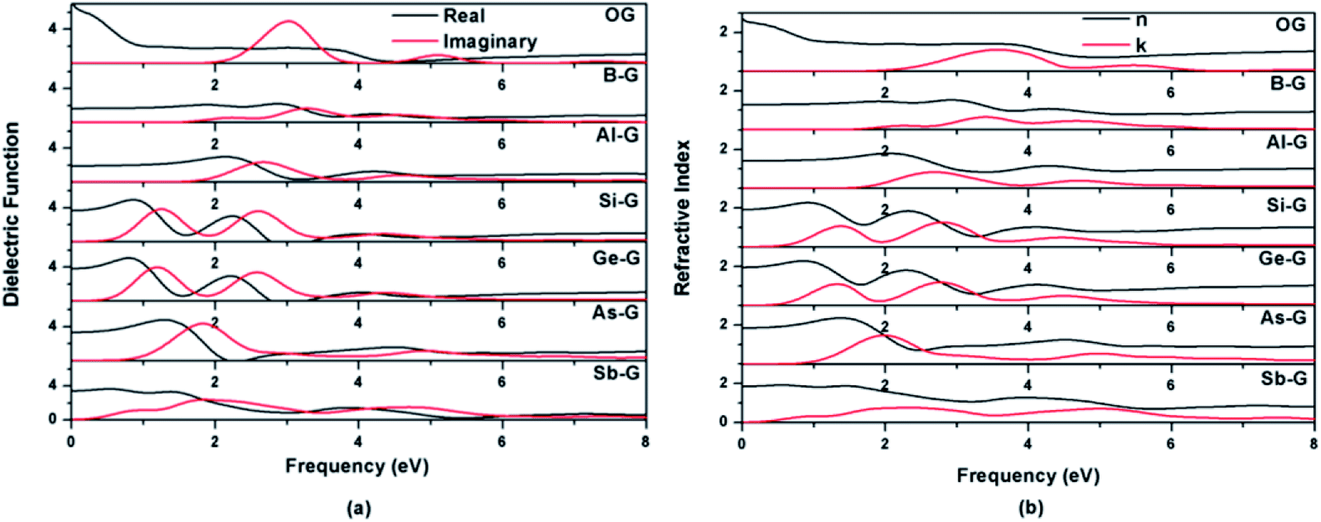
3.4 Optical properties
To explore the influences of the geometric structure on the optical properties, the absorption spectra, complex dielectric function, complex refractive index, and loss function (smearing = 0.2 eV) of OG and doped graphenes have been analyzed, where parallel electromagnetic wave polarization to sheet are taken into account. According to the optical selection rules, only π → π* (long wavelength or low frequency region) and σ → σ* (short wavelength or high frequency region) transitions are allowed. As a result, the curves of optical properties of OG and doped graphenes are similar with the results of previous studies. Here, the minor differences should be attributed to the different sizes of supercell, concentration of doped atom, k-point mesh, and smearing values employed in the calculations.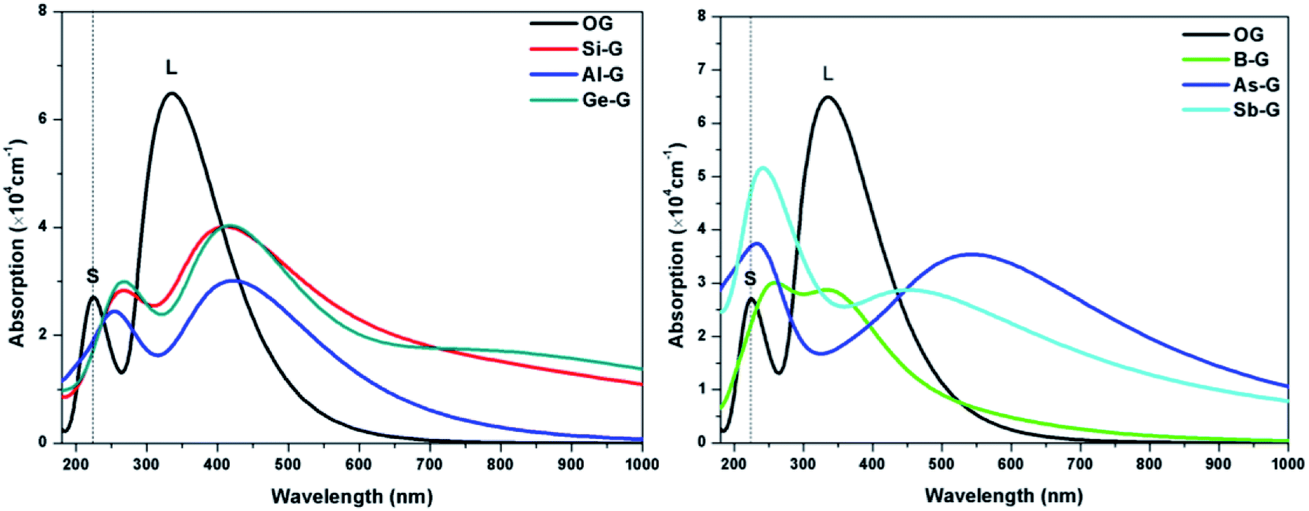 | ||
| Fig. 7 The absorption spectra of OG, B-G, Al-G, Si-G, Ge-G, As-G, and Sb-G. | ||
For B-G, the intensity of S peak is stronger compared with that of OG and its maximum value appears at 255 nm, suggesting that S peak shifts toward the long wavelength. However, L peak of B-G lies at 347(2.87 × 104 cm−1) nm, implying that there was no significant changes except for the decrease in peak strength, which is line with the result of Nath et al.41 For Al-G, S and L peaks appear at 257(2.42 × 10⁴) and 404(3.04 × 104 cm−1) nm, respectively, implying that the Al dopant can result in red shift for absorption peaks of graphene. These values are close to the values reported by Zhao et al.40 Moreover, the intensity of L peak is stronger than that of S peak, implying that π → π* transitions is stronger than σ → σ* transitions during the orbital transition of Al-G system. Especially, the same is also true for the peaks of Si-G and Ge-G, where S/L peaks of them are located at 267(2.83 × 10⁴)/412(4.01 × 104) and 227(5.65 × 10⁴)/531(3.96 × 104 cm−1) nm, respectively, which are close to Rafique and Kheyri's results.24,30 For As-G, S and L peaks are located at 227(5.65 × 10⁴) and 541(3.96 × 10⁴) nm, respectively, suggesting that S and L peaks occur red shift and the intensity of S peak is stronger than that of graphene. Interestingly, S peak becomes a sharp peak compared with L peak, suggesting that σ → σ* transitions is stronger than π → π* transitions during the orbital transition of As-G. Similarly, this phenomenon can also be observed for Sb-G. Here, S and L peaks are located at 246(5.01 × 10⁴) and 454(2.87 × 104 cm−1) nm, respectively. As a result, the absorption peaks of doped graphenes shift toward the long wavelength and their intensities are weaker than that of pure graphene. Comparatively speaking, the S peak intensities of Al-G, Si-G, and Ge-G are weaker than those of L peak. However, the opposite is true for the B-G, As-G, and Sb-G.
Fig. 8 presents the absorption spectra of doped graphenes under Ef ranging from −0.4 to 1.2 eV Å−1. Obviously, the external electric fields have significant influences on the optical properties of B-G, Al-G, Si-G, and Ge-G. The higher the Ef, the more obvious the red shift of L peaks of B-G, Al-G, Si-G, and Ge-G. Moreover, the S peaks gradually disappear. Therefore, the external electric field may contribute to π → π* transitions especially under the higher Ef. For example, as shown in Fig. 8(a), the intensity of L peak for B-G has no significant changes after applying Ef, but L peak appears at 345, 338, 332, 338, 350, 367, 395, 440, and 492 nm under −0.4, −0.2, 0.0, 0.2, 0.4, 0.6, 0.8, 1.0, and 1.2 eV Å−1, respectively. It implies that L peaks are red-shifted obviously with the increase of Ef independent of the direction of the electric field. Similarly, this phenomenon can also be observed for Al-G. As shown in Fig. 8(b), the L peaks of Al-G are shifted from 420(0.0), then 435(−0.4), 430(−0.2), 424(0.2), 435(0.4), 457(0.6), 482(0.8), and 500(1.0) to 482 nm (1.2 eV Å−1), implying that the absorption spectra of Al-G are transferred from the purple region to blue region by the applied external electric field. Furthermore, the intensity of L peaks has been strengthened under the negative electric field direction. For Si-G system, as shown in Fig. 8(c), its L peaks are located at 429(4.19 × 10⁴), 419(4.25 × 10⁴), 417(4.24 × 10⁴), 424(4.16 × 10⁴), and 443(4.04 × 104 cm−1) nm under −0.4, −0.2, 0.2, 0.4, and 0.6 eV Å−1, respectively. Therefore, the intensities of L peak are stronger than that of the zero electric field irrespective of the direction of the electric field, suggesting that the lower electric field may enhance the ability of π → π* transitions. On the other hand, L peaks are shifted from 470(3.82 × 10⁴) to 600(2.50 × 104 cm−1) nm when Ef ranges from 0.8 to 1.2 eV Å−1, suggesting that the higher electric field makes the spectra of Si-G into the yellow region. For Ge-G, as shown in Fig. 8(d), the external electric field makes the L peak intensity decrease independent of the direction of the electric field. Meanwhile, L peaks are red-shifted from 417(0.0), then 431(−0.4), 422(−0.2), 420(0.2), 431(0.4), 457(0.6), 49(0.8), and 551(1.0) to 620 nm (1.2 eV Å−1), implying that the absorption spectra of Ge-G have been transferred from the purple region to the orange region by applying the external electric field. Surprisingly, the absorption spectra of As-G and Sb-G exhibit the opposite phenomena. As shown in Fig. 8(e), the position of S peak of As-G has no obvious changes except the intensity of peak. L peaks fluctuate around 541 nm with the same intensity independent of the variation of the positive Ef. Under the negative Ef, the intensity of L peak decreases significantly. Similarly, as shown in Fig. 8(f), external electric field has only a slight effect on the intensity of the absorption peak of Sb-G. Probably, this point can be due to the fact that the degree of the migration for the valence band and conduction band under the external electric field is relatively small as shown in Fig. 5(b).
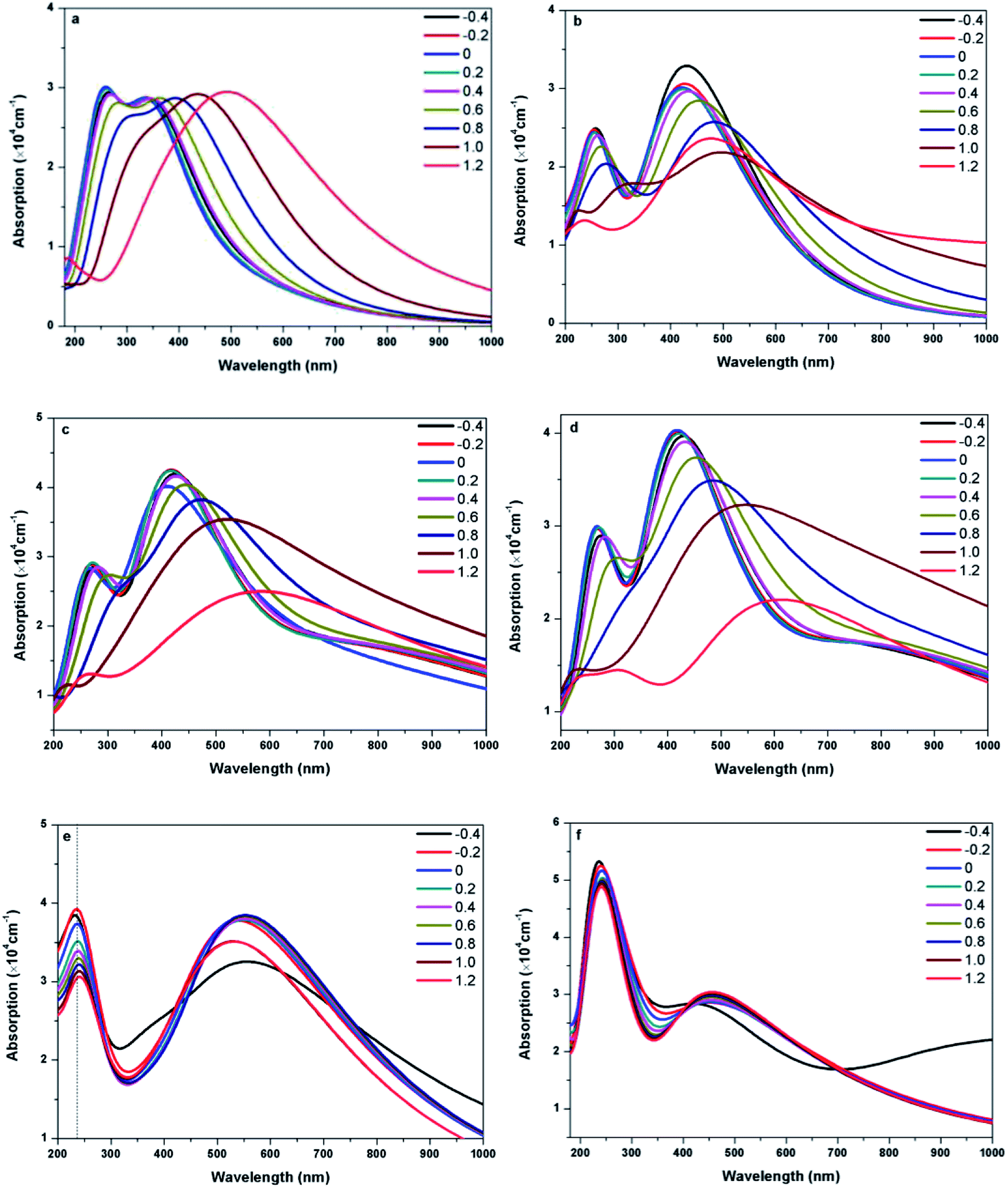 | ||
| Fig. 8 The absorption spectra of B-G (a), Al-G (b), Si-G (c), Ge-G (d), As-G (e), and Sb-G (f) under different Ef ranging from −0.4 to 1.2 eV Å−1. | ||
 | ||
| Fig. 9 Dielectric functions (a) and refractive indexes (b) of OG, B-G, Al-G, Si-G, Ge-G, As-G, and Sb-G. | ||
As shown in Fig. 9(b), the features of the refractive index of the doped graphenes are similar with that of dielectric function. The n0 values of B-G, Al-G, Si-G, Ge-G, As-G, and Sb-G are 1.28, 1.40, 1.91, 1.95, 1.84, and 1.85 eV, respectively, indicating that the n0 values of doped graphenes are smaller than that of OG. Meanwhile, doped graphenes also show obvious peaks of k(ω), corresponding to the peaks of ε2(ω). In the 0–4 eV, the gentle peaks of B-G and Sb-G are located at 2.25 and 2.36 eV, respectively. The strong peaks occur at 2.68 eV for Al-G, 1.38 and 2.80 eV for Si-G, 1.33 and 2.78 eV for Ge-G, and 2.0 eV for As-G, respectively.
Fig. S2† shows the dielectric functions of doped graphenes under Ef ranging from −0.4 to 1.2 eV Å−1. The real part of dielectric function (ε1(0)) of doped graphenes at zero frequency are given in Table 3. Obviously, the ε1(0) values of B-G, Al-G, Si-G, and Ge-G increase with the increase of Ef independent of the direction of the electric field. Moreover, as shown in Fig. S2,† the peak positions of the imaginary part of dielectric function for B-G, Al-G, Si-G, and Ge-G move toward low frequency under the same Ef. For As-G and Sb-G, the ε1(0) values slowly increase and then decrease from −0.4 to 1.2 eV Å−1, where a maximum value appears at 1.0 eV Å−1. As for the imaginary part of dielectric function, it is similar to that of the real part. Overall, these results indicate that the applied electric field may contribute to the increase of the dielectric constant of B-G, Al-G, Si-G, and Ge-G except for As-G and Sb-G, which can be attributed to the fact that the applied electric field facilitates π → π* transitions of B-G, Al-G, Si-G, and Ge-G compared with As-G and Sb-G. Moreover, this phenomenon has also been reflected from the analyses of refractive index and loss function of doped graphenes under the external electric field.
| System | External electric field (eV Å−1) | |||||||||
|---|---|---|---|---|---|---|---|---|---|---|
| −0.4 | −0.2 | 0 | 0.2 | 0.4 | 0.6 | 0.8 | 1.0 | 1.2 | ||
| B-G | ε1(0) | 1.68 | 1.66 | 1.65 | 1.67 | 1.70 | 1.76 | 1.85 | 2.02 | 2.34 |
| n(0) | 1.29 | 1.29 | 1.29 | 1.29 | 1.30 | 1.33 | 1.36 | 1.42 | 1.53 | |
| Al-G | ε1(0) | 3.33 | 2.49 | 1.90 | 1.99 | 2.02 | 2.07 | 2.22 | 2.70 | 5.06 |
| n(0) | 1.83 | 1.58 | 1.41 | 1.41 | 1.42 | 1.44 | 1.48 | 1.64 | 2.25 | |
| Si-G | ε1(0) | 3.69 | 3.65 | 3.65 | 3.73 | 3.86 | 4.12 | 4.54 | 5.44 | 5.78 |
| n(0) | 1.92 | 1.91 | 1.91 | 1.93 | 1.97 | 2.03 | 2.13 | 2.33 | 2.41 | |
| Ge-G | ε1(0) | 3.84 | 3.79 | 3.81 | 3.88 | 4.03 | 4.32 | 4.82 | 6.53 | 4.42 |
| n(0) | 1.96 | 1.95 | 1.95 | 1.97 | 2.01 | 2.08 | 2.20 | 2.55 | 2.10 | |
| As-G | ε1(0) | 3.11 | 3.35 | 3.40 | 3.47 | 3.51 | 3.53 | 3.35 | 3.29 | 3.28 |
| n(0) | 1.76 | 1.83 | 1.84 | 1.86 | 1.87 | 1.88 | 1.83 | 1.81 | 1.81 | |
| Sb-G | ε1(0) | 3.40 | 3.41 | 3.42 | 3.48 | 3.50 | 3.50 | 3.51 | 3.52 | 3.28 |
| n(0) | 1.20 | 1.85 | 1.85 | 1.87 | 1.768 | 1.87 | 1.87 | 1.88 | 1.88 | |
Fig. S3† shows the refractive indexes of doped graphenes under the applied electric field. Compared with the results without electric field, some changes of their peak positions and peak intensities occur. Namely, the curves of them tend to lower frequency with stronger intensity.
As show in Fig. S5,† the peaks of B-G and Al-G shift toward low frequency with decreasing intensity from −0.4 to 1.2 eV Å−1. For Si-G and Ge-G, their peaks move toward low frequency with decreasing intensity from −0.4 to 0.8 eV Å−1 and there is only a gentle peak in the range of 1.0–1.2 eV Å−1. For As-G and Sb-G, there are no noticeable changes for their peak positions and intensities.
4. Conclusions
In this study, the electronic and optical properties of B, Al, Si, Ge, As, and Sb doped graphenes have been detailedly investigated by using DFT method in the absence and presence of the external electric field. The results illustrate that the band gap of B-G, Al-G, Si-G, Ge-G, As-G, and Sb-G is 0.676, 1.481, 0.783, 0.698, 0.682, and 1.583 eV, respectively. After applying the external electric field, the band gaps of B-G, Al-G, Si-G, and Ge-G are decreased with the increase of the external electric field intensity. On the contrary, for As-G and Sb-G, the band gaps of them have been increased and reached 0.864 and 1.841 eV under 1.2 eV Å−1, respectively.As for the absorption spectra, red shifts occur for B-G (347 nm), Al-G (404 nm), Si-G (412 nm), Ge-G (513 nm), As-G (531 nm), and Sb-G (454 nm) compared with that of graphene without the external electric field. Moreover, the peak positions of dielectric function, refractive index, and loss function of doped graphenes are moved toward low frequency region. The real part of dielectric function (ε1(0)) and refractive index (n0) of doped graphenes at zero frequency are smaller than that of pure graphene. After applying the external electric field, the absorption spectra of B-G, Al-G, Si-G, and Ge-G are shifted to longer wavelengths of visible light with the increase of the electric field intensity. Meanwhile, the peak positions of dielectric function, refractive index, and loss function of doped graphenes are moved toward lower frequency region. For As-G and Sb-G, the external electric field can not almost change the peak positions of the absorption spectra, dielectric function, refractive index, and loss function. It is expected that the present results of the properties of these doped graphenes will be beneficial to their applications in the field of optoelectronics.
Conflicts of interest
There are no conflicts to declare.Acknowledgements
This work is supported by National Natural Science Foundation of China (21577076), Natural Science Foundation of Shandong Province (No. ZR2018MB020), the Project of Shandong Province Higher Educational Science and Technology Program (SK201504), and High Performance Computing Center of Qufu Normal University.References
- K. S. Novoselov, A. K. Geim, S. V. Morozov, D. Jiang, Y. Zhang, S. V. Dubonos, I. V. Grigorieva and A. A. Firsov, Electric field effect in atomically thin carbon films, Science, 2004, 306, 666–669 CrossRef CAS PubMed.
- K. S. Novoselov, A. K. Geim, S. V. Morozov, D. Jiang, M. I. Katsnelson, I. V. Grigorieva, S. V. Dubonos and A. A. Firsov, Two-dimensional gas of massless Dirac fermions in graphene, Nature, 2005, 438, 197–200 CrossRef CAS PubMed.
- C. W. J. Beenakker, Colloquium: Andreev reflection and Klein tunneling in graphene, Rev. Mod. Phys., 2008, 80, 1337–1354 CrossRef CAS.
- A. H. Castro Neto, F. Guinea, N. M. R. Peres, K. S. Novoselov and A. K. Geim, The electronic properties of graphene, Rev. Mod. Phys., 2009, 81, 109–162 CrossRef CAS.
- S. D. Sarma, S. Adam, E. H. Hwang and E. Rossi, Electronic transport in two dimensional graphene, Rev. Mod. Phys., 2011, 83, 407–470 CrossRef.
- R. R. Nair, P. Blake, A. N. Grigorenko, K. S. Novoselov, T. J. Booth, T. Stauber, N. M. R. Peres and A. K. Geim, Fine structure constant defines visual transparency of graphene, Science, 2008, 320, 1308 CrossRef CAS PubMed.
- A. A. Balandin, S. Ghosh, W. Bao, I. Calizo, D. Teweldebrhan, F. Miao and C. N. Lau, Superior thermal conductivity of single-layer graphene, Nano Lett., 2008, 8, 902–907 CrossRef CAS PubMed.
- B. Luo, B. Wang, X. L. Li, Y. Y. Jia, M. H. Liang and L. J. Zhi, Graphene-confined Sn nanosheets with enhanced lithium storage capability, Adv. Mater., 2012, 24, 3538–3543 CrossRef CAS PubMed.
- C. H. Xu, B. H. Xu, Y. Gu, Z. G. Xiong, J. Sun and X. S. Zhao, Graphene-based electrodes for electrochemical energy storage, Energy Environ. Sci., 2013, 6, 1388–1414 RSC.
- C. Lee, X. D. Wei, J. W. Kysar and J. Hone, Measurement of the elastic properties and intrinsic strength of monolayer graphene, Science, 2008, 321, 385–388 CrossRef CAS PubMed.
- G. Eda and M. Chhowalla, Chemically derived graphene oxide: towards large-area thin-film electronics and optoelectronics, Adv. Mater., 2010, 22, 2392–2415 CrossRef CAS PubMed.
- X. Huang, Z. Zeng, Z. Fan, J. Liu and H. Zhang, Graphene-based electrodes, Adv. Mater., 2012, 24, 5979–6004 CrossRef CAS PubMed.
- Q. Hu, X. Wu, Z. Yin and H. Zhang, Graphene-based electronic sensors, Chem. Sci., 2012, 3, 1764–1772 RSC.
- L. Wang, Z. Sofer, P. Simek, I. Tomandl and M. Pumera, Boron-doped graphene: scalable and tunable p-type carrier concentration doping, J. Phys. Chem. C, 2013, 117, 23251–23257 CrossRef CAS.
- R. Lv, Q. Li, A. R. Botello-Mendez, T. Hayashi, B. Wang, A. Berkdemir and Q. Hao, Nitrogen-doped graphene: beyond single substitution and enhanced molecular sensing, Sci. Rep., 2012, 2, 586 CrossRef PubMed.
- A. Fukushima, A. Sawairi, K. Doi, M. Senami, L. Chen, H. Cheng and A. Tachibana, Role of an aluminum atom on graphene for hydrogen adsorption, J. Phys. Soc. Jpn., 2011, 80, 074705 CrossRef.
- P. A. Denis, Band gap opening of monolayer and bilayer graphene doped with aluminium, silicon, phosphorus, and sulfur, Chem. Phys. Lett., 2010, 492, 251–257 CrossRef CAS.
- D. Gonzalez Larrude, Y. Garcia-Basabe, F. Lazaro Freire Jr and M. L. M. Rocco, Electronic structure and ultrafast charge transfer dynamics of phosphorous doped graphene layers on a copper substrate: a combined spectroscopic study, RSC Adv., 2015, 5, 74189–74197 RSC.
- S. Yang, L. Zhi, K. Tang, X. Feng, J. Maier and K. Müllen, Efficient synthesis of heteroatom (N or S)-doped graphene based on ultrathin graphene oxideporous silica sheets for oxygen reduction reactions, Adv. Funct. Mater., 2012, 22, 3634–3640 CrossRef CAS.
- Z. Wang, P. Li, Y. Chen, J. He, W. Zhang, O. G. Schmidt and Y. Li, Thiophene–sulfur doped reduced graphene oxide: synthesis, structure, and electrical properties, Nanoscale, 2014, 6, 7281–7287 RSC.
- L. Wei, G. L. Liu, D. Zh. Fan and G. Y. Zhang, Density functional theory study on the electronic structure and optical properties of S absorbed graphene, Phys. B, 2018, 545, 99–106 CrossRef CAS.
- Y. Zou, F. Li, Z. H. Zhu, M. W. Zhao, X. G. Xu and X. Y. Su, An ab initio study on gas sensing properties of graphene and Si-doped graphene, Eur. Phys. J. B, 2011, 81, 475–479 CrossRef CAS.
- M. Houmad, H. Zaari, A. Benyoussef, A. E. Kenz and H. Ez-Zahraouy, Optical conductivity enhancement and band gap opening with silicon doped graphene, Carbon, 2015, 94, 1021–1027 CrossRef CAS.
- M. Rafique, Y. Shuai and N. Hussain, First-principles study on silicon atom doped monolayer graphene, Phys. E, 2018, 95, 94–101 CrossRef CAS.
- Z. Jin, H. Nie, Z. Yang, J. Zhang, Z. Liu, X. Xu and S. Huang, Metal-free selenium doped carbon nanotube/graphene networks as a synergistically improved cathode catalyst for oxygen reduction reaction, Nanoscale, 2012, 4, 6455–6460 RSC.
- P. A. Denis, Chemical reactivity and band-gap opening of graphene doped with gallium, germanium, arsenic, and selenium atoms, ChemPhysChem, 2014, 15, 3994–4000 CrossRef CAS.
- R. J. Toh, H. L. Poh, Z. Sofer and M. Pumera, Transition metal (Mn, Fe Co, Ni)-doped graphene hybrids for electrocatalysis, Chem.–Asian J., 2013, 8, 1295–1300 CrossRef CAS PubMed.
- J. Zhao, Q. Deng, A. Bachmatiuk, G. Sandeep, A. Popov, J. Eckert and M. H. Rümmeli, Free-standing single-atom-thick iron membranes suspended in graphene pores, Science, 2014, 343, 1228–1232 CrossRef CAS.
- A. W. Robertson, B. Montanari, K. He, J. Kim, C. S. Allen, Y. A. Wu, J. Olivier, J. Neethling, N. Harrison, A. I. Kirkland and J. H. Warner, Dynamics of single Fe atoms in graphene vacancies, Nano Lett., 2013, 13, 1468–1475 CrossRef CAS PubMed.
- A. Kheyri, Z. Nourbakhsh and E. Darabi, Effect of Fe, Co, Si and Ge impurities on optical properties of graphene sheet, Thin Solid Films, 2016, 612, 214–224 CrossRef CAS.
- Z. Sofer, O. Jankovsky, P. Simek, K. Klimova, A. Mackova and M. Pumera, Uraniumand thorium-doped graphene for efficient oxygen and hydrogen peroxide reduction, ACS Nano, 2014, 8, 7106–7114 CrossRef CAS PubMed.
- E. Cruz-Silva, F. López-Urías, E. Muñoz-Sandoval, B. G. Sumpter, H. Terrones, J. C. Charlier, V. Meunier and M. Terrones, Electronic transport and mechanical properties of phosphorus- and phosphorus–nitrogen-doped carbon nanotubes, ACS Nano, 2009, 3, 1913–1921 CrossRef CAS PubMed.
- X. Ma, G. Ning, C. Xu and J. Gao, Phosphorus and nitrogen dual-doped few-layered porous graphene: a high performance anode material for lithium ion batteries, ACS Appl. Mater. Interfaces, 2014, 6, 14415–14422 CrossRef CAS PubMed.
- B. Feng, J. Xie, C. Dong, S. Zhang, G. Cao and X. Zhao, Graphite oxide to nitrogen and sulfur Co-doped few-layered graphene by a green reduction route via Chinese medicinal herbs, RSC Adv., 2014, 4, 17902–17907 RSC.
- P. A. Denis and C. Pereyra Huelmo, Structural characterization and chemical reactivity of dual doped graphene, Carbon, 2015, 87, 106–115 CrossRef CAS.
- M. M. Ervasti, Z. Fan, A. Uppstu, A. Krasheninnikov and A. Harju, Silicon and silicon-nitrogen impurities in graphene: structure, energetics and effects on electronic transport, Phys. Rev. B: Condens. Matter Mater. Phys., 2015, 92, 235412 CrossRef.
- S. Ullah, A. Hussain, W. Syed, M. A. Saqlain, I. Ahmad, O. Leenaerts and A. Karim, Band-gap tuning of graphene by Be doping and Be, B co-doping: a DFT study, RSC Adv., 2015, 5, 55762–55773 RSC.
- A. Hussain, S. Ullah and A. Farhan, Fine tuning the band-gap of graphene by atomic and molecular doping: a density functional theory study, RSC Adv., 2016, 6, 55990–56003 RSC.
- O. Olaniyan, E. Mapasha, D. Momodu, J. Madito, A. A. Khaleed, F. U. Ugbo, A. Bello, F. Barzegar, K. Oyedotun and N. Manyala, Exploring the stability and electronic structure of beryllium and sulphur Co-doped graphene: first principles study, RSC Adv., 2016, 6, 88392–88402 RSC.
- X. Zhou, C. H. Zhao, G. F. Wu, J. H. Chen and Y. Q. Li, DFT study on the electronic structure and optical properties of N, Al, and N-Al doped graphene, Appl. Surf. Sci., 2018, 459, 354–362 CrossRef CAS.
- P. Nath, S. Chowdhury, D. Sanyal and D. Jana, Ab-initio calculation of electronic and optical properties of nitrogen and boron doped graphene nanosheet, Carbon, 2014, 73, 275–282 CrossRef CAS.
- G. C. Loh and R. Pandey, A graphene-boron nitride lateral heterostructure – a first-principles study of its growth, electronic properties, and chemical topology, J. Mater. Chem. C, 2015, 3, 5918–5932 RSC.
- M. Y. Han, B. Ozyilmaz, Y. B. Zhang and P. Kim, Energy band-gap engineering of graphene nanoribbons, Phys. Rev. Lett., 2007, 98, 206805 CrossRef PubMed.
- Y. W. Son, M. L. Cohen and S. G. Louie, Half-metallic graphene nanoribbons, Nature, 2006, 44, 347–349 CrossRef PubMed.
- Y. Lu and J. Guo, Band gap of strained graphene nanoribbons, Nano Res., 2010, 3, 189–199 CrossRef CAS.
- G. Cocco, E. Cadelano and L. Colombo, Gap opening in graphene by shear strain, Phys. Rev. B: Condens. Matter Mater. Phys., 2010, 81, 241412 CrossRef.
- V. Hung Nguyen, et al., Disorder effects on electronic bandgap and transport in graphene-nanomesh-based structures, J. Appl. Phys., 2013, 113, 013702 CrossRef.
- P. Rani, G. S. Dubey and V. K. Jindal, DFT study of optical properties of pure and doped graphene, Phys. E, 2014, 62, 28–35 CrossRef CAS.
- R. Muhammad, Y. Shuai and H. P. Tan, First-principles study on hydrogen adsorption on nitrogen doped graphene, Phys. E, 2017, 88, 115–124 CrossRef CAS.
- X. Lu, X. Gao, J. Ren, C. Li, X. Guo, X. Yan and P. La, Effects of diverse metal adsorptions on the electronic and optical properties of the β-Si3N4 (2 0 0) surface: a first-principles study, Comput. Mater. Sci., 2018, 151, 296–306 CrossRef CAS.
Footnote |
| † Electronic supplementary information (ESI) available. See DOI: 10.1039/c9ra00326f |
| This journal is © The Royal Society of Chemistry 2019 |