
 Open Access Article
 This Open Access Article is licensed under a Creative Commons Attribution-Non Commercial 3.0 Unported Licence
Correlation between surface scaling behavior and surface plasmon resonance properties of semitransparent nanostructured Cu thin films deposited via PLD
Rahul Kesarwani,
Partha P. Dey and
Alika Khare *
*
Department of Physics, Indian Institute of Technology Guwahati, Guwahati, India. E-mail: alika@iitg.ac.in
First published on 12th March 2019
Abstract
The surface scaling behavior of nanostructured Cu thin films, grown on glass substrates by the pulsed laser deposition technique, as a function of the deposition time has been studied using height–height correlation function analysis from atomic force microscopy (AFM) images. The scaling exponents α, β, 1/z and γ of the films were determined from AFM images. The local roughness exponent, α, was found to be ∼0.86 in the early stage of growth of Cu films deposited for 10 minutes while it increased to 0.95 with a longer time of deposition of 20 minutes and beyond this, it was nearly constant. Interface width w (rms roughness) scales with depositing time (t) as ∼ tβ, with the value of the growth exponent, β, of 1.07 ± 0.11 and lateral correlation length ξ following ξ = t1/z and the value of 1/z = 0.70 ± 0.10. These exponent values convey that the growth dynamics of PLD Cu films can be best described by a combination of local and non-local models under a shadowing mechanism and under highly sticking substrate conditions. From the scaling exponents and power spectral density function, it is concluded that the films follow a mound like growth mechanism which becomes prominent at longer deposition times. All the Cu films exhibited SPR properties where the SPR peak shifts towards red with increasing correlation length (ξ) whereas bandwidth increases initially with ξ and thereafter decreases gradually with ξ.
1. Introduction
Surface roughness of a thin film plays a significant role in controlling the performance of various plasmonic, photonic and electronic devices.1–7 Surface roughness of coated optical components affects the performance and efficiency of optical resonators, high damage mirrors, solar cells, etc. aside from controlling the reflectivity.3,8 The electron mobility in the inversion layer of the metal-oxide-semiconductor (MOS) system is strongly influenced by surface roughness.9 Therefore, a quantitative characterization of the surface roughness is essential not only for assessment of fabrication processes, but also for precise evaluation of device preformation. The surface roughness of the thin films controls the amount of the incident light converted to heat energy which in turn controls the efficiency of some devices e.g. solar cells.10 The increase in surface roughness decreases the response time of biosensor whereas it increases the conversion efficiency of a solar cell.4,5 The nanostructured metallic thin films of Cu, Ag, Au etc. fabricated, onto the suitable dielectric (e.g. glass), exhibits the surface plasmons (SPs) phenomena at the interface.11–15 SPs forms the basis for near-field spectroscopy, surface enhanced Raman spectroscopy, enormously large data storage, sensor, solar cell etc.13,16 The SP behavior is governed by the dielectric properties of substrate and size and shape of the nanoparticles which in turn depends on type of surface growth and related parameters e.g. roughness, correlation length, the film growth mechanism etc.17–20 The SP signal is also affected by the roughness of the surfaces.21,22 The peak position of surface plasmon resonance (SPR) depends on the surface nanostructure.7 Thus, there is a dire need to assess the surface roughness of the nanostructured metal thin films in order to forecast its plasmonic properties as well as optical properties. The atomic force microscope (AFM) can be easily implemented to measure the surface roughness, correlation length and other growth exponents involved in the growth mechanism for thin films. It is a non-destructive, fast and accurate technique which is applicable for all types of the film including reflecting as well as nonreflecting, former of which can also be analyzed by optical techniques.9,23,24 From the analysis of surface morphology, its scaling behavior and growth model can be predicated ex situ which is not only helpful is understanding the nucleation process but also plays an important role in correlating with the physical properties of the thin film25–29 In the present work, surface scaling behavior of nano structured Cu thin films, grown onto the glass substrate at its softening temperature via pulsed laser deposition (PLD) technique, as a function of deposition time is presented. The height–height correlation function (HHCF) and power spectral density function (PSDF) were extracted from AFM images for the estimation of growth exponents α, β and 1/z. The influence of all these growth parameters on the plasmonic properties of semitransparent nanostructured Cu thin film is also presented.2. Experimental methods
Nanostructured Cu thin films were deposited onto polished glass substrate via PLD by focusing a 2nd harmonic of a Q-switched Nd:YAG laser (Quanta system HYL-01, pulse duration – 10 ns and repetition rate – 10 Hz) on polycrystalline Cu target of >99.965% purity (Sigma-Aldrich, U.S.A), at a laser fluence of ∼ 4 J cm−2 under vacuum (∼10−6 mbar).11 The films were deposited for 6, 8, 10, 20, 30 and 45 min duration at a substrate temperature of 400 °C. The thickness of these films were measured by profilometer (Veeco Dektak 150). All these six films were subjected to X-ray diffractometer (Rigaku TTRAX III) operated at a wavelength of 1.5407 Å of Cu Kα at a glancing incidence angle of ω = 1° and scanned 2θ in the range of 20° to 70° in an angular step of 0.02° for structural identification. In order to study the dynamic scaling behaviour and growth mechanism of Cu films via PLD technique, all these films were subjected to AFM (Agilent 5500). The Surface Plasmon Resonance (SPR) spectra of these thin metallic Cu films were recorded by UV-Vis-NIR spectrophotometer (Shimadzu UV 3100) and correlated with the scaling parameters.3. Results and discussions
The thickness of the PLD Cu thin film was found to increase nearly linearly with the deposition time. It was in the range of ∼35–280 nm for the deposition time of 6–45 minutes respectively.The XRD spectra of Cu metallic thin films deposited on the glass substrate for various deposition time from 6 to 45 minutes are shown in Fig. 1. The XRD peaks observed at 43.33° and 50.29° correspond to the Cu (111) and Cu (220) planes, respectively with former being more intense.30 Fig. 1 clearly shows the increase in the intensity of both the peaks with the deposition time which is due to the increase in thickness thus facilitating the participation of larger number of diffracting planes. The crystallite size was estimated from the FWHM of the most intense peak of (111) plane by Debye–Scherrer's formula.31 The inset in Fig. 1 shows the nearly linear increase in the size of Cu crystallites from 3.2 nm to 30.3 nm with increasing deposition time from 6 to 45 min respectively.
 | ||
| Fig. 1 XRD spectra of PLD Cu thin films deposited on glass substrate (SiO2) for deposition time, t, from 6 to 45 min. Inset shows variation of crystallite size with t. | ||
The surface morphology of the films was characterized by AFM to unveil the surface microstructures and the growth dynamics of the films.29 Fig. 2(a)–(f) shows the AFM images of all the films for the deposition time of 6, 8, 10, 20, 30 and 45 min, respectively. The initial visualization of AFM micrographs indicates the uniform distribution of grains over the film surface. Initially, for the lower deposition time, the grains were observed to be of spherical in shape. With increasing deposition time or growth time, the repeated impinging of particle flux from incoming laser induced plasma towards the substrate, the nucleation sites increased followed by coalescence of smaller size grains to form bigger particles along with the formation of columnar structure. Eventually, at 30 and 45 minutes duration, relatively large sized and densely packed grains were formed as is evident from Fig. 2(e) and (f) respectively. To unveil the growth process and the dynamic scaling behaviour, the scaling exponents; root mean square (RMS) roughness or interface width (w) and local slope (m) of the islands had been calculated from AFM images. These quantities were obtained from HHCF, H(r, t). It is defined by the statistical average of the mean square of height difference between the pair of points, separated by r and is written as:29
| H(r, t) = 〈|h(r + r′, t) − h(r′, t)|2〉 | (1) |
 | ||
| Fig. 2 AFM images of PLD Cu films for the deposition time of (a) 6 minutes, (b) 8 minutes, (c) 10 minutes, (d) 20 minutes, (e) 30 minutes and (f) 45 minutes. | ||
The HHCF, can also be defined by exponential correlation model, which satisfies the requirement for self-affine surface and manifests anisotropic scale invariance, given by29
 | (2) |
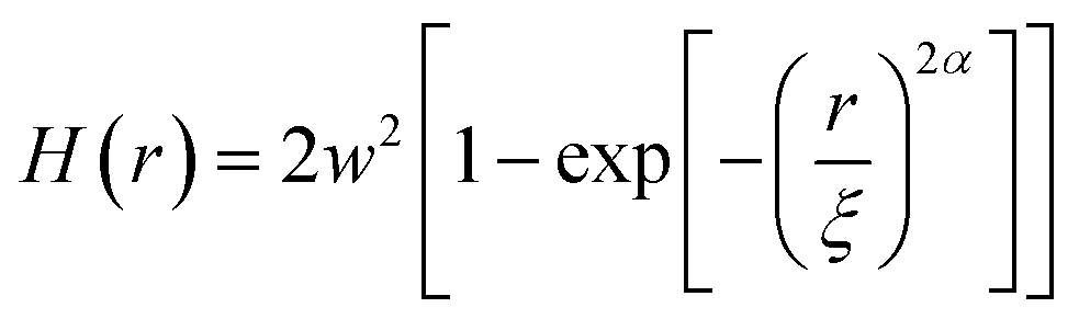
For r ≪ ξ, from eqn (2)
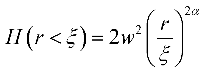 | (3) |
 | (4) |
The log–log plot of H(r, t) as measured from AFM images, as a function of distance ‘r’ along with curve fitted to eqn (2) for all the films deposited for various interval of time (t) is shown in Fig. 3. The measured value fits well to eqn (2) (R2 > 0.97). The HHCF can be clearly divided into two distinct regions of r ≪ ξ and r ≫ ξ. For longer deposition time of 20–45 minutes, an oscillatory behavior was observed for r ≫ ξ indicating the formation of the mounded surface.29 It is clear from Fig. 3 that the value of H(r, t) increases as Cu film thickness increases (with increasing growth time), indicating the increase in the RMS roughness. From the best fitting of experimental HHCF curves using eqn (2), w, ξ as well as α were estimated for each film. The variation of w, ξ and α as a function of deposition time on the log–log scale is shown in Fig. 4 (a), (b) and (c) respectively. Fig. 4(a) shows the increase in the value of w from 0.65 to 7.48 nm for the films grown from 6 to 45 minutes respectively further confirming the increase in roughness of the film with the increasing growth time ‘t’.
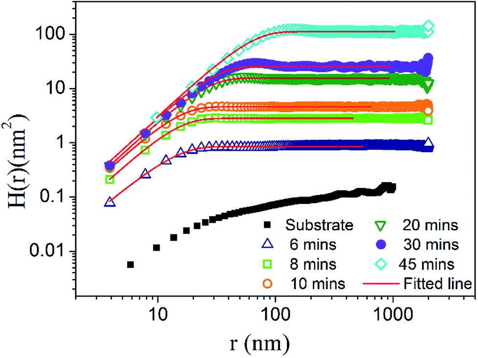 | ||
| Fig. 3 log–log plot of HHCF, H(r, t) as a function of distance r and fitted to eqn (2) for Cu thin films on glass substrate for deposition times of 6–45 minutes along with bare substrate. | ||
 | ||
| Fig. 4 Variation in (a) surface roughness w, (b) correlation length ξ, and (c) roughness exponent α with the deposition duration, t. | ||
The increasing nature of ξ with t, as shown in Fig. 4(b), indicates the lateral growth of the islands. The lateral growth could be attributed to the increased in crystallite size (XRD results, Fig. 1) with increasing deposition time. The parameters w and ξ showed power law dependence as w ∼ tβ and ξ ∼ t1/z respectively having values of β = 1.07 ± 0.11 and z = 1.42 ± 0.21. There is a slight decrease in value of α from 0.88 for 6 minutes deposited film to 0.86 for that of 10 minutes and beyond this it increases to 0.95 for 20 minutes and thereafter the changes are insignificant. This affirms that local roughness decreases while the RMS roughness (defined by w) increases from 0.65 to 7.48 nm with increasing film thickness from ∼35 to 280 nm. In order to quantify the dynamics of the roughness, ξ versus w for all the samples were plotted (on log–log scale) and shown in Fig. 5(a). The relation between w and ξ can be worked out as w ∼ ξγ, where the value of exponent, γ, was found to be 1.50 ± 0.54 comparable to that obtained from the values of β and 1/z. The value of γ can predict the competition between lateral and vertical growth.
 | ||
| Fig. 5 Plot of (a) w versus ξ and (b) local slope m as a function of deposition time, t. | ||
The observed value of γ > 1 indicates the faster vertical growth compared to lateral growth and is also related to the roughness of the film surface. In order to identify the mode of the growth, local slope 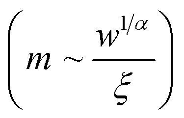 as a function of deposition time was plotted and as shown in Fig. 5(b). The dependence of m on time indicates the non-stationary growth in the present case. The upward shift of the H(r) with deposition time, Fig. 3, further signifies the non-stationary growth of the film.25,29
In the case of PLD, the particle flux from laser produced plasma impinging on the substrate is of diverging nature having non-uniform distribution of particles thus the growth process is dominated by shadowing effect. Another unique feature of this technique is the large kinetic energy of the particles striking the substrate, and so the deposition can be performed at relatively low substrate temperature with minimal re-emission.32 Thus growth model best suited for the PLD is of that of proposed by Drotar et al. in which the surface under shadowing (roughening effect) and zeroth-order sticking coefficient corresponding to minimal reemission (s0 = 1 and sn = 0 for n > 0) are considered. It is described by stochastic continuum growth equation,33
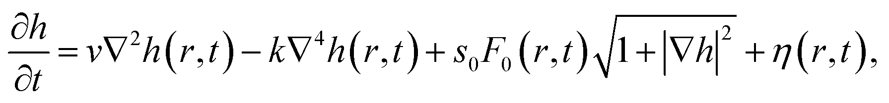 | (5) |
The first term on the right-hand side (v∇2h) represents the evaporation dynamics where surface relaxation is achieved by annealing mechanism, the second term (k∇4h) accounts for smoothening by surface diffusion due to the curvature-induced chemical potential gradient, in the third term F0 contains information about the shadowing effect, as well as the nature of the incoming particle flux given by  where θ is the local polar angle, Φ is the local azimuthal angle and R(θ, Φ) is the distribution of the incoming flux and
 ![[n with combining circumflex]](https://www.rsc.org/images/entities/i_char_006e_0302.gif) is the unit vector normal to the substrate. The factor
is the unit vector normal to the substrate. The factor  in the third term represents growth normal to the local surface and the last term in eqn (5), η (r, t), is the noise in the system. The value of β and 1/z via Monte Carlo simulations in 2 + 1 dimensions from the eqn (5) was reported to be 1 and 0.93 ± 0.1 respectively.33 These values are in close proximity to that of obtained in the present case for HHCF analysis. In the PLD process, the impinging particles from laser produced plasma plume on the substrate, arrive within the angular range of 0° to ±θ1/2(∼cos−1(1/2)p),34 where θ1/2 is the angle between normal to the target surface and the direction where flux density becomes half of maximum and p varies from 7–20 depending on laser spot size on the target, laser fluence and degree of ionization of plasma.32,34 In the present work, on Cu target the laser spot size was of ∼1 mm diameter and laser fluence ∼ 4 J cm−2, the corresponding value of p ∼ 7–8 giving θ1/2–22–23°.34 The glass substrate used has a melting point of around 550 °C and deposition temperature was kept at 400 °C, close to the softening temperature, which could have resulted in a very high sticking coefficient, s0 ∼ 1. These deposition conditions favouring large shadowing and high sticking coefficient for substrate satisfy the requirement for the surface growth model given by eqn (5).33 Under the dynamic scaling, Δ = β/α − 1/z = 0, but in the present case, Δ = 0.37 indicates the presence of anomalous scaling behavior and the surface is not self-affine. This is understandable as the growth of the film in PLD is under strong influence of shadowing and thus dynamic scaling no longer holds.35 Interestingly, the calculated exponents (α, β, 1/z) are quite close to the exponents predicted by the model of mound formation.33,36 The oscillating behavior of the HHCF in the region where r ≫ ξ, Fig. 3, also indicates the formation of mounded surface, particularly for thicker films (deposited for duration, t = 20, 30 and 45 minutes).
The power spectral density function (PSDF), given by  29 for these films is exhibited in Fig. 6. It displays P(k) versus k plot extracted from the respective AFM images of Cu films deposited on glass substrates for duration of 6, 8, 10, 20, 30 and 45 minutes. The PSDF shows a characteristics peak, km = 2π/λ (λ = wavelength) for mounded surface and is absent for self-affine surface.29 The characteristic peak was absent in the PSDF spectra of the films deposited for 6 to 10 minutes duration, Fig. 6(a)–(c), indicating self-affine film surface. The PSDF of the films deposited for duration longer than 10 minutes show characteristics peak depicting mound formation. With increasing time, the peak feature of mounded surface becomes more prominent and km (∼1/ξ) reduces indicating increase in average separation between the islands. Inset in Fig. 6 shows corresponding 2D fast Fourier transform (FFT) images. It clearly shows a bright ring like structure in k-space for films deposited for longer times, 30 and 45 minutes, further supporting the mound growth.28 From above observation it is clear that the growth of the Cu film initially, for the shorter duration of deposition is predominantly self-affine surface but as deposition progresses film surface becomes mounded with the well-defined characteristic wavelength. The formation of mounds on any surface are basically due to different growth effects such as step-edge barrier, diffusion effect, shadowing, and re-emission, and which could be local or non-local in nature. In the present case, the non-local phenomena of strong shadowing owing to the directional nature of PLD along with high sticking condition of substrate (the deposition performed at glass softening temperature) favours mound formation in Cu films.
 | ||
| Fig. 6 PSDF, P(k) as a function of k (in reciprocal space) for Cu thin films deposited on glass substrate for the deposition time of (a) 6 minutes, (b) 8 minutes, (c) 10 minutes, (d) 20 minutes, (e) 30 minutes and (f) 45 minutes. Inset shows corresponding 2D FFT pattern of the AFM images. | ||
Metal nanoparticles (NPs) having plasmonic properties possess characteristic SPR peak at which incident light is strongly absorbed or scattered. Fig. 7(a) shows the absorption spectra of Cu films grown for deposition time from 6 minutes to 45 minutes via PLD. All these spectra exhibit the characteristic SPR absorption peak with asymmetric tail toward longer wavelength and broad bandwidth. All these absorbance spectra were fitted with bi-gaussian lineshape function37 and are shown in Fig. 7(a) as solid lines for estimation of SPR peak positions and respective bandwidths (Γ). The SPR peak, λSPR, shifts to longer wavelength side and accompanied by continuous increase in intensity with increasing time of deposition. The SPR peak position as a function of ξ and w are shown in Fig. 7(b) and (c) respectively. It was observed that with increase in ξ, which gives island size, λSPR was red shifted from 780 nm to 922 nm. According to Mie theory,38 metal clusters above a critical size exhibit red-shift in λSPR, with increasing size of cluster.15 The surface roughness, w, of the film is also responsible for the shift in λSPR and it increases with w7 and similar trend was observed in the present case as shown Fig. 7(c).
 | ||
| Fig. 7 (a) The absorption spectra of PLD Cu thin film, (b) SPR peak positions (λSPR) as a function of correlation length (ξ), (c) λSPR as a function of interface width and (d) bandwidth (Γ) as a function of correlation length (ξ). | ||
The broadening of the SPR bandwidth increases abruptly initially from 428 nm to 635 nm with ξ increasing from 13 to 14.5 nm respectively and then it falls down to 470 nm with further increase in ξ to 58 nm as shown in Fig. 7(d). The broadening of SPR band as well as asymmetric nature are due to wide size distribution of nanoparticles within the film, irregularity in the shapes, and increase in surface roughness of the film.14,39,40 The bandwidth of SPR has been reported to increase with decreasing particle size exhibiting inverse size effect15 while it increases in proportion to r.m.s roughness.39,41 In the present case, SPR bandwidth increased for the films deposited from 6 minutes to 10 minutes due to increase in interface width (or r.m.s roughness) from 0.6 nm to 1.51 nm even though ξ increased from 13 to 14.5 nm. However, the film deposited for 20 min to 45 min (ξ > 20 nm) had shown an overall decrease in SPR bandwidth with an increase in ξ from 24 to 58 nm satisfying the inverse size effect. Thus w and ξ play dominant role in shaping up the SPR bandwidth of the plasmonic nanostructured Cu thin films.
4. Conclusions
The evolution of nanostructured Cu thin films deposited onto glass substrate via PLD at 400 °C substrate temperature as a function of increasing deposition time was investigated. The film thickness was ranging from 35 nm to 280 nm for the deposition time of 6 to 45 minutes respectively. The XRD spectra showed the dominating peak corresponding to Cu (111) and relatively week peak corresponding to Cu (220) with average crystallite size increasing from 3.6 to 29.5 nm with increasing deposition time. From HHCF analysis (obtained from AFM images), the interface width (RMS roughness), w, was observed to scale with depositing time (t) as, ∼t1.07±0.11 while lateral correlation length ξ grows as t0.70±0.10 affirming the faster vertical growth compared to the lateral growth. The average roughness exponent α was observed to be nearly 0.95. The results showed that shadowing instability model for deposition with no remission can explain the growth of PLD Cu films onto SiO2. The strong shadowing effect is attributed to directional nature of PLD. The high sticking probability was due to the deposition taking place at around softening temperature of the substrate. From the analysis of PSDF and 2D FFT, the evolution of the PLD Cu films follows strong shadowing assisted mound-like growth. The anomalous scaling behavior of growth exponent was observed for the films of higher thickness. All the Cu films exhibited SPR peaks where the peak intensity increased with increasing thickness. The peak position and bandwidth of SPR, show the dependent on the correlation length ξ and RMS roughness w estimated from HHCF function.Conflicts of interest
There are no conflicts of interest to declare.Acknowledgements
The Central Instrument Facility (CIF), IIT Guwahati is acknowledged for providing the atomic force microscope.References
- A. V. Zayats, I. I. Smolyaninov and A. A. Maradudin, Phys. Rep., 2005, 408, 131–314 CrossRef CAS.
- Y.-H. Kim, S.-H. Kwon, H.-S. Ee, Y. Hwang, Y.-S. No and H.-G. Park, J. Opt. Soc. Korea, 2016, 20, 188–191 CrossRef CAS.
- Y.-C. Chung, P.-J. Cheng, Y.-H. Chou, B.-T. Chou, K.-B. Hong, J.-H. Shih, S.-D. Lin, T.-C. Lu and T.-R. Lin, Sci. Rep., 2017, 7, 39813 CrossRef CAS PubMed.
- K. M. Byun, S. J. Yoon and D. Kim, Appl. Opt., 2008, 47, 5886–5892 CrossRef CAS PubMed.
- V. E. Ferry, L. A. Sweatlock, D. Pacifici and H. A. Atwater, Nano Lett., 2008, 8, 4391–4397 CrossRef CAS PubMed.
- D. A. Polonyankin, A. I. Blesman and D. V. Postnikov, J. Phys.: Conf. Ser., 2017, 830, 012112 CrossRef.
- M. Kanso, S. Cuenot and G. Louarn, J. Opt. A: Pure Appl. Opt., 2007, 9, 586 CrossRef.
- M. Sato, S. Kajita, R. Yasuhara, N. Ohno, M. Tokitani, N. Yoshida and Y. Tawara, Opt. Express, 2013, 21, 9333–9342 CrossRef CAS PubMed.
- T. Yoshinobu, A. Iwamoto and H. Iwasaki, Jpn. J. Appl. Phys., 1994, 33, 383 CrossRef CAS.
- Ľ. Scholtz, L. Ladanyi and J. Müllerová, Advances in Electrical and Electronic Engineering, 2014, 12, 631 Search PubMed.
- R. Kesarwani and A. Khare, Appl. Phys. B: Lasers Opt., 2018, 124, 116 CrossRef.
- S. Law, V. Podolskiy and D. Wasserman, Nanophotonics, 2013, 2, 103–130 CAS.
- J. Zhang, L. Zhang and W. Xu, J. Phys. D: Appl. Phys., 2012, 45, 113001 CrossRef.
- V. N. Rai, A. K. Srivastava, C. Mukherjee and S. K. Deb, Appl. Opt., 2012, 51, 2606–2615 CrossRef CAS PubMed.
- S. Link and M. A. El-Sayed, Int. Rev. Phys. Chem., 2000, 19, 409–453 Search PubMed.
- R. Kesarwani, H. Chaturvedi and A. Khare, presented in part at the International Conference on Fiber Optics and Photonics 2016, Kanpur, December, 2016, DOI:10.1364/photonics.2016.P1A.18.
- J. P. Huang, L. Gao and Z. Li, Solid State Commun., 2000, 115, 347–352 CrossRef CAS.
- C. Noguez, J. Phys. Chem. C, 2007, 111, 3806–3819 CrossRef CAS.
- M. M. Miller and A. A. Lazarides, J. Phys. Chem. B, 2005, 109, 21556–21565 CrossRef CAS PubMed.
- M. Nasehnejad, G. Nabiyouni and M. G. Shahraki, J. Phys. D: Appl. Phys., 2017, 50, 375301 CrossRef.
- D. Lepage, D. Carrier, A. Jiménez, J. Beauvais and J. J. Dubowski, Nanoscale Res. Lett., 2011, 6, 388 CrossRef PubMed.
- C. Lee, C. S. Robertson, A. H. Nguyen, M. Kahraman and S. Wachsmann-Hogiu, Sci. Rep., 2015, 5, 11644 CrossRef CAS PubMed.
- H. Yoshino, A. Abbas, P. M. Kaminski, R. Smith, J. Walls and D. Mansfield, J. Appl. Phys., 2017, 121, 105303 CrossRef.
- T. V. Vorburger and E. Teague, Precis. Eng., 1981, 3, 61–83 CrossRef.
- J. H. Jeffries, J.-K. Zuo and M. Craig, Phys. Rev. Lett., 1996, 76, 4931 CrossRef CAS PubMed.
- G. Palasantzas and J. Krim, Phys. Rev. Lett., 1994, 73, 3564 CrossRef CAS PubMed.
- M. Pelliccione, T. Karabacak, C. Gaire, G.-C. Wang and T.-M. Lu, Phys. Rev. B, 2006, 74, 125420 CrossRef.
- S. M. Obaidulla and P. Giri, Appl. Phys. Lett., 2015, 107, 221910 CrossRef.
- M. Pelliccione and T.-M. Lu, Evolution of thin film morphology modeling and simulations, ISBN: 978-0-387-75108-5, Springer, Berlin, 2008 Search PubMed.
- V. Figueiredo, E. Elangovan, G. Goncalves, P. Barquinha, L. Pereira, N. Franco, E. Alves, R. Martins and E. Fortunato, Appl. Surf. Sci., 2008, 254, 3949–3954 CrossRef CAS.
- P. P. Dey and A. Khare, J. Alloys Compd., 2017, 706, 370–376 CrossRef CAS.
- D. Fork, D. Chrisey and G. Hubler, Pulsed Laser Deposition of Thin Films, ed. D. B Chrisey and G. K. Hubler, John Wiley and Sons, USA, 1994, vol. 16, pp. 407–412 Search PubMed.
- J. T. Drotar, Y.-P. Zhao, T.-M. Lu and G.-C. Wang, Phys. Rev. B: Condens. Matter Mater. Phys., 2000, 62, 2118 CrossRef CAS.
- I. Weaver and C. Lewis, J. Appl. Phys., 1996, 79, 7216–7222 CrossRef CAS.
- J. J. Ramasco, J. M. López and M. A. Rodríguez, Phys. Rev. Lett., 2000, 84, 2199 CrossRef CAS PubMed.
- J. H. Yao and H. Guo, Phys. Rev. E, 1993, 47, 1007 CrossRef.
- T. Buys and K. De Clerk, Anal. Chem., 1972, 44, 1273–1275 CrossRef CAS.
- Q. Fu and W. Sun, Appl. Opt., 2001, 40, 1354–1361 CrossRef CAS PubMed.
- G. Rasigni, F. Varnier, M. Rasigni, J. Palmari and A. Llebaria, Phys. Rev. B: Condens. Matter Mater. Phys., 1983, 27, 819 CrossRef CAS.
- L. M. Liz-Marzán, Langmuir, 2006, 22, 32–41 CrossRef PubMed.
- N. Fang, Z. Liu, T.-J. Yen and X. Zhang, Appl. Phys. A: Mater. Sci. Process., 2005, 80, 1315–1325 CrossRef CAS.
| This journal is © The Royal Society of Chemistry 2019 |