DOI:
10.1039/C8RA10614B
(Paper)
RSC Adv., 2019,
9, 7575-7586
Formation of polarization needle-like domain and its unusual switching in compositionally graded ferroelectric thin films: an improved phase field model†
Received
28th December 2018
, Accepted 13th February 2019
First published on 6th March 2019
Abstract
Compositionally graded ferroelectrics (cgFEs), which possess a spatial variation in material composition, exhibit anomalous or even unprecedented properties. Despite several breakthroughs having been achieved in experiments, there surprisingly is a lack of an effective simulation approach for cgFEs, thereby greatly hindering a deep understanding about underlying mechanisms hidden behind the observed phenomena. In this study, an improved phase field model is proposed for a cgFE made of PbZr(1−x)TixO3 based on the Ginzburg–Landau theory. The improved approach enables us to capture several key phenomena occurring in the cgFE PbZr0.8Ti0.2O3 ⇔ PbZr0.2Ti0.8O3 thin film that are observed from experiments, such as the formation of needle-like domains with curved domain walls, ferroelastic switching under an electric field, and the voltage offset of the hysteresis loop. Results obtained from the improved approach indicate that the high elastic energy near the needle-tip of an a-domain gives rise to a deflection of the domain wall from the regular a/c domain wall, while the high concentration of the depolarization field shrinks a part of the a-domain near the needle-tip and terminates the a-domain within the cgFE thin film. These facilitate the stabilization of needle-like domains with curved domain walls in the cgFE thin film. Furthermore, the flexoelectricity is proven to play an important role in the voltage offset of the hysteresis loop. On the other hand, the ferroelectric switching process in the cgFE thin film exhibits a vastly different response in comparison to that in homogeneous ferroelectric thin films, including local switching initiation and formation and annihilation of vortex–antivortex pairs during the switching. The present study, therefore, provides an incisive approach for investigations on cgFEs, which may bring new understanding and unique insights into these complex materials, as well as novel potential applications.
1 Introduction
Spontaneous breaking of spatial-inversion symmetry at the unit cell level results in the formation of a stable yet switchable electrical polarization in ferroelectrics, which, in turn, allows the materials to be applied across a broad range of advanced technologies, including nonvolatile random access memory (FeRAM) devices;1 sensors, actuators, and transducers;2 field-effect transistors;3,4 tunnel junctions;5 magnetoelectric-coupling devices;6,7 and switchable photovoltaics.8 Recently, an additional macroscopic broken spatial-inversion symmetry has been introduced into the system by using compositionally graded ferroelectric (cgFE) thin films, in which the chemical compositions are spatially varied throughout the thickness of the thin films. This macroscopic spatial-inversion symmetry breaking brings about novel physical properties, such as the presence of built-in electric fields,9 shifted hysteresis loops,9–12 large susceptibilities,13 and a potential for geometric frustration.14 Therefore, cgFEs have emerged as a potential candidate for novel applications in electric devices,15 and attracted considerable experimental and theoretical attention in the last decade.
Experimentally, it was reported early on that an offset in the vertical (polarization) axis of the hysteresis loop occurs in cgFE heterostructures, and the polarization gradients in the material were primarily believed to be the origin of the observed offsets.11,16 Later, an experimental investigation on the origin of hysteresis loop shifts in cgFEs9 indicated that the vertical offsets were explicitly dependent on the measurement circuit16,17 and the offsets should be along the horizontal (voltage) axis because of a built-in electric field. The origin of horizontal offsets results from the macroscopic broken spatial-inversion symmetry, and thereby, is intrinsic to the cgFE materials. Recently, a large horizontal offset of the ferroelectric hysteresis loop has been further demonstrated to originate from strong internal long-range electric fields that arise from compositional variations, by using high quality cgFE thin films.18 On the other hand, a high dielectric response over a wide temperature range has been reported for BaTiO3 cgFE thin films with altered Ba-site stoichiometry along the thickness.19–21 In these studies, the interesting characteristic overlays the broad and flat profile of the dielectric constant versus temperature, i.e., there is an absence of anomaly dielectric that is commonly observed in homogeneous ferroelectrics. The temperature independent dielectric constant originates from a strong smearing of the paraelectric–ferroelectric phase transition of the entire heterostructure accompanied by a reduction of the global transition temperature of the entire layer, with the highest Curie temperature due to the internal (depolarizing) electric fields. More recently, unexpected crystal and domain structures, and thereby novel properties, have been observed in cgFE thin films.22–24 These studies have demonstrated that large polarization gradients and desirable temperature-stable susceptibilities can be achieved through the control of composition and strain gradients in ferroelectrics.23 More interestingly, strain gradients in compositionally graded heterostructures made of PbZr(1−x)TixO3 can stabilize unusual needle-like ferroelastic domains that terminate inside the film.24 The stabilization of such a needle-like domain structure in a cgFE originates from complex interactions among the electrical and mechanical fields, and rendering intuitive guesses about these systems becomes quite difficult. Despite a significant scientific interest and an immense potential for applications, the structure–property relationships in cgFE thin films remain unclear since the physical mechanisms behind the observed behaviors, which arise from a plethora of intrinsic and extrinsic factors, have been difficult to identify. In turn, this has limited the adoption and utilization of cgFEs in advanced ferroelectric-based devices.
Theoretically, an attempt to understand the exotic properties in cgFEs has been preliminarily made with the use of transverse Ising models.25,26 Recent development in theoretical approach based on principles of non-linear thermodynamics can shed light on the polarization stabilities, phase transformation characteristics and dielectric properties of cgFEs.27–29 These theoretical studies provide an explanation as to why cgFEs should have lower dielectric losses and lower leakage currents compared to homogeneous ferroelectrics. In addition, role of the flexoelectric effect in the enhancement and stabilization of polarization components in cgFEs has also been demonstrated by using an extended thermodynamic theory.27,28,30 Although the use of theoretical approaches can explain some experimental observations, there still lacks a consideration of domain structures and their response to the mechanical and electric excitations, despite of their crucial roles in determination of macroscopic properties. This thus limits the use of theoretical methods for cgFEs, particularly with complex domain structures. On the other hand, the domain structure in cgFEs can be investigated using first-principles calculations.14 However, the heavy computational load imposes restrictions on the number of atoms and temperature in the simulation system that makes it critically difficult for further investigation on the behavior of polarization and domain structures in cgFEs under mechanical and electric fields. To circumvent these difficulties and to provide an effective approach for investigations on cgFEs, a distinct strategy is essential. As a potential alternative, phase field modeling based on the Ginzburg–Landau theory has been commonly used to study domain structures in ferroelectric materials, and polarization switching under a static electric field and/or mechanical loading.31–37 Although the phase field model is, until now, only developed for homogeneous ferroelectric systems, an integration of a non-linear thermodynamic formalism based on Ginzburg–Landau theory for the cgFE system into phase field frameworks is quite promising.
In this work, a new phase field model is developed for cgFE thin films made of PbZr(1−x)TixO3, which incorporates an extended non-linear thermodynamic formalism based on the Ginzburg–Landau theory. The developed phase field model is validated through an investigation on the formation of needle-like a-domains that have recently been experimentally observed in a cgFE PbZr0.8Ti0.2O3 (top) ⇔ PbZr0.2Ti0.8O3 (bottom) thin film.24 Based on the simulation results, the mechanism hidden behind the formation of needle-like a-domains with curved domain walls is unveiled. In addition, the ferroelastic and ferroelectric switching of the needle-like domain in the cgFE thin film are also investigated. Furthermore, the underlying mechanism for the voltage offset of the hysteresis loop that was observed in experiment is explored and discussed.
2 Computational details
2.1 Phase field model of cgFEs based on the Ginzburg–Landau theory
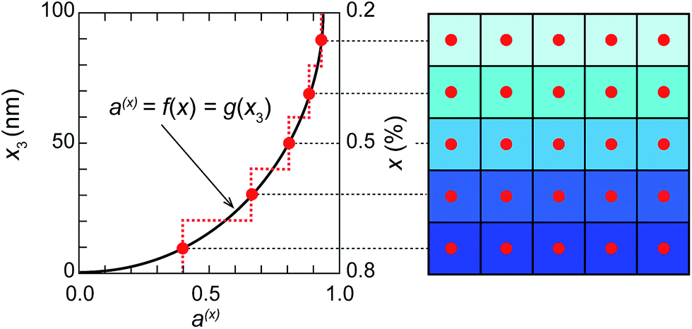
Here, we carry out the groundwork for an extension of the thermodynamic formalism for cgFEs based on the Ginzburg–Landau theory. To study PbZr(1−x)TixO3 (PZT), we have utilized a formalism expanded to the sixth order. The material parameters of cgFEs are functions of the mole fraction x of PbTiO3 in PZT, e.g., a(x) = f(x), where ax is any material parameter, such as thermodynamic stiffness coefficients, elastic compliance or stiffness, electrostrictive coefficients, and Curie temperature of the constitutive materials. x = 0 corresponds to the pure PbZrO3 material and x = 1 corresponds to the pure PbTiO3 ferroelectric. In the present study, the compositional materials are assumed to linearly vary along the thickness of the thin film; that is the x3 direction. Therefore, material parameters are also functions of the coordinate along thickness, a(x) = f(x) = g(x3). The schematic of the finite element model for the cgFE structure and the change of material properties along the x3 direction are provided in Fig. 1. A set of material parameters corresponding to a particular mole fraction x are assigned to an element layer depending on their coordinates in the x3 direction. The model, thus, strongly depends on the mesh sizes. To provide a good presentation for the cgFE model, small uniform meshing along the material gradation direction are required. In this study, uniform elements with the sizes of 0.4 nm in the thickness direction, which is as small as the PbTiO3 lattice constant,38 are employed.
 |
| | Fig. 1 Sketch outlining the gradual variation of material properties along the x3 coordinate as captured by the cgFE model. | |
The total free energy of the cgFE system, FFE, is essentially the sum of the free energies of each element layer, and is described as:
| |
 | (1) |
where
Vn is the volume of the
nth element layer,
fFE(x) is the total free energy density of ferroelectric with the mole fraction
x, and
m is the number of element layers to describe the gradation of material constituents.
fFE(x) is described by:
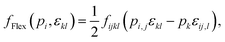
31–34,39| | |
fFE(x) = fL(x)(pi) + fG(pi,j) + fElas(x)(εij, pi) + fFlex(pi, εij) + fE(x)(pi, Ei), (i, j = 1, 2, 3)
| (2) |
where the superscript (
x) indicates that the functions are dependent of the mole fraction
x and spatially-dependent;
pi is a polarization vector;
pi,j = ∂
pi/∂
xj denotes the derivative of the
ith component of the polarization vector
pi, with respect to the
jth coordinate
xj;
εij and
Ei denote the components of strain and electric field, respectively.
fL(x)(
pi),
fG(
pi,j),
fElas(x)(
εij,
pi),
fFlex(
pi,
εij), and
fE(x)(
pi,
Ei) are the Landau energy density, the gradient energy density, the elastic energy density, the flexoelectric energy density, and the electrostatic energy density, respectively.
The Landau energy density is expanded in terms of polarization components up to the sixth order as:40–43
| |
 | (3) |
where
α1(x) is the dielectric stiffness, and
α11(x),
α12(x),
α111(x),
α112(x), and
α123(x) are higher order dielectric stiffness constants. The corresponding Landau coefficients are given by:
43–45| α11(x) = (10.612 − 22.655x + 10.955x2) × 1013/C0, |
| α111(x) = (12.026 − 17.296x + 9.179x2) × 1013/C0, |
| α112(x) = (4.2904 − 3.3754x + 58.804e−29.397x) × 1014/C0, |
| α123(x) = η2 − 3α111(x) − 6α112(x) |
where
T and
T0 denote the temperature and the Curie–Weiss temperature, respectively,
C0 denotes the Curie constant and
κ0 is the dielectric constant of a vacuum, which are given as:
43–45| η1 = [2.6213 + 0.42743x − (9.6 + 0.012501x) × e−12.6x] × 1014/C0, |
| η2 = [0.887 − 0.76973x + (16.255 − 0.088651x) × e−21.255x] × 1015/C0, |
| T0 = 462.63 + 843.4x − 2105.5x2 + 4041.8x3 − 3828.3x4 + 1337.8x5, |
The gradient energy density for ferroelectric materials represents the domain wall energy density that gives the energy penalty for the spatially inhomogeneous polarization. The gradient energy density is described by:46
| | |
fG(pi,j) = Gijklpi,jpk,l, (k, l = 1, 2, 3)
| (4) |
where
Gijkl are the gradient energy coefficients. In the present study, the gradient coefficients are assumed to be independent of the mole fraction
x, and equal to the values for PbTiO
3.
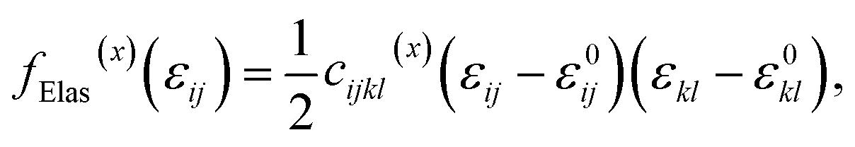
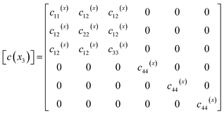
35,39 The elastic energy density induced by mechanical strain is given by:
31,43| |
 | (5) |
where
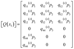
cijkl(x) are the elastic coefficients and
ε0ij =
Qijkl(x)pkpl is spontaneous strain or eigenstrain and
Qijkl(x) is the electrostrictive coefficient tensor. The elastic constants for a number of compositions are adopted from a previous study,
47 and are given in
Table 1. Note that, as the elastic coefficients slightly change with the change of mole fraction
x, the elastic coefficients of material with 0.2 ≤
x ≤ 0.4 adopt the values for
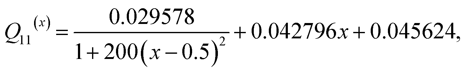
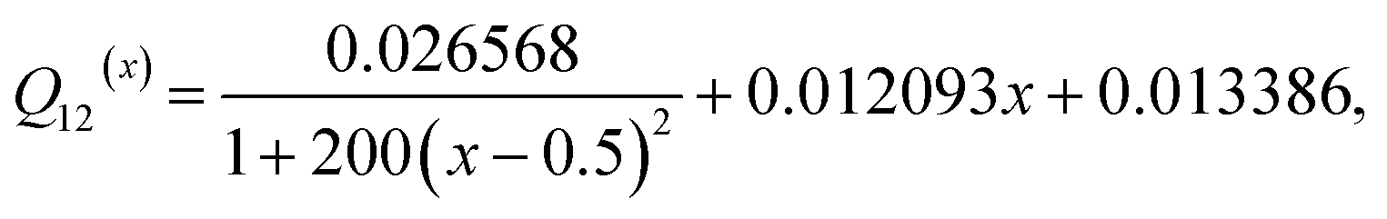
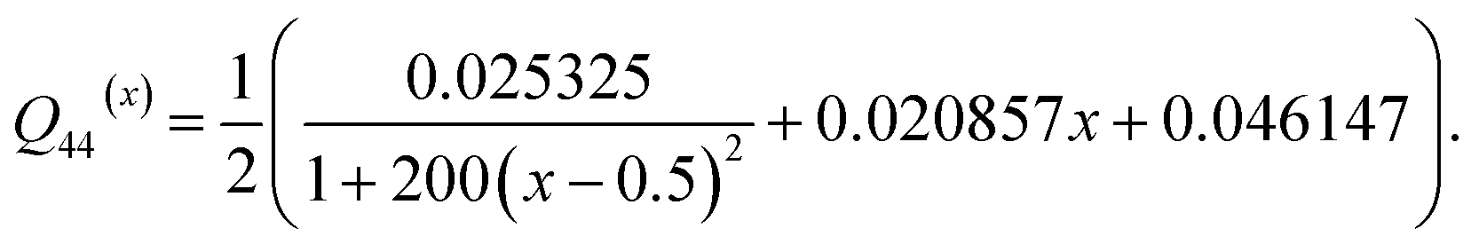
x = 0.4. For cubic symmetry, electrostrictive coefficients are given as:
43,45
Table 1 Elastic coefficients of PbZr(1−x)TixO3 for a number of compositions
| Ti content x |
0.4 |
0.5 |
0.6 |
0.7 |
0.8 |
0.9 |
1.0 |
| c11 (1011 N m−2) |
1.681 |
1.545 |
1.696 |
1.712 |
1.728 |
1.704 |
1.746 |
| c12 (1011 N m−2) |
0.826 |
0.840 |
0.819 |
0.811 |
0.802 |
0.760 |
0.7937 |
| c44 (1011 N m−2) |
0.406 |
0.348 |
0.472 |
0.571 |
0.694 |
0.833 |
1.111 |
Flexoelectricity, the electromechanical coupling between the polarization and strain gradient (direct effect) or mechanical stress and electric field gradient (converse effect), is a property of all insulators.48 The flexoelectric coupling energy density is expressed as:48–51
| |
 | (6) |
where
εij,l = ∂
εij/∂
xl and
fijkl are components of the flexocoupling tensor. The electrostatic energy density, which is obtained through Legendre transformation, is expressed as:
31,52| |
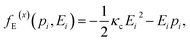 | (7) |
where
κc is the dielectric constant of the background material.
The temporal evolution of the polarization field towards its thermodynamic equilibrium state is described by the time-dependent Ginzburg–Landau (TDGL) equation:
| |
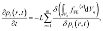 | (8) |
where
L is a kinetic coefficient,
r = (
x1,
x2,
x3) is the spatial vector, and
t denotes evolution time.
On the basis of Mindlin’s strain gradient theory53 the mechanical equilibrium equation accounting for contributions of strain gradients is described as:
| |
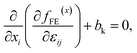 | (9) |
where
bk are the components of a body force per unit volume. The equilibrium of the electric field is governed by Maxwell’s (or Gauss’) equation as:
| |
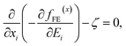 | (10) |
where
ζ is the volume charge density.
To solve the equilibrium equations, a numerical algorithm based on the finite element method (FEM) is employed in the present study. Using the variation or principle of virtual work, the weak form of the governing eqn (8)–(10) is expressed as:
| |
 | (11) |
where
ui is displacement;
ti and
ω are the surface traction and the surface charge, respectively;
ϕ is electrical potential; (∂
fFE(x)/∂
pi,j)
ξj denotes the surface gradient flux; and
ζj is the component of the normal unit vector of the surface. For the space discretization we use hexahedral elements, of which each node is assigned with seven degrees of freedom, including three polarization components, one electrical potential variable, and three displacement components. In comparison with the phase field model that uses the Fourier spectral iterative perturbation algorithm,
32,54 the phase field model based on the finite element algorithm does not require uniform hexahedral (3D) and quadrilateral (2D) meshes and periodic boundary conditions for numerical implementation.
55 The present phase field model is able to simulate ferroelectrics with arbitrary boundary conditions and geometrical shapes. Therefore, the phase field model with an FEM-based algorithm is suitable and effective for the study of domain evolution in cgFEs.
In general, the finite element stiffness equations can be written as:
where,
de = (
ue,
ϕe,
pe) are the degrees of freedom of an element in the cgFE system,
Ke is the tangent matrix, and
Fe denotes the load vector. The tangent matrix
Ke has a block structure and can be described as:
| |
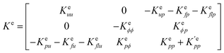 | (13) |
where,
here,
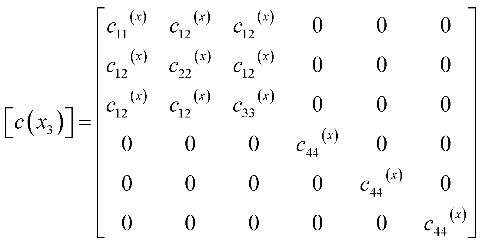
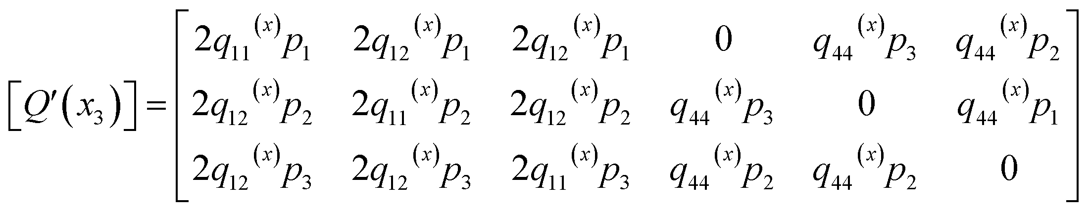
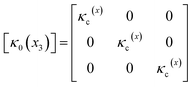
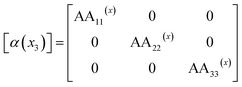
Ωe is the volume of an element. In the present work, the matrices [
c(
x3)], [
Q(
x3)], [
Q′(
x3)], [
κc(
x3)], and [
α(
x3)] are functions of spatial coordinates along the
x3 direction, which are distinguished from the previous phase field model for homogeneous ferroelectrics where all the functions are independent of the coordinates. Details of these matrices are provided below, while details of the remaining matrices are provided in previous studies.
56,57 Therefore, tangent matrix
Ke can be described for the spatial variation of material in cgFE systems.
| |
 | (14) |
| |
 | (15) |
where,
| q11(x) = c11(x)Q11(x) + 2c12(x)Q12(x), |
| q12(x) = c11(x)Q12(x) + c12(x)(Q11(x) + Q12(x)), |
| |
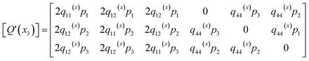 | (16) |
| |
 | (17) |
| |
 | (18) |
where,
| AA11(x) = 2α1(x) + 4α11(x)p12 + 2α12(x)(p22 + p32) + 6α111(x)p14 + α112(x)[4p12(p22 + p32) + 2(p24 + p34)] + 2α123(x)p22p32, |
| AA22(x) = 2α1(x) + 4α11(x)p22 + 2α12(x)(p12 + p32) + 6α111(x)p24 + α112(x)[4p22(p12 + p32) + 2(p14 + p34)] + 2α123(x)p12p32, |
| AA33(x) = 2α1(x) + 4α11(x)p32 + 2α12(x)(p12 + p22) + 6α111(x)p34 + α112(x)[4p32(p12 + p22) + 2(p14 + p24)] + 2α123(x)p12p22. |
Note that in the present study the thermodynamic formalism and the material coefficients of PbZr(1−x)TixO3 measured by M.J. Haun et al.41,44,45,58,59 are adopted into the phase field model for the cgFE thin film. Such thermodynamic formalism and material coefficients of PbZr(1−x)TixO3 have been widely used in phase field simulations and have yielded highly consistent results to experiment data.60,61 The thermodynamic formalism and the material coefficients of PbZr(1−x)TixO3 measured by M. J. Haun et al. are reliable and can be used to provide physical meanings for experimental observations. Therefore, it is reasonable to further employ the thermodynamic formalism and the material coefficients of PbZr(1−x)TixO3 in the phase field model of cgFEs, in order to reproduce the experimental data with support of the proper physics.
2.2 Simulation model and procedure
According to the previous experimental study,24 here we consider 100 nm-thick, linear compositionally graded PbZr0.8Ti0.2O3 (top) ⇔ PbZr0.2Ti0.8O3 (bottom) heterostructures. The simulation model is constructed with dimensions of 100 × 10 × 100 nm. We introduce a Cartesian coordinate system with the x1x2 plane coincident with the thin film plane and the x3 direction along the thin film thickness. The mechanical boundary condition on the bottom surface is: the node at the center is fixed and other nodes can only move in the x1 − x2 plane, such that the substrate strain can be relaxed by the applied field. Periodic boundary conditions are applied along the x1 and x2 axes. The spatial mesh of the simulation model is composed of 2.5 × 10⁵ hexahedral elements. The thin film consists of a linear cgFE with the [100], [010], and [001] crystallographic orientations along the x1, x2, and x3 directions, respectively.
The thermodynamic equilibrium of the polarization field in the cgFE thin film without external fields is obtained by starting from an initial paraelectric state with small random perturbations. The evolution of the polarization field is numerically simulated by iteratively solving the TDGL equation. A backward Euler scheme and Newton iteration method are used in the FEM algorithm for the time integration and nonlinear iteration, respectively. The polarization configuration is stably formed when an insignificant change in polarization is observed.
The electrical potential at the top and bottom surfaces is firstly set to zero to allow the film to reach equilibrium. After equilibrium is reached, electrical switching is simulated by altering the electrical potential at the top surface of the thin film with a time-dependent sinusoidal electric field as E = Emax![[thin space (1/6-em)]](https://www.rsc.org/images/entities/char_2009.gif) sin(2πft), where Emax and f are the amplitude and frequency of the applied field, respectively. The amplitude is set to be sufficiently high to ensure that saturation of the polarization switching could be reached. At each applied electric field, the simulated ferroelectric film is allowed to evolve one step with a simulation time step of Δt* = 0.01. For computational convenience, the used material parameters are normalized, as given in the previous study.35
sin(2πft), where Emax and f are the amplitude and frequency of the applied field, respectively. The amplitude is set to be sufficiently high to ensure that saturation of the polarization switching could be reached. At each applied electric field, the simulated ferroelectric film is allowed to evolve one step with a simulation time step of Δt* = 0.01. For computational convenience, the used material parameters are normalized, as given in the previous study.35
3 Results and discussion
3.1 Formation of a polarization domain structure in the cgFE thin film
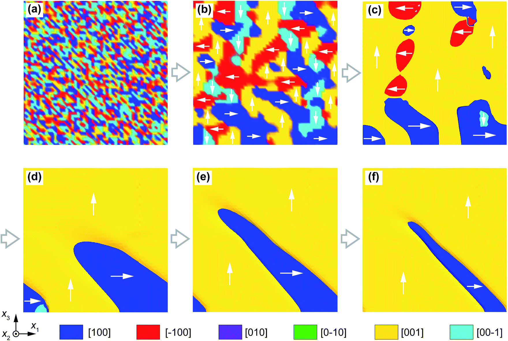
Typical snapshots of temporal polarization distributions in the cgFE thin film at different normalized evolution time are illustrated in Fig. 2. At the beginning of the polarization evolution, a random distribution of polarization is assigned as an initial state (Fig. 2a). Then, polarizations in some local regions gradually align each other to form local rectilinear domains (Fig. 2b), which energetically favour four crystallographic orientations in the x1x3 plane. The formed domains mutually compete, in which some domains expand their sizes while the others shrink and then disappear, i.e., coarsening domain process (Fig. 2c). Specifically, at t* = 6.0, the c-domains cover a large portion of the domain structure in the cgFE thin film, while the a-domains become small and mostly cluster near the bottom surface (Fig. 2c). The c-domain continually expands during the evolution, while the a-domains merge into a single domain, then shrink (Fig. 2d). At the end of evolution, the cgFE thin film exhibits a c/a/c/a-like domain structure with an exclusively needle-like a-domain that terminates in the middle of the film. The system then achieves the equilibrium state. The averaged width of the needle-like domain at the stable state is as small as 10 nm. Compared with the recent experimental report,24 the needle-like domain structure obtained from our developed phase field model achieves highly consistent characteristics, which clearly demonstrates the reliability of the proposed approach.
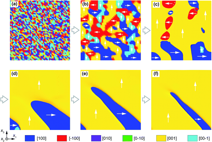 |
| | Fig. 2 Formation of the domain structure in the cgFE PbZr0.8Ti0.2O3 (top) ⇔ PbZr0.2Ti0.8O3 (bottom) thin film. Snapshots of temporal polarization distributions at different evolution times: (a) t* = 0.0, (b) t* = 2.0, (c) t* = 6.0, (d) t* = 10.0, (e) t* = 15.0, and (f) t* = 20.0. | |
In homogeneous ferroelectric thin films, a-domains generally cross through the thickness of the film and form nearly charge-neutral 90° domain walls to achieve the most stable domain configuration in a tetragonal ferroelectric structure.57,62 On the other hand, a-domains that do not extend through the thickness are also observed in real samples,63 where defects such as dislocations likely stabilize the partial a-domains.64–66 In such systems, the a-domains adopt a needle-like shape with straight domain walls and tapered needle point.63 However, the polarization map in Fig. 2f indicates that the domain walls are no longer abrupt but curved, particularly near the needle tip. Such curved domain walls are also clearly observed in experiment.24 This suggests a distinguished characteristic of the partial a-domain in the cgFE thin film.
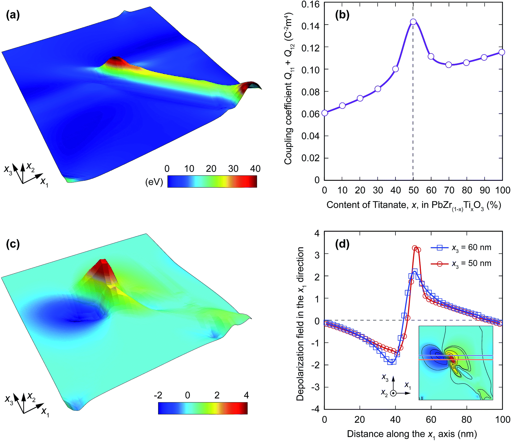
To provide a comprehensive viewpoint on the formation of the needle-like domain and curved domain walls in correlation with the variation of material compositions, we further investigate the distribution of energy densities in the cgFE thin film. Because of the compositional variation, the material properties are spatially dependent in the thickness direction. This bring about the spatial dependence of the polarization magnitude along the thickness, as shown in Fig. S1 in the ESI.† Since both material coefficients and polarization magnitude are dependent of the coordinate in the thickness direction, these significantly effect the distribution of energy densities, particularly the elastic energy density due to polarization-induced strain and the electrostatic energy density due to the internal depolarization field. The distribution of elastic energy density is presented in Fig. 3a. The elastic energy density is large at the a/c domain walls and in the a-domain. In particular, the elastic energy density highly concentrates at the middle of the cgFE thin film. This is because the electrostrictive coefficient (Q11 + Q12) achieves a highest value at the middle of the cgFE PbZr0.8Ti0.2O3 ⇔ PbZr0.2Ti0.8O3 thin film, where the Ti content x is 0.5 in the PbZr(1−x)TixO3 ferroelectric, as shown in Fig. 3b. Such a high concentration of elastic energy further enhances interaction between mechanical and electric fields through the electrostrictive coupling. Since the interaction between mechanical and electric fields is inhomogeneous and particularly high at the middle of the cgFE thin film, the domain wall near the needle-tip departs from the regular a/c domain wall, and thereby, is curved. On the other hand, the inhomogeneous distribution in elastic energy brings about an inhomogeneous distribution in depolarization field through the non-linear electromechanical coupling. As shown in Fig. 3c, the depolarization field in the x1 direction achieves the highest and lowest fields also near the departed domain wall. Interestingly, the highest and lowest values of the depolarization field are at different altitudes from the bottom surface, which originates from the departed domain wall near the needle-tip, as clearly illustrated in Fig. 3d. The high magnitude of the depolarization field, in turn, causes a shrinkage in the size of the a-domain at the middle of the cgFE thin film and a termination of the a-domain within the film. Therefore, the high concentration of elastic energy at the middle of the thin film gives rise to a deflection of the domain wall from the regular a/c domain wall in the cgFE, while the high concentration of depolarization filed shrinks the a-domain near the needle-tip and terminates the a-domain within the cgFE thin film. These originate from the material variation along the thickness of cgFE thin film that brings about a domain structure distinguished from that in homogeneous ferroelectric thin films.
 |
| | Fig. 3 (a) Elastic energy landscape. (b) Dependence of the electrostrictive coefficient on the content of Ti in PbZr(1−x)TixO3. (c) Depolarization field landscape. (d) Distribution of depolarization field along the x1 direction at x3 = 50 nm and x3 = 60 nm, where the depolarization field achieves maximum and minimum values, respectively. | |
3.2 Ferroelastic switching of domain structure in the cgFE thin film under electric/mechanical fields
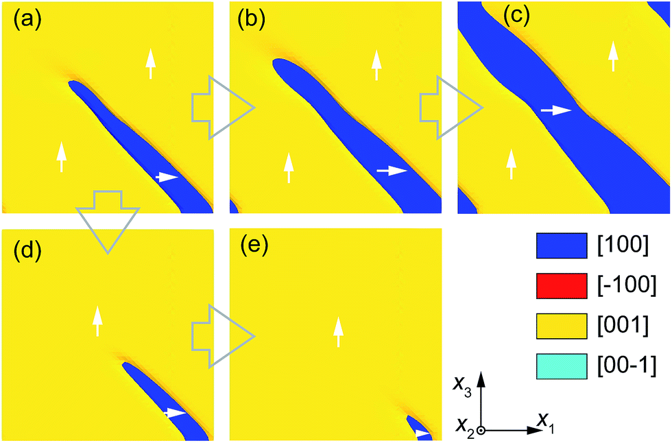
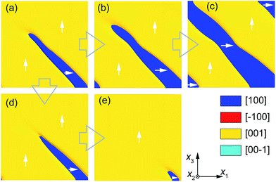
Because of the termination of polarization head-to-tail arrangement, the needle-tip of the a-domain is charged and relatively high in energy, as discussed above. This configuration makes the partial a-domain effectively switchable. To investigate behaviours of the needle-like domain, a small homogeneous electric field is applied along the thickness direction. As a negative electric field is imposed to the cgFE thin film, the upward polar vectors in the c-domain are unfavourable to the applied field. The polar vectors at the needle-tip, where the barrier to polarization rotation is lowest, start to rotate 90° to coincide with the orientation of polar vectors in the a-domain. The switching of polarization under a negative electric field thus simultaneously enlarges and elongates the a-domain, as shown in Fig. 4b. At E = −150 kV cm−1, the needle-tip reaches the top surface of the cgFE thin film, and the domain structure achieves a stripe pattern, where all polarization vectors are in the head-to-tail arrangement, as presented in Fig. 4c. In contrast to the stripe domain structure with straight domain walls in homogeneous ferroelectric thin films, the domain configuration in the cgFE thin film is composed of curved domain walls. On the other hand, as a positive electric field is applied to the cgFE thin film along the thickness direction, the partial a-domain becomes shorter as the polar vectors rotate 90° to coincide with the electric field. The switching also begins from the needle-tip. With an increasing electric field, the partial a-domain gradually shrinks along the long axis (Fig. 4d). However, the partial a-domain still remains, even up to 500 kV cm−1 (Fig. 4e). The needle-like domain, therefore, can be seen to be ferroelastic switchable between several metastable states under an electric field, including partial domains, stripe domains, or nearly single c-domain.
 |
| | Fig. 4 Partial ferroelastic domain switching by electric fields: (a) E = 0.0 (kV cm−1), (b) E = −100 (kV cm−1), (c) E = −150 (kV cm−1), (d) E = 350 (kV cm−1) and (e) E = 500 (kV cm−1). | |
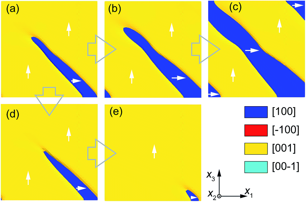
We then investigate the response of the needle-like domain subjected to a mechanical strain along the thickness direction, as shown in Fig. 5. Under compression, the upward polar vectors in the c-domain are unfavourable. The polar vectors at the needle-tip start to rotate 90° to coincide with the orientation of polar vectors in the a-domain. The ferroelastic switching under compression enlarges the a-domain, as shown in Fig. 5b. At ε33 = −2.2%, the needle-tip reaches the top surface of the cgFE thin film, and the domain structure achieves a stripe pattern, as presented in Fig. 5c. Similar to the case with the negative electric field, the stripe domain configuration in the cgFE thin film under compression is composed of curved domain walls. In contrast, under tension, the partial a-domain becomes shorter as the polar vectors rotate 90° to coincide with the applied strain direction. Ferroelastic switching also initiates from the needle tip. With increasing tension, the partial a-domain gradually shrinks along the long axis (Fig. 5d and e). The needle-like domain, thus, can also be switchable between several metastable states under a mechanical field.
 |
| | Fig. 5 Partial ferroelastic domain switching by mechanical fields: (a) ε33 = 0.0, (b) ε33 = −0.004, (c) ε33 = −0.022, (d) ε33 = 0.01 and (e) ε33 = 0.03. | |
3.3 Ferroelectric switching of domain structure in the cgFE thin film: a role of flexoelectricity
To explore how the variation in partial a-domain influences the material and domain wall responses, we consider the ferroelectric switching of the cgFE thin film under a time-dependent sinusoidal electric field as E = Emaxsin(2πft). The electric field is imposed along the thickness direction of the cgFE thin film. From preliminary simulation, the amplitude of the applied field, Emax, is selected equal to 350 kV cm−1 to guarantee for the ferroelectric switching, and the loading frequency is about 0.1 kHz. Note that the macroscopic hysteresis loop of the cgFE thin film observed in experiment is voltage asymmetric, implying that there is preference for the up- or down-poled states. Previous studies have suggested that the primary energy responsible for the asymmetry is electrostatic energy, however, the underlying mechanism for the asymmetry is still unknown. Since the cgFE thin film intrinsically possesses a steep gradient in polarization and strain magnitudes23 (see Fig. S1 in the ESI†), we anticipate that the voltage offset or built-in potential results from the presence of the strain and polarization gradient through the flexoelectric effects. To make this point clear, we investigate the influence of the flexoelectric effect on the ferroelectric switching in the cgFE thin film.
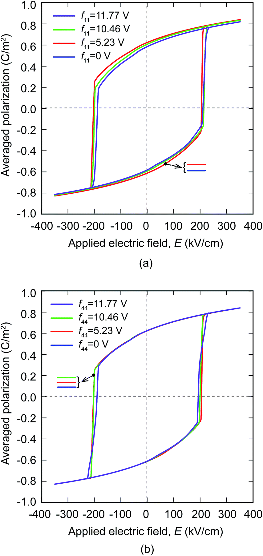
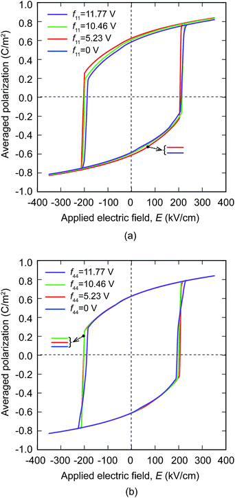
We first investigate the influence of f11 and f44 on the polarization response of the cgFE thin film under external electric loading. Two flexocoupling types (f11 ≠ 0, f12 = 0, f44 = 0) and (f11 = 0, f12 = 0, f44 ≠ 0) are separately investigated for the effects of f11 and f44, respectively. The values of f11 and f44 to be considered here vary from 0 V to 11.77 V.67 The hysteresis loops obtained from different f11 and f44 are presented in Fig. 6a and b, respectively. The macroscopic hysteresis loop exhibits a rectangular-like shape in the absence of the flexoelectric effect (f11 = f12 = f44 = 0), in which the coercive electric field is of about 200 kV cm−1. However, the hysteresis loop slightly shifts towards the positive side of the electric field with the increase in f11 and f44 values, even at a value as large as 11.77 V. This demonstrates that both the f11 and f44 coefficients slightly affect the ferroelectric switching in the cgFE thin film.
 |
| | Fig. 6 Electrical hysteresis loops for: f11 = 0 V, 7.58 V, 10.46 V, and 11.77 V under E = 350 sin(2πft) (kV cm−1). | |
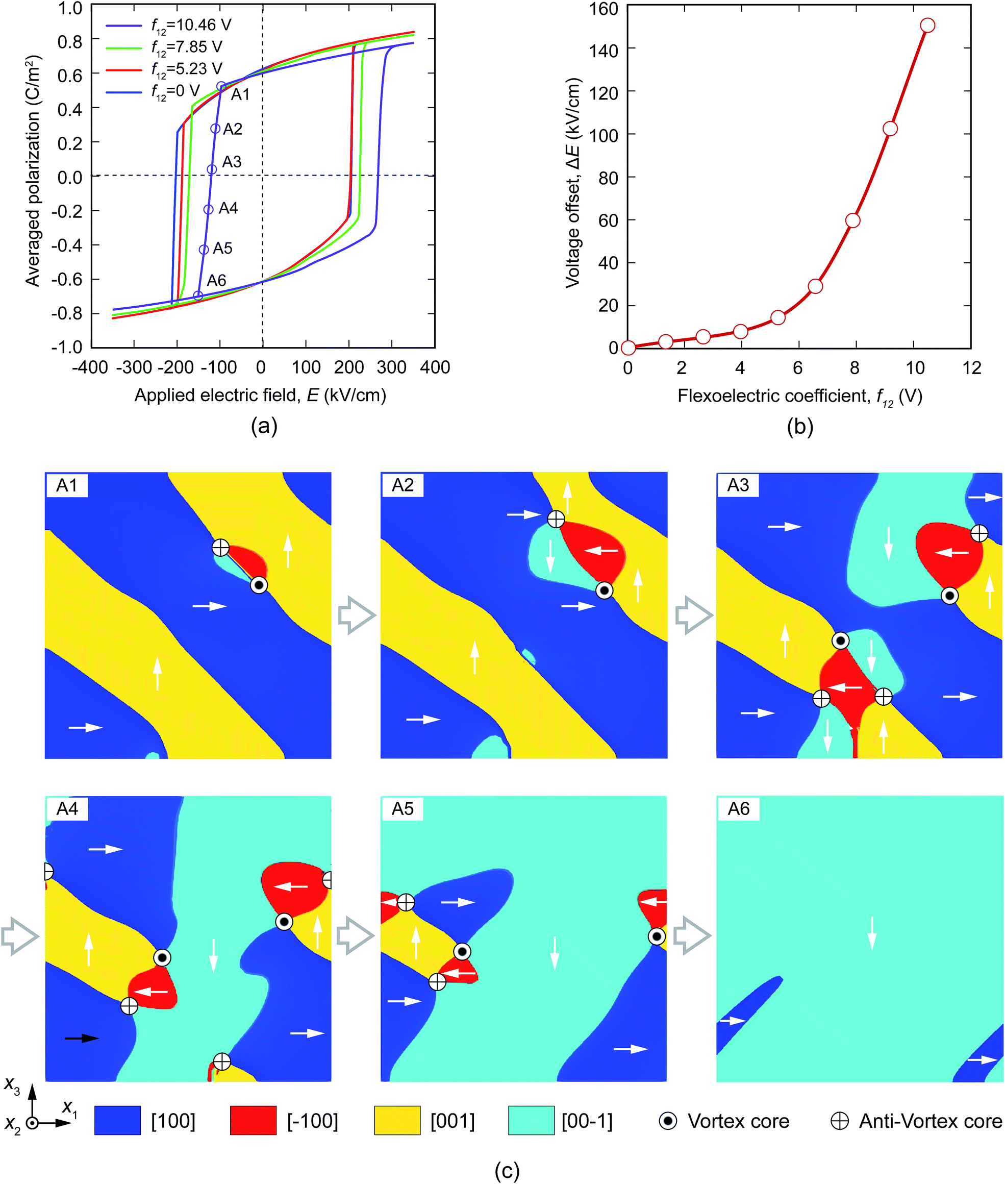
In a similar manner, we continue to investigate the influence of the f12 coefficient on the polarization response of the cgFE thin film under an external electric loading. In this consideration, f11 and f44 are set to be zero, while f12 is considered in a range from 0 V to 10.46 V.67 The hysteresis loop gradually shifts towards the positive side of the electric field as the value of f12 increases from 0 to 7.85 V. The shift becomes significant when f12 is about 10.46 V. Such a voltage offset in the hysteresis loop clearly demonstrates the effect of flexoelectricity on the ferroelectric switching in the cgFE thin film, and is consistent with the observation in the previous experiment.24 On the other hand, the flexoelectric coefficient f12 in the homogeneous PZT is evaluated up to 25 V,48,68 while that in the pure PbTiO3 is about 5 V.48,69 Since flexoelectricity is proportional to permittivity,70–73 the high value of f12 of about 10/12 V for the PbZr0.8Ti0.2O3 ⇔ PbZr0.2Ti0.8O3 thin film, which is roughly as large as the averaged value of the pure PbTiO3 and PZT, is reasonably used in the present study. We further plot in Fig. 7b the dependent profile of the voltage offset, which is characterized by the difference between the coercive electric fields in the positive (EPC) and negative (ENC) electric sides of the hysteresis loop, e.g., ΔE = |EPC| − |ENC|, on the flexoelectric coefficient f12. As f12 is small (f12 ≤ 6 V), ΔE slightly increases with a rise in f12. However, ΔE increases significantly as f12 further increases. This, on the other hand, verifies the unusual and complex evolution of built-in potential in cgFE thin films reported in the previous study.18
 |
| | Fig. 7 (a) Electrical hysteresis loops for: f12 = 0 V, 5.23 V, 7.58 V, and 10.46 V under E = 350 sin(2πft) (kV cm−1). (b) The dependence of voltage offset on the flexoelectric coefficient f12. (c) Snapshots of the polarization structures during the temporal evolution of polarization switching under the coercive electric field, from A1 to A6 for the case of f12 = 10.46 V. | |
On the other hand, to clarify the behaviour of polarization vectors during the switching in the presence of flexoelectricity, typical snapshots of polarization domain structures are presented in Fig. 7c that correspond to points A1–A6 in Fig. 7a for the case of (f12 = 10.46 V, f11 = f44 = 0). At the beginning of the switching (point A1), the polarizations change their orientations at a small local area near the curved domain wall. Such a local change in polarization field originates from an inhomogeneous distribution of electrostatic energy along the curved domain walls. The local change in polarization field interestingly brings about the formation of a local vortex–antivortex pair74,75 within the a/c/a/c-domain structures. As time passes, the vortex and antivortex increase in size, while the vortex and antivortex cores repel each other, as shown at point A2. At point A3, there are several vortex–antivortex pairs formed in the domain structure at the original domain walls. The stripe domain structure is thus almost faded away, and the domain structure with multiple vortices and antivortices emerges. Note that the polarization domains with polarization vector along the electric field are also formed with the formation of vortex and antivortex. Such domains gradually increase in size during the evolution (point A4), then cover a large portion of domain structures (point A5). Simultaneously, vortices and antivortices are forced to shrink. Continuous distortions of polarization can bring vortices and antivortices together and cause them to annihilate. At the end of evolution, new needle-like domains emerge, and the polarization orientation of the c-domain is switched towards the direction of the applied electric field, as shown by point A6. It is noted that a reversed switching phenomenon can occur in a similar manner when the electric field is applied in the opposite direction, yet at a larger coercive field.
To provide a comprehensive viewpoint on the characteristic of polarization switching in the cgFE thin film, we further investigate the switching in a homogeneous PbTiO3 ferroelectric thin film with the same dimensions and simulation set-ups. The obtained results are provided in Fig. S2 within the ESI.† A careful consideration of polarization evolution during the switching suggests that there is no vortex or antivortex formed during the switching since the switching initiates homogeneously from the 90° straight domain walls. At the end of the switching, reversed stripe domains with straight domain walls are obtained. Details of the polarization stripe domain switching are also provided in a previous study.57 Therefore, in the cgFE thin film, the polarization switching process exhibits vastly different responses in comparison to that in the homogeneous ferroelectric thin film. The local switching initiation and the formation and annihilation of vortex–antivortex pairs are unusual phenomena that characterize the ferroelectric switching in the cgFE thin film.
4 Conclusion
In the present study, a new phase field model is developed for cgFE thin films made of PbZr(1−x)TixO3 based on the Ginzburg–Landau theory. The developed approach is validated by comparing the simulation results with several key phenomena occurring in cgFE thin films that are observed from experiment, such as the formation of needle-like domains with curved domain walls and the voltage offset of the hysteresis loop. We demonstrate that the high concentration of elastic energy near the needle-tip of the a-domain gives rise to a deflection of the domain wall from the regular a/c domain wall in the cgFE thin film, while the high concentration of the depolarization field shrinks the a-domain near the needle-tip and terminates the domain within the thin film. As a result, such a high concentration of elastic energy and depolarization field facilitates the stabilization of needle-like domains with curved domain walls in the cgFE thin film. The needle-like domain can be extended upwards to the surface of the film through ferroelastic switching under the application of electric field or compression at the surface of the film. Our results also show that the ferroelastic switching initiates at the high-energy point of the needle, where the polarization rotation is initiated. Furthermore, flexoelectricity is proven to play an important role in the voltage offset of the hysteresis loop. On the other hand, the ferroelectric switching process in the cgFE thin film exhibits vastly different responses in comparison to that in homogeneous ferroelectric thin films, including local switching initiation, and the formation and annihilation of vortex–antivortex pairs during the switching. The present study, therefore, provides an incisive approach for an increasingly important class of materials formed by cgFEs, which may bring new understanding and unique insights of these complex cgFE materials, as well as novel potential applications.
Conflicts of interest
There are no conflicts to declare.
Acknowledgements
This research is funded by the Vietnam National Foundation for Science and Technology Development (NAFOSTED) under grant number 103.02-2018.06.
Notes and references
- J. F. Scott and C. A. P. De Araujo, Science, 1989, 246, 1400–1405 CrossRef CAS PubMed.
- J. Scott, Science, 2007, 315, 954–959 CrossRef CAS PubMed.
- S. Miller and P. McWhorter, J. Appl. Phys., 1992, 72, 5999–6010 CrossRef CAS.
- S. Mathews, R. Ramesh, T. Venkatesan and J. Benedetto, Science, 1997, 276, 238–240 CrossRef CAS PubMed.
- E. Y. Tsymbal and H. Kohlstedt, Science, 2006, 313, 181–183 CrossRef CAS PubMed.
- W. Eerenstein, N. Mathur and J. F. Scott, Nature, 2006, 442, 759 CrossRef CAS PubMed.
- L. V. Lich, T. Shimada, K. Miyata, K. Nagano, J. Wang and T. Kitamura, Appl. Phys. Lett., 2015, 107, 232904 CrossRef.
- T. Choi, S. Lee, Y. Choi, V. Kiryukhin and S.-W. Cheong, Science, 2009, 324, 63–66 CrossRef CAS PubMed.
- M. Brazier, M. McElfresh and S. Mansour, Appl. Phys. Lett., 1999, 74, 299–301 CrossRef CAS.
- N. W. Schubring, J. V. Mantese, A. L. Micheli, A. B. Catalan and R. J. Lopez, Phys. Rev. Lett., 1992, 68, 1778 CrossRef CAS PubMed.
- J. V. Mantese, N. W. Schubring, A. L. Micheli, A. B. Catalan, M. S. Mohammed, R. Naik and G. W. Auner, Appl. Phys. Lett., 1997, 71, 2047–2049 CrossRef CAS.
- M. Brazier, M. McElfresh and S. Mansour, Appl. Phys. Lett., 1998, 72, 1121–1123 CrossRef CAS.
- D. Bao, X. Yao and L. Zhang, Appl. Phys. Lett., 2000, 76, 2779–2781 CrossRef CAS.
- N. Choudhury, L. Walizer, S. Lisenkov and L. Bellaiche, Nature, 2011, 470, 513 CrossRef CAS PubMed.
- S. Ezhilvalavan and T.-Y. Tseng, Mater. Chem. Phys., 2000, 65, 227–248 CrossRef CAS.
- S. Zhong, S. Alpay, Z.-G. Ban and J. Mantese, Appl. Phys. Lett., 2005, 86, 092903 CrossRef.
- G. Akcay, S. Zhong, B. Allimi, S. Alpay and J. Mantese, Appl. Phys. Lett., 2007, 91, 012904 CrossRef.
- J. C. Agar, A. R. Damodaran, G. A. Velarde, S. Pandya, R. Mangalam and L. W. Martin, ACS Nano, 2015, 9, 7332–7342 CrossRef CAS PubMed.
- X. Zhu, N. Chong, H. L.-W. Chan, C.-L. Choy, K.-H. Wong, Z. Liu and N. Ming, Appl. Phys. Lett., 2002, 80, 3376–3378 CrossRef CAS.
- X. Zhu, J. Zhu, S. Zhou, Z. Liu, N. Ming, H. L.-W. Chan, C.-L. Choy, K.-H. Wong and D. Hesse, Mater. Sci. Eng., B, 2005, 118, 219–224 CrossRef.
- D. Maurya, F.-C. Sun, S. P. Alpay and S. Priya, Sci. Rep., 2015, 5, 15144 CrossRef CAS PubMed.
- R. Mangalam, J. Karthik, A. R. Damodaran, J. C. Agar and L. W. Martin, Adv. Mater., 2013, 25, 1761–1767 CrossRef CAS PubMed.
- A. R. Damodaran, S. Pandya, Y. Qi, S.-L. Hsu, S. Liu, C. Nelson, A. Dasgupta, P. Ercius, C. Ophus and L. R. Dedon, et al., Nat. Commun., 2017, 8, 14961 CrossRef PubMed.
- J. Agar, A. Damodaran, M. Okatan, J. Kacher, C. Gammer, R. Vasudevan, S. Pandya, L. Dedon, R. Mangalam and G. Velarde, et al., Nat. Mater., 2016, 15, 549 CrossRef CAS PubMed.
- X. Wang, C. Wang, W. Zhong and P. Zhang, Phys. Lett. A, 2001, 285, 212–216 CrossRef CAS.
- H.-X. Cao and Z.-Y. Li, J. Phys.: Condens. Matter, 2003, 15, 6301 CrossRef CAS.
- J. Karthik, R. V. K. Mangalam, J. C. Agar and L. W. Martin, Phys. Rev. B, 2013, 87, 024111 CrossRef.
- J. Zhang, R. Xu, A. R. Damodaran, Z.-H. Chen and L. W. Martin, Phys. Rev. B, 2014, 89, 224101 CrossRef.
- I. Misirlioglu and S. Alpay, Acta Mater., 2017, 122, 266–276 CrossRef CAS.
- Y. Qiu, H. Wu, J. Wang, J. Lou, Z. Zhang, A. Liu and G. Chai, J. Appl. Phys., 2018, 123, 084103 CrossRef.
- H.-L. Hu and L.-Q. Chen, J. Am. Ceram. Soc., 1998, 81, 492–500 CrossRef CAS.
- Y. Li, S. Hu, Z. Liu and L. Chen, Appl. Phys. Lett., 2001, 78, 3878–3880 CrossRef CAS.
- S. Hu and L. Chen, Acta Mater., 2001, 49, 1879–1890 CrossRef CAS.
- L.-Q. Chen, Annu. Rev. Mater. Res., 2002, 32, 113–140 CrossRef CAS.
- L. V. Lich, T. Shimada, K. Nagano, Y. Hongjun, J. Wang, K. Huang and T. Kitamura, Acta Mater., 2015, 88, 147–155 CrossRef CAS.
- L. V. Lich, T. Shimada, S. Sepideh, J. Wang and T. Kitamura, Acta Mater., 2017, 125, 202–209 CrossRef.
- L. V. Lich, T. Shimada, J. Wang, V.-H. Dinh, T. Q. Bui and T. Kitamura, Phys. Rev. B, 2017, 96, 134119 CrossRef.
- G. Shirane, R. Pepinsky and B. C. Frazer, Acta Crystallogr., 1956, 9, 131–140 CrossRef CAS.
- J. Wang, S.-Q. Shi, L.-Q. Chen, Y. Li and T.-Y. Zhang, Acta Mater., 2004, 52, 749–764 CrossRef CAS.
- M. J. Haun, E. Furman, S. Jang, H. McKinstry and L. Cross, J. Appl. Phys., 1987, 62, 3331–3338 CrossRef CAS.
- M. J. Haun, E. Furman, S. J. Jang and L. E. Cross, Ferroelectrics, 1989, 99, 13–25 CrossRef CAS.
- S. Choudhury, Y. Li and L.-Q. Chen, J. Am. Ceram. Soc., 2005, 88, 1669–1672 CrossRef CAS.
- Y. Li, S. Hu and L. Chen, J. Appl. Phys., 2005, 97, 034112 CrossRef.
- M. J. Haun, E. Furman, H. A. McKinstry and L. E. Cross, Ferroelectrics, 1989, 99, 27–44 CrossRef CAS.
- M. J. Haun, Z. Q. Zhuang, E. Furman, S. J. Jang and L. E. Cross, Ferroelectrics, 1989, 99, 45–54 CrossRef CAS.
- W. Cao and L. E. Cross, Phys. Rev. B, 1991, 44, 5 CrossRef.
- N. Pertsev, V. Kukhar, H. Kohlstedt and R. Waser, Phys. Rev. B, 2003, 67, 054107 CrossRef.
- P. Zubko, G. Catalan and A. K. Tagantsev, Annu. Rev. Mater. Res., 2013, 43, 387–421 CrossRef CAS.
- P. Yudin and A. Tagantsev, Nanotechnology, 2013, 24, 432001 CrossRef CAS PubMed.
- Q. Li, C. Nelson, S.-L. Hsu, A. Damodaran, L.-L. Li, A. Yadav, M. McCarter, L. Martin, R. Ramesh and S. Kalinin, Nat. Commun., 2017, 8, 1468 CrossRef CAS PubMed.
- Y. Cao, A. Morozovska and S. V. Kalinin, Phys. Rev. B, 2017, 96, 184109 CrossRef.
- J. Wang, Y. Li, L.-Q. Chen and T.-Y. Zhang, Acta Mater., 2005, 53, 2495–2507 CrossRef CAS.
- R. D. Mindlin, Int. J. Solids Struct., 1965, 1, 417–438 CrossRef.
- Y. L. Li, S. Y. Hu, Z. K. Liu and L. Q. Chen, Acta Mater., 2002, 50, 395–411 CrossRef CAS.
- P. Song, T. Yang, Y. Ji, Z. Wang, Z. Yang, L. Chen and L. Chen, Comput. Phys. Commun., 2017, 21, 1325–1349 CrossRef.
- W. Shu, J. Wang and T.-Y. Zhang, J. Appl. Phys., 2012, 112, 064108 CrossRef.
- L. V. Lich, T. Shimada, J. Wang and T. Kitamura, Acta Mater., 2016, 112, 1–10 CrossRef CAS.
- M. J. Haun, E. Furman, T. R. Halemane and L. E. Cross, Ferroelectrics, 1989, 99, 55–62 CrossRef CAS.
- M. J. Haun, E. Furman, S. J. Jang and L. E. Cross, Ferroelectrics, 1989, 99, 63–86 CrossRef CAS.
- P. Gao, J. Britson, J. R. Jokisaari, C. T. Nelson, S.-H. Baek, Y. Wang, C.-B. Eom, L.-Q. Chen and X. Pan, Nat. Commun., 2013, 4, 2791 CrossRef.
- F. Xue, J. J. Wang, G. Sheng, E. Huang, Y. Cao, H. H. Huang, P. Munroe, R. Mahjoub, Y. L. Li and V. Nagarajan, et al., Acta Mater., 2013, 61, 2909–2918 CrossRef CAS.
- B. Meyer and D. Vanderbilt, Phys. Rev. B, 2002, 65, 104111 CrossRef.
- P. Gao, J. Britson, C. T. Nelson, J. R. Jokisaari, C. Duan, M. Trassin, S.-H. Baek, H. Guo, L. Li and Y. Wang, et al., Nat. Commun., 2014, 5, 3801 CrossRef CAS PubMed.
- D. Su, Q. Meng, C. Vaz, M.-G. Han, Y. Segal, F. J. Walker, M. Sawicki, C. Broadbridge and C. H. Ahn, Appl. Phys. Lett., 2011, 99, 102902 CrossRef.
- M.-W. Chu, I. Szafraniak, R. Scholz, C. Harnagea, D. Hesse, M. Alexe and U. Gösele, Nat. Mater., 2004, 3, 87 CrossRef CAS PubMed.
- T. Kiguchi, K. Aoyagi, Y. Ehara, H. Funakubo, T. Yamada, N. Usami and T. J. Konno, Sci. Technol. Adv. Mater., 2011, 12, 034413 CrossRef PubMed.
- P. Yudin, R. Ahluwalia and A. Tagantsev, Appl. Phys. Lett., 2014, 104, 082913 CrossRef.
- W. Ma and L. E. Cross, Appl. Phys. Lett., 2003, 82, 3293–3295 CrossRef CAS.
- G. Catalan, A. Lubk, A. Vlooswijk, E. Snoeck, C. Magen, A. Janssens, G. Rispens, G. Rijnders, D. Blank and B. Noheda, Nat. Mater., 2011, 10, 963 CrossRef CAS PubMed.
- S. M. Kogan, Soviet Physics - Solid State, 1964, 5, 2069–2070 Search PubMed.
- G. Catalan, L. Sinnamon and J. Gregg, J. Phys.: Condens. Matter, 2004, 16, 2253 CrossRef CAS.
- L. E. Cross, J. Mater. Sci., 2006, 41, 53–63 CrossRef CAS.
- P. Zubko, G. Catalan, A. Buckley, P. R. L. Welche and J. F. Scott, Phys. Rev. Lett., 2007, 99, 167601 CrossRef CAS PubMed.
- I. I. Naumov, L. Bellaiche and H. Fu, Nature, 2004, 432, 737–740 CrossRef CAS PubMed.
- L. V. Lich, T. Shimada, J. Wang and T. Kitamura, Nanoscale, 2017, 9, 15525–15533 RSC.
Footnote |
| † Electronic supplementary information (ESI) available: Supplement figures; brief description of the polarization switching in homogeneous ferroelectric under electric field. See DOI: 10.1039/c8ra10614b |
|
| This journal is © The Royal Society of Chemistry 2019 |
Click here to see how this site uses Cookies. View our privacy policy here. 
 Open Access Article
 This Open Access Article is licensed under a Creative Commons Attribution-Non Commercial 3.0 Unported Licence
 * and
Van-Hai Dinh
* and
Van-Hai Dinh