
 Open Access Article
 This Open Access Article is licensed under a Creative Commons Attribution-Non Commercial 3.0 Unported Licence
Photocatalytic properties of a new Z-scheme system BaTiO3/In2S3 with a core–shell structure
Kaili Weia,
Baolai Wanga,
Jiamin Hu a,
Fuming Chena,
Qing Haob,
Guannan Hea,
Yinzhen Wanga,
Wei Lia,
Junming Liua and
Qinyu He*a
a,
Fuming Chena,
Qing Haob,
Guannan Hea,
Yinzhen Wanga,
Wei Lia,
Junming Liua and
Qinyu He*a
aSouth China Normal University, China
bUniversity of Arizona, USA
First published on 11th April 2019
Abstract
It's highly desired to design and fabricate an effective Z-scheme photo-catalyst with excellent charge transfer and separation, and a more negative conduction band edge (ECB) than O2/·O2− (−0.33 eV) and a more positive valence band edge (EVB) than ·OH/OH− (+2.27 eV) which provides high-energy redox radicals. Herein, we firstly designed and synthesized a core–shell-heterojunction-structured Z-scheme system BaTiO3@In2S3 (BT@IS, labelled as BTIS) through a hydrothermal method, where commercial BT was used as the core and In(NO3)3·xH2O together with thioacetamide as the precursor of IS was utilized as the shell material. In this system, the shell IS possesses a ECB of −0.76 eV and visible-light-response Eg of 1.92 eV, while the core BT possesses a EVB of 3.38 eV, which is well suited for a Z-scheme. It was found that the as-prepared BTIS possesses a higher photocatalytic degradation ability for methyl orange (MO) than commercial BT and the as-prepared IS fabricated by the same processing parameters as those of BTIS. Holes (h+) and superoxide radicals (·O2−) were found to be the dominant active species for BTIS. In this work, the core–shell structure has inhibited the production of ·OH because the shell IS has shielded the OH− from h+. It is assumed that if the structure of BTIS is a composite, not a core–shell structure, ·OH could be produced during photocatalysis, and therefore a higher photocatalytic efficiency would be obtained. This current work opens a new pathway for designing Z-scheme photocatalysts and offers new insight into the Z-scheme mechanism for applications in the field of photocatalysis.
1. Introduction
With the growth of worldwide industry, serious environmental contamination has become a major concern of our society. Semiconductor based photocatalysis is considered to be an effective route to address the environmental pollution issues.1,2 In the past several decades, various metal oxide semiconductors, such as TiO2, ZnO, SnO2, and Bi-based oxides have been proven to be effective photo-catalysts under UV-light.3–6 However, UV-light accounts for only about 4% of sunlight. In order to utilize more sunlight, considerable efforts, mainly including introduction of dopants and oxygen deficiencies,7–9 and constructing heterojunctions,10 have been made to narrow their band energy gaps (Eg) and broaden their absorption light spectrum to visible light which accounts for about 43% of sunlight.11–15 But the narrow-Eg semiconductors and dopants bring about a new problem.16,17 Their photogenerated electrons and holes recombine more easily than those in wide Eg semiconductors.To this end, many strategies have been investigated to promote the charge separation, such as surface modification of photocatalysts with co-catalysts,18 artificially constructing heterojunctions and Z-scheme systems,19–21 and introducing an electron capturing level in the band gap that would generate some defects in the metal oxide lattice and help to capture charge carriers,22 or employing perovskites with an intrinsic electric dipole moment which can separate photo-induced electrons and holes,23 or utilizing semiconductors with long lifetime of the excited triplet states.24,25 Among the above-mentioned strategies, Z-scheme mechanism is the most effective strategy to improve the photogenerated carrier separation ability.26,27
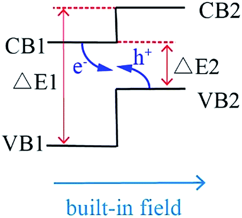
The mechanism of Z-scheme is schematically demonstrated in Scheme 1. The position of valence band (VB) and conduction band (CB) of semiconductor 2 is higher than that of semiconductor 1, and the steps in the CB-s and VB-s go in the same direction. There are two excellent advantages in Z-scheme system. First, the difference of chemical potential between semiconductor 1 and 2 causes band bending at the interface of junction. The band bending induces a built-in field, which drives the photogenerated electrons and holes to move in opposite directions, leading to a spatial separation of the electrons and holes on different sides of heterojunction. Thus, the formation of heterostructures like shown in Scheme 1 is an effective approach to enhance charge separation efficiency for improved photocatalytic degradation activity. Second, under light irradiation, the electrons in VB of semiconductor 1 (VB1) and semiconductor 2 (VB2) would jumps to their CB bottoms. Because the CB of semiconductor 1 (CB1) is closer to VB2, the photogenerated electrons in CB1 is easier to recombine with the holes in VB2. Therefore, the left electrons in conduction band of semiconductor 2 (CB2) possesses more negative potential than the redox potential of O2/·O2− (−0.33 eV)28 and holes in VB1 possess more positive potential than ·OH/OH− (+2.27 eV),29 resulting in that the organic pollutants would degrade completely without intermediates even though the semiconductor 1 and semiconductor 2 are narrow-Eg semiconductors.
 | ||
| Scheme 1 Schematic representation of Z-scheme system. | ||
Based on the mechanism of Z-scheme, it is assumed that there are two main factors to be considered when selecting the semiconductors for Z-scheme system: firstly, the potential of CB2 and VB1 should be more negative than the redox potential of O2/·O2− (−0.33 eV)28 and VB1 should be more positive than ·OH/OH− (+2.27 eV).29 And secondly, the ΔE2 value in Scheme 1 should be as small as possible and ΔE1 value in Scheme 1 should be as large as possible. To date, a large number of Z-scheme photocatalytic systems have been fabricated and developed to achieve a higher photocatalytic efficiency in comparison with those of the single components under visible light irradiation, such as In2S3/Ag2CrO4,30 In2S3/Ag3PO4,31 CuInS2/g-C3N4,32 2D ZnO/ZnxCd1−xS,33 etc. However, we have noticed that the hybridized semiconductors with heterojunction In2S3 (IS)/BaTiO3 (BT) have not been reported. It was reported that the VB and CB of BT are 3.38 eV and 0.08 eV,34 respectively, while the VB and CB of IS are 1.15 eV and −0.77 eV,30 respectively. If IS and BT construct a heterogeneous Z-scheme system, its CB of −0.77 eV is more negative than the redox potential of O2/·O2− (−0.33 eV) and its VB of 3.38 eV is more positive than ·OH/OH− (+2.27 eV), conforming to the requisites of good Z-scheme system.
On the other hand, it is reported that core–shell structured heterojunctions would favor in prolong the lifetime of photo-generated carriers.1 Therefore, in this work, the heterojunction BT/IS was prepared in a core–shell structure through hydrothermal method (IS as shell). The photocatalytic activities was evaluated by studying the degradation of methyl orange (MO) under UV-visible light irradiation. An enhanced photocatalytic activity was found and ·O2− and h+ was found to be the dominant active species.
2. Experimental
2.1 Preparation of the core–shell structured BaTiO3/In2S3 composite
BTIS was synthesized using a hydrothermal method as follows. 1 mmol of In(NO3)3·xH2O (99.99%, Aladdin Industrial Corporation) and 2.4 mmol of thioacetamide (99.0%, Sinopharm Chemical Reagent Co, Ltd) were dissolved in 80 mL of deionized water with magnetically stirring for 15 min. Then, 0.065 g of commercial BaTiO3 (99.5%, Aladdin Industrial Corporation) was added and continued stirring for 10 min, followed by ultrasonicating for 2 min. Then the mixture was poured into a 100 ml Teflon lined stainless-steel autoclave and maintained at 180 °C for 12 h. Finally, the as-obtained precipitates was washed with distilled water and ethanol alternately and subsequently dried in an oven at 80 °C for 12 h. The as-prepared powder is denoted by BTIS.In order to elucidate the effect of the core–shell structured heterojunction BT/IS on the photocatalytic properties, pure IS was prepared using the identical procedure but without BT added. Simultaneously, the above-said commercial BT was characterized by using identical techniques with BTIS and IS as comparison.
2.2. Characterization
The crystalline structures of BT, IS and BTIS were investigated by X-ray diffraction (XRD) using an X'Celerator detector (XRD, X'Pert Pro, PANalytical, Los Altos, CA) with a slow scanning speed of 1° min−1 and Cu Kα radiation (k = 1.5406 Å) in the 2θ range of 5–80°. A Carl Zeiss 55 instrument (Carl Zeiss Microscopy GmbH, Germany) was used to probe the morphology of IS, BT and BTIS. The detailed microstructures of BTIS was observed by high-resolution transmission electron microscopy (HRTEM, JEM-2100HR, JEOL, Japan). X-ray photoelectron spectroscopy (XPS) measurements were performed to investigate the binding states of indium (In), sulfur (S), barium (Ba), titanium (Ti), and oxygen (O) atoms in above-said three samples using an Thermo Scientific K-Alpha XPS system (Thermo Fisher Scientific, America). UV-vis diffuse reflectance spectrum (UV-vis-DRS) measurements of BT, IS and BTIS were performed by a Shimadzu 2550 PC spectrophotometer, using BaSO4 as a reference sample. A photoluminescence (PL) spectra of BT, IS and BTIS recorded on a Hitachi F-4500 fluorescence spectrophotometer (Hitachi, Japan) were employed to qualitatively characterize the recombination rates of the photogenerated electron–hole pairs. Inductively coupled plasma-atomic emission spectrometry (ICP-AES) measurement was performed by SPECTRO ARCOS.2.3. Photocatalytic tests
The photocatalytic activities of BT, IS and BTIS were examined by degrading MO (AR, Aladdin Industrial Corporation) in a quartz reactor with a water-cooling outer pack (Shanghai Lansheng Company) under a simulated solar light source produced by a 350 W-xenon lamp. These experiments involved two steps. Initially, the dark condition were applied to reveal the adsorption of MO and photocatalyst active material; 50 mg of photocatalysts were plugged into 100 mL of MO solution (10 mg L−1) and stirred in the dark and the MO concentration was monitored and completes when it reaches the adsorption–desorption equilibrium. Secondly, the photocatalytic behavior was carried out under simulated solar light. The MO concentration was monitored as follows; at given time intervals, 1.5 mL of suspension was collected and centrifuged to remove the catalyst. The concentration of MO was measured using UV-vis spectrometry according to the maximum absorption intensity of the peak around 464 nm.35The degradation rate of MO is expressed in eqn (1):
| Degradation rate (%) = (C0 − C)/C0 × 100% = ((A0 − A)/A0) × 100% | (1) |
2.4 Photoelectrochemical experiments
The electrochemical impedance spectroscopy (EIS) measurements were carried out by employing a CHI660E electrochemistry workstation (Shanghai, China) at room temperature. All the experiments were performed in a standard three-electrode cell using the photocatalytic material-deposited fluoride tin oxide (FTO) electrode as the working electrode, a saturated calomel electrode (SCE) as the reference electrode, and a platinum sheet (1 cm2) as the auxiliary electrode. 0.5 mol L−1 Na2SO4 aqueous solution was used as the supporting electrolyte. A 350 W Xe lamp was utilized as the light source. The working electrodes were fabricated according to the described in previous literature.36 FTO glass pieces were rinsined alternatively by using ethyl alcohol and distilled water, and then dried at 50 °C. Then, 0.027 g of the sample and 0.003 g of polyvinylidene fluoride were mixed. After adding 1-methyl-2-pyrrolidinone, the mixture was ultrasonicated to obtain a suspension, which was then coated onto the FTO glass substrate. The coated area on the FTO glass was controlled to 0.8 × 0.8 cm2. Finally, the coated FTO glass was dried at 60 °C to obtain the working electrode.3. Result and discussion
3.1 Phases and microstructures
Fig. 1 shows the XRD patterns (Fig. 1) of IS, BT and BTIS. The XRD patterns of BT and IS agree well with the standard PDF cards 05-0626 (indicated by sign “●”) and 25-0390 (indicated by sign “▽”), respectively. In BTIS, the distinctive peaks at 2θ = 27.2°, 33.2° and 47.9° attributes to the faces (109), (0012) and (2212) of IS, respectively, while the weak peak at 31.5°, 38.7°, 45.4°, 56.2° could be attributed to the faces (101), (111), (200), (211) of BT, respectively. The intensity of pure IS is much lower than that of pure BT. But in BTIS the intensities of BT is, on the contrary, obviously lower than that of IS, indicating the core–shell structured heterojunction BT/IS in BTIS.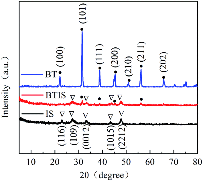 | ||
| Fig. 1 XRD patterns of IS, BT and BTIS. | ||
The scanning electron microscopy (SEM) (Fig. 2a–c) and HRTEM (Fig. 2d) investigations can further confirm the core–shell structured heterojunction BT@IS in BTIS. As shown in Fig. 2a and b, the pristine BT has a mean particle size of around 1 μm, while the prepared pure IS has a mean particle size of around 25 nm. Because the processing parameters of preparing IS and depositing IS on BT are identical, the particle size of IS in BTIS should be close to 25 nm. Fig. 2c shows the core–shell BTIS, consisting of the pristine BT with large particle size around 1 μm and the deposited IS with the small particles size around 25 nm decorated on the BT. However, the IS particles has not completely encapsulated the large BT particle. To further reveal the formation of core–shell structure, HR-TEM images were captured as shown in Fig. 2d and it was found that a core field with lattice spacing of 0.226 nm and shell field with a fringe spacing of 0.323 nm could attribute to the (111) plane of BT (JCPDS no. 05-0626) and the (109) facet of IS (JCPDS no. 25-0390), respectively, suggesting the formed core–shell structured BT@IS in BTIS.
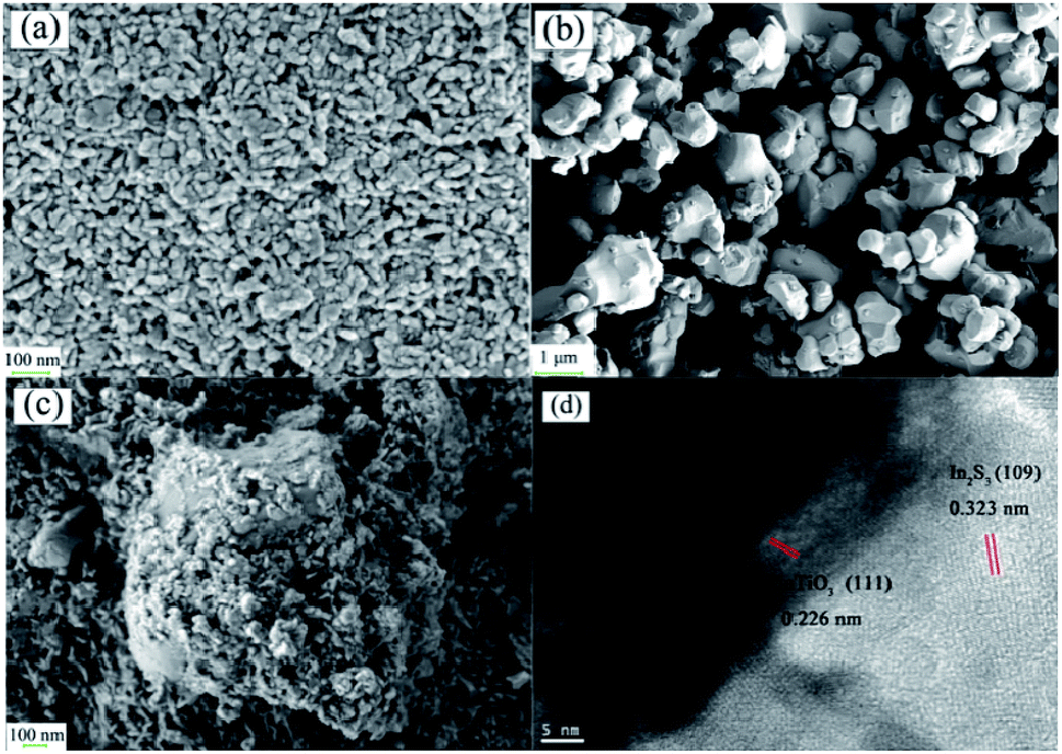 | ||
| Fig. 2 SEM images of (a) IS, (b) pristine BT, (c) BTIS, and HRTEM image of (d) BTIS. | ||
In order to verify the elemental distribution of the BTIS composite structure, the energy-dispersive X-ray spectrometry (EDS) analysis and element mapping was conducted. As presented in Fig. 3a–f, the Ba, Ti, O, In and S elements existed in the composite, and IS was homogeneously distributed on the BT surface, which was consistent with the results of SEM and TEM.
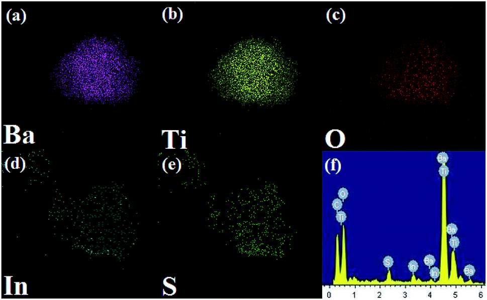 | ||
| Fig. 3 EDS mapping of individual elements in BTIS: (a) Ba, (b) Ti, (c) O, (d) In, (e) S, (f) EDS spectrum of BTIS. | ||
The BET areas and pore size of IS, BTIS and BT have been measured. From Table 1, it can be seen that the calculated BET area of IS was 104.21 m2 g−1, which was much higher than that of BT (1.68 m2 g−1). Meanwhile, because the IS grew on the particle surface of BT, the BET area of BTIS had increased to 72.70 m2 g−1, much larger than that of pure BT.
| Samples | IS | BTIS | BT |
|---|---|---|---|
| BET area (m2 g−1) | 104.21 | 72.70 | 1.68 |
| Pore volume (cm3 g−1) | 0.32 | 0.234 | 0.007 |
| Pore size (nm) | 13.1 | 12.9 | 17.49 |
The specific data of ICP-AES is listed in Table 2. It can be seen that the total mass ratio of In and S elements is 71.99%, which is close to the theoretical mass fraction of In2S3 in BTIS.
| Element | Ba | Ti | In | S |
|---|---|---|---|---|
| Contents (wt%) | 9.96 | 6.78 | 50.73 | 21.26 |
3.2 XPS analysis
Fig. 4a shows the XPS survey spectrum of BTIS. It clearly shows the corresponding peaks of S, In, Ba, Ti and O elements. It can be also seen that the peaks of In 3d and S 2p are stronger, while the peaks of Ba 3d and O 1 s are weaker, suggesting the formation of core–shell structured BT@IS.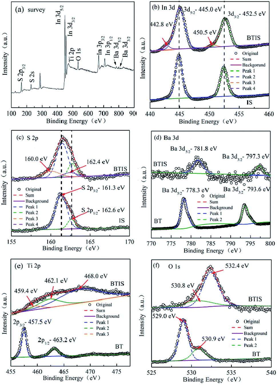 | ||
| Fig. 4 XPS survey spectrum (a) of BTIS, high-resolution XPS spectra of BTIS and IS for (b) In 3d, (c) S 2p, respectively; high-resolution XPS spectra of BTIS and BT for (d) Ba 3d, (e) Ti 2p and (f) O 1s, respectively. | ||
Fig. 4b is the high-resolution XPS spectra of In 3d profiles for BTIS and IS. Two peaks were observed in the spectrum of IS around 444.9 eV and 452.5 eV, ascribed to the In3+ 3d5/2 and In3+ 3d3/2, respectively.37 In BTIS, the exhibited peaks of In3+ 3d5/2 and In3+ 3d3/2 shift to a bit higher values, 445.0 eV and 452.6 eV, respectively. It is reported that built-in electric fields in the heterojunctions WO3/TiO2 and CdSe/CdTe could would result in the shift of binding energy.39,40 Therefore, the shift to higher binding energy for In3+ 3d5/2 and In3+ 3d3/2 could be ascribed to the heterojunction BT@IS.
Fig. 4c is the high-resolution XPS spectra of S 2p for BTIS and IS. In IS, two peaks at 161.3 eV, 162.6 eV were deconvoluted, corresponding to S2+ 2p3/2 and S 2p1/2,40,41 respectively. With respect to BTIS, besides the two peaks at 161.3 eV and 162.6 eV which are respectively attributed to S2+ 2p3/2 and S 2p1/2 in the location far from the heterojunction of BT@IS, there are still two additional peaks at 160.0 eV and 162.4 eV were fitted, also ascribed to S 2p3/2 and S 2p1/2 in the heterojunction of BT@IS,38,39 respectively.
The high-resolution XPS spectra of Ba 3d for BTIS and BT are shown in Fig. 4d. BT exhibits two peaks at 778.3 eV and 793.6 eV, attributing to Ba 3d5/2 and Ba 3d3/2.42,43 Whereas in BTIS, both the peaks of Ba 3d5/2 and Ba 3d3/2 shift to higher values of 781.8 eV and 797.3 eV, respectively, probably resulting from the lattice distortion and internal field in the heterojunction of BT@IS.38,39
The Ti 2p spectra (Fig. 4e) reveals that the pristine BT exhibits two peaks at 457.5 and 463.2 eV, attributing to Ti4+ 2p3/2 and Ti4+ 2p1/2 according to ref. 44–47. In BTIS, there is a big widening block. In previous work, Ren et al. found a similar XPS block of Ti 2p produced by heterojunction Bi2O3/BaTiO3.48 Therefore, the heterojunction BT/IS could account for the XPS block of Ti 2p in BTIS. Considering the presence of the heterojunction BT/IS, three peaks were fitted for this XPS block of BTIS at 459.4 eV, 462.1 eV and 468.0 eV, corresponding to the Ti–S bond, Ti4+ 2p3/2 and Ti4+ 2p1/2, respectively. Comparing with those reported in other refs, the peaks have shift to higher values due to the heterojunction BT@IS.48,49
The high resolution scanning of O 1s spectra for BT and BTIS with the Gaussian function are shown in Fig. 4f. In BT, the Gaussian function with the two splitted peaks at 529.0 eV and 530.9 eV denotes the presence of two different O species. From the above discussion about Ti 2p, it is known that there is no Ti3+ ions. Therefore, the presence of oxygen vacancy should be excluded. The two splitted peaks at 529.0 eV and 530.9 eV should be attributed to lattice oxygen (OL) of bunding Ba–Ti–O bond like in ref. 50 and absorbed oxygen on the surface of BTIS particle like in ref. 51. In BTIS, the wide peaks was divided into two peaks at 530.8 eV and 532.4 eV. The peak at 530.3 eV could be ascribed to the absorbed O2 on the surface of the core BT which is not covered by IS. This assumption agrees with the low intensity of the peak at 530.8 eV for BTIS. The surface of BT on which O2 is absorbed was less than pure BT so that the intensity of the peak at 530.8 eV for BTIS is less than that for BT. Whereas the peak at 532.4 eV could be ascribed to the peak of OL, which is shift the higher value due to the heterojunction BT@IS.
3.3 UV-vis absorption and Eg
The absorption spectra of BT, IS and BTIS in the wavelength range of 200–600 nm obtained from the corresponding UV-vis DRS investigation are displayed in Fig. 5a. Herein, the BTIS exhibits a larger absorption in the wavelength range of 200–530 nm than IS and BT and however, the onset wavelength is decreased from pristine IS to BTIS.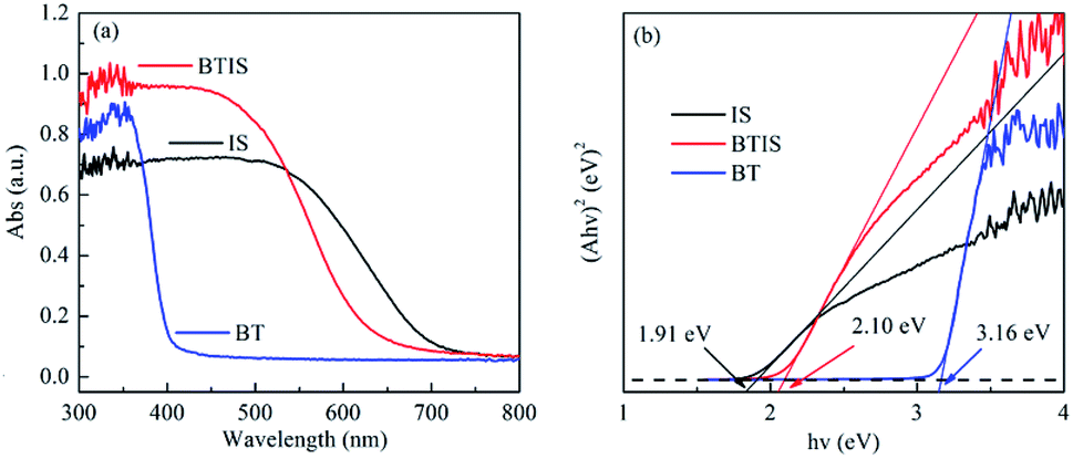 | ||
| Fig. 5 (a) UV-vis DRS spectra and (b) Tauc plots of IS, BT and BTIS respectively. | ||
For a crystalline semiconductor, the optical absorption near the band edge follows the equation:
| α(hν) = A(hν − Eg)n/2 | (2) |
The Eg-s of IS and BT measured in this work are respectively 3.16 eV and 2.10 eV, close to those reported in ref. 30 and 34, i.e. 3.30 eV and 1.92, respectively. According to the measured Eg-s, as well as the reported EVB-s in ref. 30 and 34 of IS and BT, the ECB-s of IS and BT can be evaluated according to the following equation:
| ECB = EVB − Eg | (3) |
The evaluated ECB-s of IS and BT are −0.76 eV and 0.22 eV, respectively.
3.4 Photocatalytic activity
Fig. 6a and b shows the photocatalytic degradation and rate constant k of MO by BT, IS and BTIS. Clearly, all the three samples (BT, IS and BTIS) have no dark adsorption for MO. However, BTIS has good photocatalytic properties: decompose 93% MO in 90 min under simulated-solar-light irradiation. By comparing the photocatalytic activity of IS (degrade 84% of MO in 90 min under simulated solar light) and that of BT (nearly have no photocatalytic activity under light irradiation), it can be concluded that the photocatalytic activity of IS has been improved.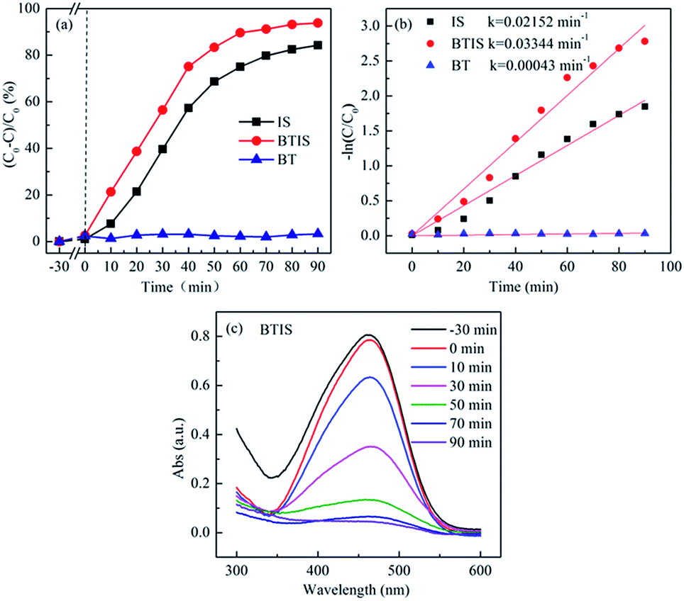 | ||
| Fig. 6 (a) Photocatalytic degradation behavior plot and (b) rate constant, k of MO by the BT, IS and BTIS respectively. (c) Time-dependent UV-vis absorption spectra of MO during photocatalytic degradation by BTIS. | ||
Photocatalytic degradation of MO roughly follows the pseudo-first-order reaction kinetics for low dye concentrations53
| ln(C0/C) = kt | (4) |
Fig. 6c gives the time-dependent UV-vis absorption spectra of MO during photocatalytic degradation by BTIS, indicating that there is no intermediates during the photocatalytic degradation of MO by BTIS if time is enough.
3.5 Ability of separation and transfer of photogenerated electron–hole pairs
The separation efficiency for photogenerated charge carriers of a semiconductor is a pivotal factor that influences its photocatalytic performance. In general, the less the PL intensity, the smaller the recombination probability of the photogenerated electron–hole pairs.6 Fig. 7a shows that PL spectra of BT, IS and BTIS under the excitation of 330 nm. It can be seen that BTIS has the lowest emission peak, indicating that BTIS possesses longest lifetime of photo-generated electron–hole pairs, probably resulting from the heterojunction in BTIS which can restrain the recombination of photogenerated electrons and holes.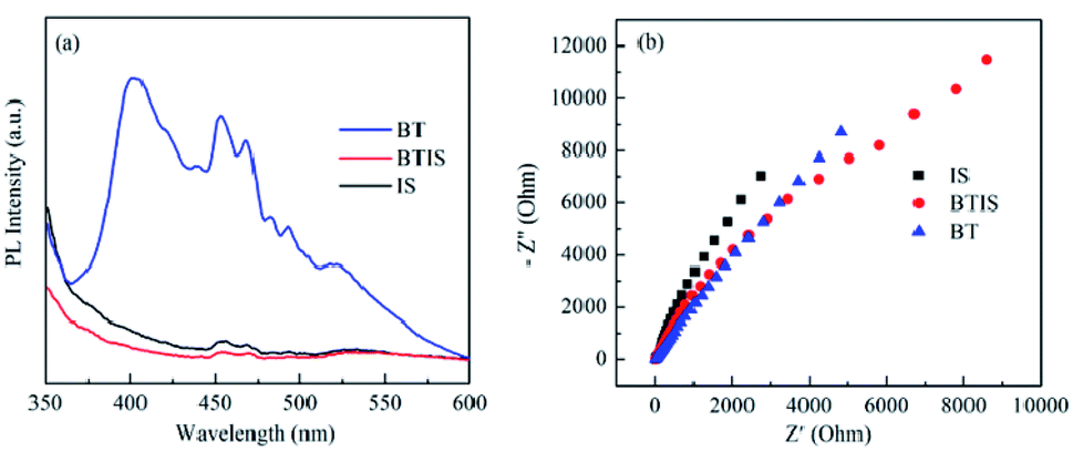 | ||
| Fig. 7 (a) Steady-state PL spectra and (b) Nyquist plot of IS, BTIS and BT, respectively. | ||
The interfacial charge migration dynamics in photocatalytic activity could be also investigated via electrochemical impedance spectroscopy (EIS).56 As shown in Fig. 7b, the arc radius on EIS Nyquist plot of BTIS is the smallest among the above-mentioned samples, suggesting that BTIS possesses the fastest interfacial charge-transfer process and more effective separation of photogenerated electron–hole pairs.54 This result is consistent with the PL result.
3.6 Photocatalysis mechanism of degrading MO over BTIS
To elucidate the contribution of reactive species to the degradation of MO by BTIS under visible light irradiation, the radical-trapping experiments with different scavengers were conducted independently. Ammonium oxalate (AO), isopropanol (IPA), benzoquinone (BQ) and carbon tetrachloride (CCl4) were used as sacrificial agent for holes (h+), hydroxyl radicals (·OH), superoxide radicals (·O2−) and electrons (e−), respectively. As indicated in Fig. 8, the addition of CCl4 (0.001 mol) and IPA (0.001 mol) has poor degradation of MO that signifies that e− and ·OH are not the main active species. However, after the addition of AO (11.8 mg) or BQ (1.2 mg), the degradation efficiency of MO was drastically suppressed, implying that the h+ and ·O2− are the predominant active species in the photocatalytic reaction process.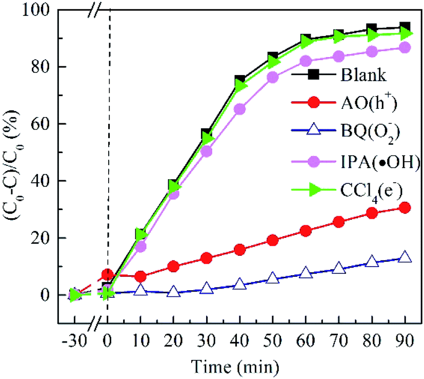 | ||
| Fig. 8 Effect of different scavengers on the MO photodegradation by BTIS. | ||
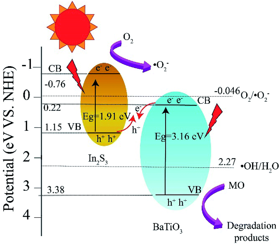
On the basis of the above experimental results, a mechanism of photocatalytic degradation of MO over BTIS is proposed as follows. As depicted in Fig. 9, the CB and VB of IS are −0.76 eV and 1.15 eV,30 respectively; while those of BT are 0.22 eV and 3.38 eV,34 respectively. Consequently, the heterojunctions BT/IS in BTIS formed Z-scheme band structures.1 Under visible light irradiation, the In2S3 acted as a sensitizer to absorb light, while the electrons in the VB-s of IS and BT in BTIS respectively jumped to the CB-s of IS and BT and left behind holes in their VB-s. And the photoinduced electrons in CB of BT tend to recombine with the photogenerated holes in VB of IS through the interface of the heterojunction BT/IS,1 leaving behind electrons in the CB of IS, holes in the VB of BT. Due to the large difference between ECB of IS (−0.76 eV) and EVB of BT (3.38 eV), a large internal electric field would produce in the heterojunctions BT/IS, resulting good separation of photoproduced electrons and holes and therefore, longer lifetime of photoinduced carriers.
 | ||
| Fig. 9 Band energy structure of heterojunction BT/IS and possible mechanism of photocatalytic degradation of MO over BTIS. | ||
On the other hand, the ECB of IS is much more negative than the standard redox potential of O2/·O2− (−0.046 eV vs. NHE). Therefore, the photogenerated electrons in the CB of IS efficiently reduced the absorbed O2 to produce ·O2−. The produced ·O2− possess strong oxidation ability to degrade organic dyes. On the other hand, the photogenerated holes left on the VB of BT possess much high positive potential and much more positive than redox potential ·OH/H2O, it would possess high oxidizing ability for MO and high-concentration-produced ·OH. The scavenger trapping experiments indicates that there are considerable ·O2−-s and h+-s, but less e− and ·OH-s, suggesting nearly all of e−-s came to the surface of BTIS and had reacted with O2, therefore produced ·O2−. But the OH− was shelt from IS, there isn't hardly the following reaction: h+ + OH− → ·OH. It is assumed that if the structure of BTIS is composites, not core–shell structure, ·OH could be produced during photocatalysis and therefore, a higher photocatalytic efficiency would be obtained.
4. Conclusion
In this work, a core–shell-heterojunction-structured Z-scheme system BaTiO3@In2S3 (labelled as BTIS) was prepared through hydrothermal method, where the commercial BaTiO3 was used as core and In(NO3)3·xH2O as well as thioacetamide was applied as the starting materials of In2S3. The as-prepared BTIS possesses the higher photocatalytic degradation capability for MO than the commercial BaTiO3 and as-prepared In2S3 (IS) fabricated by the same parameters as BTIS. Hole (h+) and superoxide radicals (·O2−) were found to be the dominant active species for BTIS. In this work, the core–shell structure has inhibited the production of ·OH because the shell In2S3 has shielded the OH− from h+, therefore inhibit the following reaction: h+ + OH− → ·OH. Opens a new pathway for designing Z-scheme photocatalyst and offers new insight into Z-scheme mechanism for applications in the field of photocatalysis.Conflicts of interest
There are no conflicts to declare.Acknowledgements
The authors gratefully acknowledge financial support from the National Natural Science Foundation of China (Grant No. 51672090 and 51372092) and the Scientific and Technological Plan of Guangdong Province (2018A050506078).Notes and references
- Y. Wang, Q. Wang, X. Zhan, F. Wang, M. Safdar and J. He, Nanoscale, 2013, 5, 8326 RSC.
- J. Qin and H. Zeng, Appl. Catal., B, 2017, 209, 161–173 CrossRef CAS.
- C. Du, J. Zhou, F. Li, W. Li, Y. Wang and Q. He, Appl. Phys. A, 2016, 122, 714 CrossRef.
- T. Xu, L. Zhang, H. Cheng and Y. Zhu, Appl. Catal., B, 2011, 101, 382–387 CrossRef CAS.
- J. Zhang, Z. Xiong and X. S. Zhao, J. Mater. Chem., 2011, 21, 3634 RSC.
- C. Du, D. Li, Q. He, J. Liu, W. Li, G. He and Y. Wang, Phys. Chem. Chem. Phys., 2016, 18, 26530–26538 RSC.
- Z. Chen, W. Zhong, Z. Liang, W. Li, G. He, Y. Wang, W. Li, Y. Xie and Q. He, J. Nanomater., 2014, 1–9 Search PubMed.
- X. Yan, K. Yuan, N. Lu, H. Xu, S. Zhang, N. Takeuchi, H. Kobayashi and R. Li, Appl. Catal., B, 2017, 218, 20–31 CrossRef CAS.
- X. Xu, X. Ding, X. Yang, P. Wang, S. Li, Z. Lu and H. Chen, J. Hazard. Mater., 2019, 364, 691–699 CrossRef CAS PubMed.
- C. Karunakaran, P. Vinayagamoorthy and J. Jayabharathi, Powder Technol., 2014, 254, 480–487 CrossRef CAS.
- T. Hu, P. Li, J. Zhang, C. Liang and K. Dai, Appl. Surf. Sci., 2018, 442, 20–29 CrossRef CAS.
- Z. Dong, Y. Wu, N. Thirugnanamc and G. Li, Appl. Surf. Sci., 2018, 430, 293–300 CrossRef CAS.
- S. Wang, B. Zhu, M. Liu, L. Zhang, J. Yua and M. Zhou, Appl. Catal., B, 2019, 243, 19–26 CrossRef CAS.
- Y. Zou, J. Shi, D. Ma, Z. Fan, C. Niu and L. Wang, ChemCatChem, 2017, 9, 3752–3761 CrossRef CAS.
- Z. Wei, Y. Wang, Y. Li, L. Zhang, H. Yao and Z. Li, J. CO2 Util., 2018, 28, 15–25 CrossRef CAS.
- H. Tong, S. Ouyang, Y. Bi, N. Umezawa, M. Oshikiri and J. Ye, Adv. Mater., 2012, 24, 229–251 CrossRef CAS PubMed.
- E. Casbeer, V. K. Sharma and X. Z. Li, Sep. Purif. Technol., 2012, 87, 1–14 CrossRef CAS.
- H. Park, Y. Park, W. Kim and W. Choi, J. Photochem. Photobiol., C, 2013, 15, 1–20 CrossRef CAS.
- D. J. Kim and W. K. Jo, Appl. Catal., B, 2019, 242, 171–177 CrossRef CAS.
- H. Zhou, Z. Wen, J. Liu, J. Ke, X. Duan and S. Wang, Appl. Catal., B, 2019, 242, 76–84 CrossRef CAS.
- Y. He, L. Zhang, M. Fan, X. Wang, M. L. Walbridge, Q. Nong, Y. Wu and L. Zhao, Sol. Energy Mater. Sol. Cells, 2015, 137, 175–184 CrossRef CAS.
- W. Dong, Y. Liu, G. Zeng, S. Zhang, T. Cai, J. Yuan, H. Chen, J. Gao and C. Liu, J. Colloid Interface Sci., 2018, 518, 156–164 CrossRef CAS PubMed.
- S. Zeng, P. Kar, U. K. Thakur and K. Shankar, Nanotechnology, 2018, 29(5), 052001 CrossRef PubMed.
- M. Akita, T. Koike and A. Inagaki, J. Synth. Org. Chem., Jpn., 2014, 72(5), 538–547 CrossRef CAS.
- W. P. To, T. Zou, R. W. Y. Sun and C. Che, Philos. Trans. R. Soc., A, 2013, 371, 20120126 CrossRef PubMed.
- Y. Gong, X. Quan, H. Yu and S. Chen, Appl. Catal., B, 2017, 219, 439–449 CrossRef CAS.
- Q. Xu, L. Zhang, J. Yu, S. Wageh, A. Al-Ghamdi and M. Jaroniec, Mater. Today, 2018, 21, 10 Search PubMed.
- D. Tsukamoto, M. Ikeda, Y. Shiraishi, T. Hara, N. Ichikuni, S. Tanaka and T. Hirai, Chem.–Eur. J., 2011, 17, 9816–9824 CrossRef CAS PubMed.
- A. Fujishima, T. N. Rao and D. A. Tryk, J. Photochem. Photobiol., C, 2000, 1, 1–21 CrossRef CAS.
- J. Luo, X. Zhou, X. Ning, L. Zhan, L. Ma, X. Xu, Z. Huang and J. Liang, New J. Chem., 2017, 41, 845 RSC.
- J. Luo, X. Zhou, X. Ning, L. Zhan, L. Huang, Q. Cai, S. Li and S. Sun, Mater. Res. Bull., 2018, 100, 102–110 CrossRef CAS.
- F. Guo, W. Shi, M. Li, Y. Shi and H. Wen, Sep. Purif. Technol., 2019, 210, 608–615 CrossRef CAS.
- J. Shi, S. Li, F. Wang, Y. Li, L. Gao, X. Zhang and J. Lu, Catal. Sci. Technol., 2018, 8, 6458 RSC.
- Y. Xu and M. A. A. Schoonen, Am. Mineral., 2000, 85, 543–556 CrossRef CAS.
- W. Zhong, Y. Yu, C. Du, W. Li, Y. Wang, G. He, Y. Xie and Q. He, RSC Adv., 2014, 4, 40019 RSC.
- Z. Chen, H. Jiang, W. Jin and C. Shi, Appl. Catal., B, 2016, 180, 698–706 CrossRef CAS.
- C. D. Wagner, W. M. Riggs, L. E. Davis, J. F. Moulder and G. E. Muilenberg, Surf. Interface Anal., 1981, 3, 4 CrossRef.
- H. McDaniel, P. E. Heil, C. L. Tsai, K. Kim and M. Shim, ACS Nano, 2011, 5(9), 7677–7683 CrossRef CAS PubMed.
- S. Meng, W. Sun, S. Zhang, X. Zheng, X. Fu and S. Chen, J. Phys. Chem. C, 2018, 122(46), 26326–26336 CrossRef CAS.
- R. Scheer and H. J. Lewerenz, J. Vac. Sci. Technol., A, 1994, 12, 56 CrossRef CAS.
- A. Gheorghiu, I. Lampre, S. Dupont, C. Sénénaud, M. A. E. I. Raghni, P. E. Lippens and J. Olivier-Fourcade, J. Alloys Compd., 1995, 228, 143–147 CrossRef CAS.
- D. E. Fowler and D. C. Miller, Surf. Sci. Spectra, 1992, 1, 381 CrossRef CAS.
- B. Ghosh, A. Dutta, S. Shannigrahi and T. P. Sinha, J. Alloys Compd., 2015, 648, 111–115 CrossRef CAS.
- A. P. Dementjev, O. P. Ivanova, L. A. Vasilyev, A. V. Naumkin, D. M. Nemirovsky and D. Y. Shalaev, J. Vac. Sci. Technol., A, 1994, 12, 423 CrossRef CAS.
- D. Gonbeau, C. Guimon, G. Pfister-Guillouzo, A. Levasseur, G. Meunier and R. Dormoy, Surf. Sci., 1991, 254, 81–89 CrossRef CAS.
- H. Ikawa, T. Yamada, K. Kojima and S. Matsumoto, J. Am. Ceram. Soc., 1991, 74(6), 1459–1462 CrossRef CAS.
- P. Senthilkumar, S. Dhanuskodi, M. Muneeswaran, N. V. Giridharan, S. Kuila and P. N. Vishwakarma, J. Appl. Phys., 2018, 123, 244101 CrossRef.
- P. Ren, H. Fan and X. Wang, Appl. Phys. A, 2013, 111, 1139–1145 CrossRef CAS.
- M. A. Stranick, M. Houalla and D. M. Hercules, J. Catal., 1987, 106, 362–368 CrossRef CAS.
- N. Gunasekaran, S. Rajadurai, J. J. Carberry, N. Bakshi and C. B. Alcock, Solid State Ionics, 1994, 73, 289–295 CrossRef CAS.
- V. I. Bukhtiyarov, A. I. Boronin and V. I. Savchenko, J. Catal., 1994, 150, 262–267 CrossRef CAS.
- S. Selvarajan, P. Malathy, A. Suganthi and M. Rajarajan, J. Ind. Eng. Chem., 2017, 53, 201–212 CrossRef CAS.
- J. Yu, G. Wang, B. Cheng and M. Zhou, Appl. Catal., B, 2007, 69, 171–180 CrossRef CAS.
- Z. Qiao, T. Yan, W. Li and B. Huang, New J. Chem., 2017, 41, 3134 RSC.
- T. Xian, H. Yang, L. J. Di and J. F. Dai, J. Alloys Compd., 2015, 622, 1098–1104 CrossRef CAS.
- F. Meng, Y. Liu, J. Wang, X. Tan, H. Sun, S. Liu and S. Wang, J. Colloid Interface Sci., 2018, 532, 321–330 CrossRef CAS PubMed.
| This journal is © The Royal Society of Chemistry 2019 |