
 Open Access Article
 This Open Access Article is licensed under a Creative Commons Attribution-Non Commercial 3.0 Unported Licence
Mid-infrared GaAs/AlGaAs micro-ring resonators characterized via thermal tuning
Julian Haas ,
Philipp Artmann and
Boris Mizaikoff*
,
Philipp Artmann and
Boris Mizaikoff*
Institute of Analytical and Bioanalytical Chemistry, Ulm University, Albert-Einstein-Allee 11, D-89081 Ulm, Germany. E-mail: boris.mizaikoff@uni-ulm.de
First published on 14th March 2019
Abstract
Micro-ring resonators with a decoupling waveguide have been manufactured from GaAs/Al0.2Ga0.8As, accommodating mid-infrared wavelengths, and were characterized via thermal tuning. A Q-factor of 1900, a thermal full width at half maximum of 8 °C, and a thermal free spectral range of 18 °C have been achieved. The low Q-factor indicates comparatively high coupling efficiency from the input waveguide into the decoupling waveguide. The micro-ring resonators shown herein are suitable structures for advanced mid-infrared chem/bio sensing strategies via resonant-cavity enhancement. In addition, they offer high spectral resolution for evanescent field sensing strategies via effective wavelength de-multiplexing waveguide structures.
Introduction
Optic circuitry in the visible spectral regime enabling, e.g., integrated on-chip sensing applications is dominated by silicon and related silicon-on-insulator (SOI) CMOS compatible designs.1–3 A wide variety of logical gates and de-multiplexing elements such as single beam splitters, multiple beam splitters, and Mach–Zehnder interferometer (MZI) structures are deployed for, e.g. wavelength de-multiplexing. Micro-ring resonators are straight forward optical structures, enabling decoupling of radiation at a precisely defined wavelength, either determined by the ring dimensions4 or controlled via precise refractive index tuning, e.g., via thermal tuning strategies.5,6 For this task, different geometries, comprising micro-toroids,7–9 whispering galley mode resonators (e.g., micro-disks), and designs with elongated coupling regions such as race-track, sling or pulley couplers have demonstrated effective operation.However, such devices are virtually exclusively tailored for and limited to telecom wavelengths, i.e., the near infrared (NIR) around 1.3–1.6 μm. Besides applications in telecommunications technology, chemical sensing via more or less sophisticated optical transducers has increasingly matured during recent years, frequently taking advantage of such structures for various sensing tasks.10,11 For example, Lechuga et al. have shown applications of MZI and bimodal waveguides for the detection of biomolecules.12,13 Also, micro-toroids have been integrated into chemical sensing tasks,14 likewise, the detection of nanoparticle aggregation has been shown for slotted ring resonators.15 Crespi et al. have shown applications utilizing more sophisticated quantum states of light, thereby harnessing sophisticated optical structures for protein sensing. However, extending chem/bio sensing schemes from the visible and NIR into the mid-infrared (MIR; 3–12 μm) spectral region has to date been limited by appropriate materials that are transparent in this spectral window.16–19 Chem/bio sensing via the evanescent field emanating from the waveguide structure especially benefits from extending the wavelength of the utilized radiation into the MIR. Since the penetration depth of the evanescent field into an adjacent analyte matrix directly depends on the wavelength of the utilized radiation, the evanescent field in the MIR extends up to several μm away from the waveguide surface. In comparison to visible and NIR frequencies, an increased analyte volume is probed, which enables detecting minute analyte quantities at improved limits of detection.
Recently, a silicon-on-sapphire (SOS) ring resonator concept has been shown operating at wavelengths ranging from 2.75 μm (ref. 20 and 21) to 5.5 μm (ref. 22) and 8 μm.23 Chalcogenide glass waveguides have been presented for operation around 5.2 μm (ref. 24) and germanium-based strategies have been presented for operation in the long wave mid infrared.25,26
As an alternative, the III–V semiconductor material gallium arsenide (GaAs) may be deposited onto an optical buffer layer made from aluminium gallium arsenide (AlGaAs) thus providing a possibly wide transparent window in the MIR (i.e., 0.9–25 μm), as pioneered by Mizaikoff and collaborators.27,28 GaAs/AlGaAs systems therefore can be utilized throughout the whole near-, mid- and far-infrared with the possibility to monolithically integrate the waveguides with sources, especially quantum cascade lasers (QCLs), and detector schemes. What is more, AlGaAs represents a readily available buffer layer as the design for adequate lower refractive index cladding layers can be challenging for chalcogenide classes. A variety of applications using slab and ridge waveguides, as well as a thin-film MIR-MZI designs have been demonstrated and applied in exemplary chem/bio sensing scenarios.29–32 Based on design studies by Sieger et al.,33 GaAs/AlGaAs MIR thin-film waveguide structures may readily be designed and optimized for single-mode propagation.
Experimental
Simulation
The micro-ring resonators presented in this study were optimized for a resonance frequency around 6 μm.In this spectral region, various biologically relevant analytes such as proteins are characterized by pronounced and molecularly selective absorption features. Hence, cavity-enhanced sensing schemes, enabling ultra-sensitive analysis or high-resolution wavelength splitting, facilitating advanced absorption spectroscopy based chem/bio sensing schemes may be realized via the presented structures, and may be extended into the fingerprint spectral regime (>10 μm) for other analytes in the future. Theoretical modelling of wavelength dependent transmission properties of the presented resonator structures was merged with temperature dependent transmission spectra of waveguide structures that were subsequently manufactured according to the developed design input.
The basic design parameters (free spectral range, FSR; full width at half maximum, FWHM) of optical micro-ring resonators derive as shown in eqn (1) and (2)
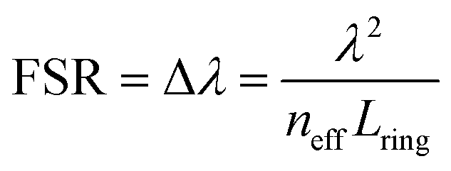 | (1) |
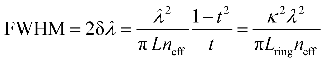 | (2) |
![[thin space (1/6-em)]](https://www.rsc.org/images/entities/char_2009.gif) 500 can be derived using eqn (3)
500 can be derived using eqn (3)
 | (3) |
For a more precise approximation of the expectable resonance behaviour, finite element method (FEM) calculations were performed using COMSOL Multiphysics considering a waveguide thickness of 6 μm and a coupling trench width of 200 nm. A wavelength resolution of Δλ = 33 pm was selected to accurately model and resolve the expected spectral features (Fig. 1). For a ring resonator without an additional decoupling port, a FWHM of 0.45 nm or 0.12 cm−1, respectively, was calculated, which translates into a theoretical Q-factor of approx. 13000 at a centre wavelength of 5.99 μm. For a ring resonator with an additional decoupling port, a FWHM of 0.23 nm or 0.07 cm−1, respectively, was calculated, which gives rise to a theoretical Q-factor of approx. 25000 at a centre wavelength of 5.96 μm. Furthermore, the transmission intensity at the resonance frequency is reduced by approx. 32% in both cases. Due to the idealized model, the all-pass resonator without any de-coupling port represents an over-coupled resonator in which excess energy is coupled back from the ring into the waveguide (Fig. 1(a) and (b)). As a result, fewer round-trips are possible and a broader bandwidth is coupled into the ring, leading to a broader FWHM and a lower Q-factor in comparison to the micro-ring resonator with an out-coupling port. The additional out-coupling port (add-drop configuration) reduces back-coupling into the in-coupling port and thus leads to a narrower FWHM of the resonance dip and a higher Q-factor, respectively (Fig. 1(c) and (d)). The derived values for the FWHM and Q-factors are well in agreement with the values calculated via eqn (1) and (2), which confirms that these models are valid for the waveguide structures designed herein.
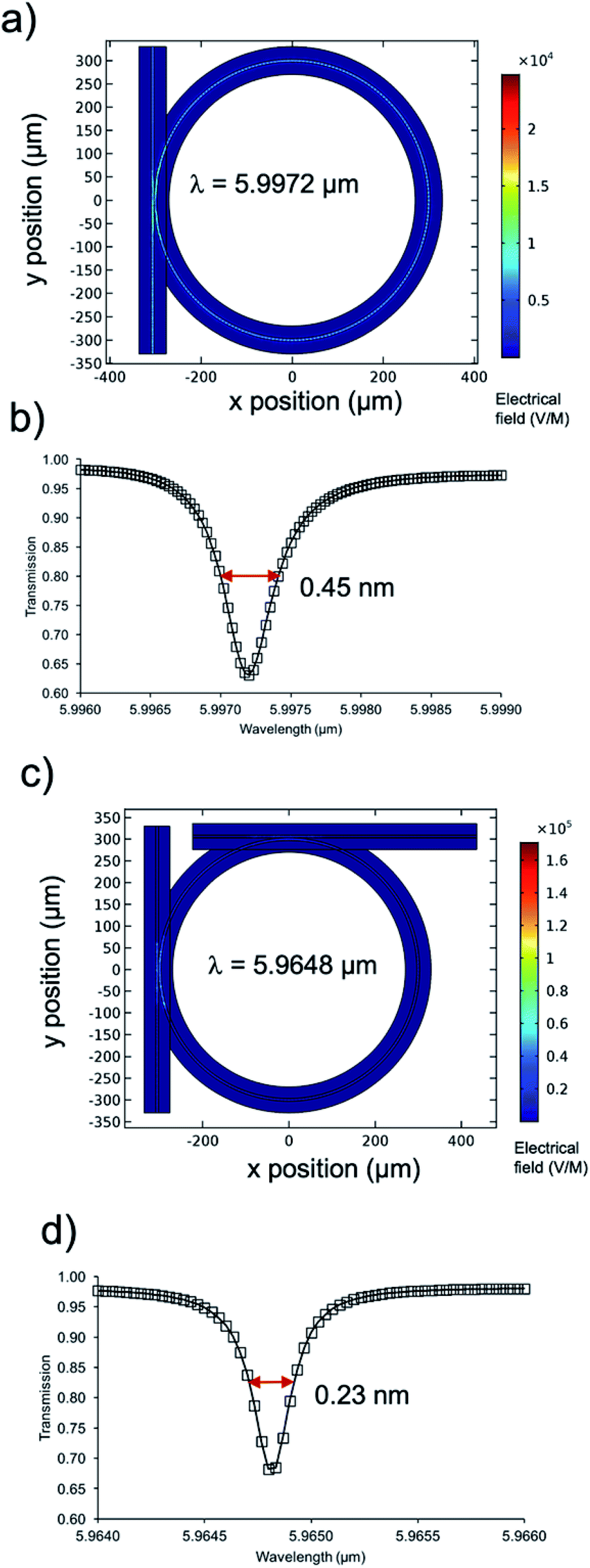 | ||
| Fig. 1 (a) 2D FEM simulation of a 6 μm GaAs micro-ring resonator showing the electrical field intensity. (b) Resonance dip for the plotted transmission of the throughput port of the structure shown in (a). (c) FEM simulated electrical field intensity for a micro-ring resonator with an out-coupling port. (d) Corresponding resonance dip at the throughput port of the structure shown in (c). | ||
Waveguide fabrication
GaAs waveguide structures with a thickness of 6 μm were epitaxially grown onto a 6 μm buffer layer of Al0.2Ga0.8As, which was deposited onto a heavily n-doped GaAs substrate wafer.The waveguides structures were patterned via photolithography and via reactive ion etching (RIE) using SiCl4/Ar dry chemistry. In brief, the photoresist (AZ ECI 3027, Allresist GmbH, Strausberg, Germany) was spin-coated onto the wafer, exposed via a manual mask aligner (SUSS-MJB3, Suss Microtec GmbH, Garching, Germany), and developed in a puddle (AZ MIF 726, Allresist GmbH, Strausberg, Germany) for defining the waveguide structures via the photoresist. Final waveguide patterning was achieved via reactive ion etching (RIE) using SiCl4/Ar dry chemistry (10 sccm/6 sccm, 35 W RF, p = 15 mTorr, Plasmalab System 100, Oxford Plasmalab, Yatton, UK). The precise definition of the coupling trench was achieved via focused ion beam (FIB) milling (Quanta 3D FEG, FEI Eindhoven, Netherlands). After fabrication of the waveguides, the coupling facets were cleaved using a diamond knife facilitating effective in-coupling from free space.
Finally obtained waveguides comprised a tapered in-coupling region, a straight section with the ring-resonator, and a straight out-coupling waveguide oriented perpendicular to the in-coupling waveguide structure.
Fig. 2 gives an example of a GaAs micro-ring resonator (6 μm wide, 6 μm high) with a diameter of approx. 496 μm, and a length of approx. 1450 μm along with alignment waveguides, in-coupling waveguide, and de-coupling waveguide (a). Fig. 2(b) shows the front view of a cleaved GaAs waveguide facet (6 × 6 μm) deposited onto an Al0.2Ga0.8As buffer layer (thickness 6 μm) revealing a neat end facet with minimal scattering losses.
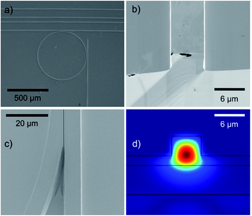 | ||
| Fig. 2 (a) Example of a GaAs micro-ring resonator along with alignment waveguides, as well as in-coupling and de-coupling waveguides. (b) Skewed top and front view of an end-facet and the top side of a tilted GaAs waveguide (6 μm × 6 μm) deposited onto an Al0.2Ga0.8As buffer layer (6 μm). (c) Magnified view of a FIB-milled coupling trench with a spacing of approx. 200 nm. (d) FEM simulation of the confined electrical field (λ = 6 μm) within a 6 μm × 6 μm GaAs waveguide modelled on top of an Al0.2Ga0.8As buffer layer, which forms a rib due to potential incomplete etching of the GaAs layer within coupling trenches. | ||
Furthermore, the substrate was heavily n-doped ensuring its opaqueness in the MIR, and thus, reducing light scattering or coupling into the substrate. Fig. 2(c) reveals a close-up view of a FIB-milled coupling trench with a spacing of approx. 200 nm. However, due to re-deposition during the FIB-milling process slightly V-shaped sidewalls are to be expected. Hence, the formation of waveguide ribs is likely. Fig. 2(d) shows a complementary FEM simulation of the confined electrical field at a wavelength of 6 μm within a 6 × 6 μm GaAs waveguide modelled on top of a Al0.2Ga0.8As buffer layer, which forms a 2 μm rib waveguide due to incomplete etching of the GaAs layer. The calculated pronounced confinement of the electrical field within the 6 μm structure ensures that evanescent field coupling to the resonator is enabled.
Waveguide characterization
Linear polarized (100:1) radiation was provided by a broadly tuneable external cavity quantum cascade laser (EC-QCL, Mircat 1000-7603, Daylight Solutions Inc., San Diego, USA) operated in continuous wave (cw) mode with a typical, manufacturer given, linewidth of <0.003 cm−1 or about 0.01 nm at a wavelength of 6 μm, respectively. Emanating radiation at the distal end of the waveguide structure was detected via a liquid nitrogen cooled (LN2) mercury-cadmium-telluride (MCT) semiconductor detector (Kolmar Technologies Inc., Newburyport, USA).
Thermal tuning was performed via an external resistive heating device (Watlow EZ-Zone, Watlow GmbH, Kronau, Germany). The temperature was monitored using a type K NiCrNi thermocouple. Both, intensity and temperature data were recorded via an AD converter (NI USB-9162 National Instruments GmbH, München, Germany), and a custom control software programmed in Labview (Labview 2014, SP1, V 14.0f3, National instruments GmbH, München, Germany). A schematic layout of the experimental setup is shown in Fig. 3.
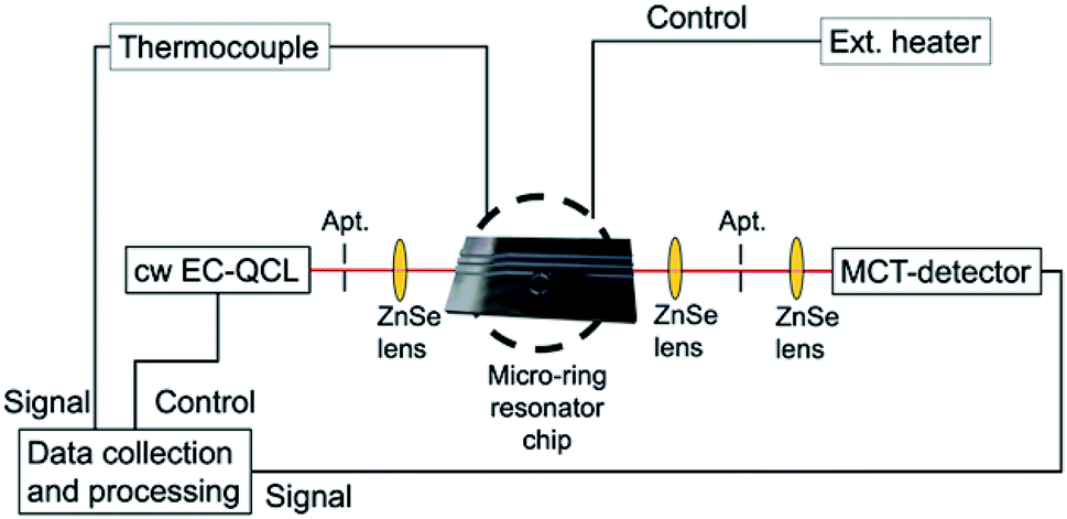 | ||
| Fig. 3 Scheme of the experimental setup comprising a cw EC-QCL, a MCT-detector, an external heating system, and a thermocouple. Incident radiation is shaped via apertures and focused onto the waveguide facet using zinc selenide (ZnSe) lenses. Micro-ring resonator chip, electrical heater, and the thermocouple are in thermal contact. | ||
Results & discussion
Since the calculated narrow resonance dips of micro-ring resonators impose highly precise tuning and high wavelength resolution on the QCL, temperature tuning has been introduced by Tsang et al.21 as powerful strategy for estimating micro-ring resonator characteristics at single wavelength emission via precise temperature tuning of the resonant cavity. While this was readily achieved using conventional temperature controller units, propagation losses and temperature dependency of the coupling efficiency between the waveguides and the ring structure were assumed to be temperature independent in the evaluated temperature range in this simplified model. Furthermore, the linear coefficient of thermal expansion of GaAs is in the order of 10−6 K−1,34 which is two orders of magnitude lower than the thermo-optic coefficient of GaAs and therefore neglectable in the performed analysis. Moreover, thermo-optic effects of AlGaAs are assumed to be negligible (i.e., thermo-optic effect of GaAs of ∂n/∂T = 2.35 × 10⁻⁴ (ref. 35)). In analogy to wavelength tuning, the determination of a Q-factor via eqn (4) has been derived as
 | (4) |
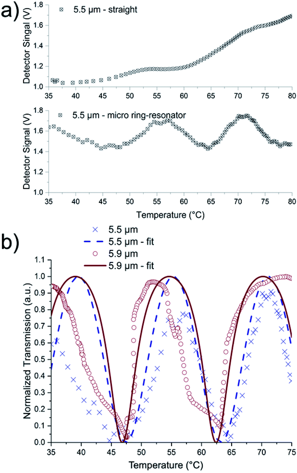 | ||
| Fig. 4 (a) Transmission behaviour of a straight waveguide only without pronounced dips vs. a waveguide with a coupled micro-ring resonator. (b) Resonance behaviour during thermal tuning exemplarily shown at two selected wavelengths, corrected by the transmission behaviour of a straight waveguide at the respective wavelength to correct for non-ring related transmission characteristics. | ||
Furthermore, a roundtrip loss factor of α = 0.4 ± 0.1, and a field coupling coefficient of t = 0.6 ± 0.2 was derived. However, the temperature tuning curves are superimposed by arbitrary spikes of the detected intensity that can be assigned to mode-hops and emission instabilities of the QCL resulting from random fluctuations in laser chip temperature and applied current appearing randomly during cw operation at a fixed wavelength (i.e. at non-stabilized operation conditions). Apart from the ideal, potentially possible, laser linewidth of <0.003 cm−1 (about 0.01 nm at 6 μm), an effective linewidth, that can be mainly attributed to mode-hopping, may reach dimensions of up to 0.1 cm−1 (0.4 nm at 6 μm) that limits the experimentally obtainable Q-factor, especially, when attempting to tune the QCL emission wavelength. It is anticipated that devices with stabilized emission intensity or mode-hop-free lasers provide increased Q-factors; hence, it is safe to assume that the Q-factors derived herein are underestimated.
Potential optical scattering losses, e.g. due to rough waveguide sides, or process imperfections, can lead to a reduced experimentally obtainable Q-factor in comparison to the value obtained from the ideal simulation. The rather low Q-factors may be associated with the rather high losses as well as with the decoupling waveguide and indicate apparently efficient decoupling. With the derived values of 0.4 for the roundtrip loss factor α and 0.6 for the field coupling coefficient t, the ring represents an over-coupled case. In this case, light will be coupled back from the ring into the in-coupling waveguide, which leads to a broadened FWHM, i.e. a broader bandwidth that is coupled into the ring as for critical coupling case (α = t). It was shown that approx. 22% of the detected signal intensity was coupled from the straight waveguide at the resonance wavelength, which is in the range previously calculated (33%) and indicates successful yet improvable decoupling. Since, over-coupling is presumed to be the main reason for the low experimental Q-factor, improved designs for designing the orientation of the de-coupling port, i.e. parallel to the in-coupling port or in a pulley like configuration may lead to improved Q-factors in further studies.
In this context, extended optimization of the coupling gap dimensions, i.e. width, length (e.g. race track designs) and depth (e.g. slab-like designs), both theoretically and experimentally, may lead to further improved Q-factors as well as an improved insight into the resonator behaviour.
With optimized micro-ring resonator structures, chem/bio sensing may be achieved by utilizing tunable laser light sources providing sufficient spectral resolution in order to evaluate minute resonance peak shifts within the resonance spectra. In such sensing scenarios, shifts of the wavelength position at resonance arise from analyte exposure of the waveguide changing the effective refractive index (neff). Consequently, the resonance peak shows an analyte concentration dependent shift. Appropriate surface modification of the waveguide with chem/bio recognition motifs may further enhance analyte interactions in close vicinity of the waveguiding structure, thereby resulting in an even more pronounced refractive index variation yielding an improved analytical sensitivity.
Conclusions
Thin-film micro-ring resonators have been designed, fabricated and were characterized via thermal tuning of the resonator structure. The derived Q-factors of the GaAs/AlGaAs rings was approx. 1900.The limited spectral resolution of the deployed EC-QCL light source was mitigated by the thermal tuning method. In future, similar studies using light sources with increased spectral resolution such as mode-hop-free (MHF)-QCLs or frequency combs enable further verification of the applied characterization method for evaluating the potential utility of MIR thin-film micro-resonators for chem/bio sensing applications via resonant-cavity enhancement and via de-multiplexed waveguide structures. In addition, the presented micro-ring resonators are a first step towards even more sophisticated photonic structures based on a GaAs/Al0.2Ga0.8As waveguide architectures. Further evaluation of the transmission characteristics, chem/bio sensing behaviour, and properties of straight, curved or more complex coupled structures will benefit from the findings provided herein.
Conflicts of interest
There are no conflicts to declare.Acknowledgements
This study has in part been funded by the European Union's Seventh Framework Programme managed by REA Research Executive Agency http://ec.europa.eu/rea (FP7/2007-2013) under Grant Agreement No. 314018 FP7-SME-2012-SME (MYCOSPEC) and by the H2020-ICT-2016-2017 project MIRACLE (#780598) funded by the European Union. The Focused Ion Beam Center UUlm supported by the FEI Company (Eindhoven, The Netherlands), the German Science Foundation (INST40/385-F1UG), and the Struktur- und Innovationsfonds Baden-Württemberg is thanked for FIB-based prototyping. Finally, the Centre for Integrated Quantum Science and Technology (IQST), Ulm University, University of Stuttgart, and MPI for Solid State Research, Germany are acknowledged for supporting this study.References
- R. Soref, IEEE J. Sel. Top. Quantum Electron., 2006, 12(6), 1678–1687 CAS.
- B. Jalali and S. Fathpour, J. Lightwave Technol., 2006, 24(12), 4600–4615 CAS.
- M. Li, W. H. P. Pernice, C. Xiong, T. Baehr-Jones, M. Hochberg and H. X. Tang, Nature, 2008, 456(7221), 480–484 CrossRef CAS PubMed.
- A. Yariv, IEEE Photonics Technol. Lett., 2002, 14(4), 483–485 Search PubMed.
- X. Zheng, I. Shubin, G. Li, T. Pinguet, A. Mekis, J. Yao, H. Thacker, Y. Luo, J. Costa, K. Raj, J. E. Cunningham and A. V. Krishnamoorthy, Opt. Express, 2010, 18(5), 5151 CrossRef CAS PubMed.
- I. Shubin, X. Zheng, G. Li, H. Thacker, J. Yao, B. Guenin, T. Pinguet, A. Mekis, a. V. Krishnamoorthy and J. E. Cunningham, Proc. SPIE, 2011, 7944(11), 794402 CrossRef.
- D. K. Armani, T. J. Kippenberg, S. M. Spillane and K. J. Vahala, Nature, 2003, 421, 925–928 CrossRef CAS PubMed.
- X. Zhang and A. M. Armani, Opt. Express, 2013, 21(20), 23592–23603 CrossRef CAS PubMed.
- P. Del'Haye, A. Schliesser, O. Arcizet, T. Wilken, R. Holzwarth and T. J. Kippenberg, Nature, 2007, 450(7173), 1214–1217 CrossRef PubMed.
- Y. Sun and X. Fan, Anal. Bioanal. Chem., 2011, 399(1), 205–211 CrossRef CAS PubMed.
- A. Yalcin, K. C. Popat, J. C. Aldridge, T. A. Desai, J. Hryniewicz, N. Chbouki, B. E. Little, O. King, V. Van, S. Chu, D. Gill, M. Anthes-Washburn, M. S. Unlu and B. B. Goldberg, IEEE J. Sel. Top. Quantum Electron., 2006, 12(1), 148–155 CAS.
- M. C. Estevez, M. Alvarez and L. M. Lechuga, Laser Photonics Rev., 2012, 6(4), 463–487 CrossRef.
- D. Duval and L. M. Lechuga, IEEE Photonics J., 2013, 5(2), 0700906 Search PubMed.
- A. M. Armani, R. P. Kulkarni, S. E. Fraser, R. C. Flagan and K. J. Vahala, Science, 2007, 317(5839), 783–787 CrossRef CAS PubMed.
- J. Witzens and M. Hochberg, Opt. Express, 2011, 19(8), 7034 CrossRef CAS PubMed.
- X. Wang, M. Sieger and B. Mizaikoff, Proc. SPIE, 2013, 8631, 86312M CrossRef.
- M. Sieger and B. Mizaikoff, Anal. Chem., 2016, 88(11), 5562–5573 CrossRef CAS PubMed.
- B. Mizaikoff, X. Wang, M. Sieger, L. Faraone, J. Antoszewski, W. Lei, M. Jetter and P. Michler, in 2014 Conference on Optoelectronic and Microelectronic Materials & Devices, IEEE, 2014, pp. 301–302 Search PubMed.
- B. Mizaikoff, Chem. Soc. Rev., 2013, 42(22), 8683 RSC.
- C. Y. Wong, Z. Cheng, X. Chen, K. Xu, C. K. Y. Fung, Y. Chen and H. K. Tsang, IEEE Photonic Soc. 24th Annu. Meet. PHO 2011, 2011, vol. 5, pp. 877–878 Search PubMed.
- C. Y. Wong, Z. Cheng, X. Chen, K. Xu, C. K. Y. Fung, Y. M. Chen and H. K. Tsang, IEEE Photonics J., 2012, 4(4), 1095–1102 Search PubMed.
- A. Spott, Y. Liu, T. Baehr-Jones, R. Ilic and M. Hochberg, Appl. Phys. Lett., 2010, 97(21), 213501 CrossRef.
- Z. Cheng, X. Chen, C. Y. Wong, K. Xu and H. K. Tsang, IEEE Photonics J., 2012, 4(5), 1510–1519 Search PubMed.
- P. Ma, D.-Y. Choi, Y. Yu, Z. Yang, K. Vu, T. Nguyen, A. Mitchell, B. Luther-Davies and S. Madden, Opt. Express, 2015, 23(15), 19969 CrossRef CAS PubMed.
- S. Radosavljevic, N. T. Beneitez, A. Katumba, M. Muneeb, M. Vanslembrouck, B. Kuyken and G. Roelkens, Opt. Mater. Express, 2018, 8(4), 824 CrossRef.
- J.-M. Fédéli, P. Labeye, A. Marchant, O. Lartigue, M. Fournier and J.-M. Hartmann, in Silicon Photonics: From Fundamental Research to Manufacturing, ed. R. G. Baets, P. O'Brien and L. Vivien, SPIE, 2018, p. 21 Search PubMed.
- T. Schädle and B. Mizaikoff, Appl. Spectrosc., 2016, 70(10), 1625–1638 CrossRef PubMed.
- C. Charlton, M. Giovannini, J. Faist and B. Mizaikoff, Anal. Chem., 2006, 78(12), 4224–4227 CrossRef CAS PubMed.
- X. Wang, S.-S. Kim, R. Roßbach, M. Jetter, P. Michler and B. Mizaikoff, Analyst, 2012, 137(10), 2322 RSC.
- J. Haas, R. Stach, M. Sieger, Z. Gashi, M. Godejohann and B. Mizaikoff, Anal. Methods, 2016, 8(36), 6602–6606 RSC.
- M. Sieger, G. Kos, M. Sulyok, M. Godejohann, R. Krska and B. Mizaikoff, Sci. Rep., 2017, 7, 44028 CrossRef PubMed.
- L. Leidner, M. Ewald, M. Sieger, B. Mizaikoff and G. Gauglitz, Proc. SPIE, 2013, 8774, 87740S CrossRef.
- M. Sieger and B. Mizaikoff, Photonics Res., 2016, 4(3), 106 CrossRef CAS.
- T. Soma, J. Satoh and H. Matsuo, Solid State Commun., 1982, 42(12), 889–892 CrossRef CAS.
- F. G. Della Corte, G. Cocorullo, M. Iodice and I. Rendina, Appl. Phys. Lett., 2000, 77(11), 1614–1616 CrossRef CAS.
| This journal is © The Royal Society of Chemistry 2019 |