
 Open Access Article
 This Open Access Article is licensed under a Creative Commons Attribution-Non Commercial 3.0 Unported Licence
Study of the perpendicular self-assembly of a novel high-χ block copolymer without any neutral layer on a silicon substrate
Baolin Zhang ab,
Weichen Liub,
Lingkuan Meng*cd,
Zhengping Zhanga,
Libin Zhangb,
Xing Wue,
Junyan Daie,
Guoping Maoe and
Yayi Wei*b
ab,
Weichen Liub,
Lingkuan Meng*cd,
Zhengping Zhanga,
Libin Zhangb,
Xing Wue,
Junyan Daie,
Guoping Maoe and
Yayi Wei*b
aCollege of Big Data and Information Engineering, Guizhou University, Guiyang 550025, P. R. China
bIntegrated Circuit Advanced Process Center (ICAC), Institute of Microelectronics of Chinese Academy of Sciences (IME CAS), Beijing 100029, P. R. China. E-mail: weiyayi@ime.ac.cn; Fax: +86-10-82995684; Tel: +86-10-82995898
cThe Integrated Circuit Materials & Components Industry Technology Innovative Alliance, 27 Zhichun Road, Haidian District, Beijing 100083, P. R. China. E-mail: lingkuan_meng@icmtia.com; Tel: +86-10-82357517
dSchool of Electronic Engineering, Chengdu Technological University, Chengdu 611730, P. R. China
eJiangsu HanTop Photo-Materials Co., Ltd, Floor 4-5, Buliding No. 9, No. 1158 Zhongxin Rd, Shanghai, P. R. China
First published on 29th January 2019
Abstract
A novel type of high-χ block copolymer, polystyrene-block-polycarbonate (PS-b-PC), which contains an active –NH– group on the polymer backbone between the PS block and the PC block, has been successfully synthesized. Vertical micro-phase separation can be successfully achieved on Si substrates with neutral-layer-free materials with a pitch of 16.8 nm. Water contact angle experiments indicate that PS and PC have approximate surface energy values on Si substrates. A hydrogen bond mechanism has been proposed for the formation of a periodic and lamella-forming phase separation structure, with the domains oriented perpendicular to the substrate. A combination of both theory and experimental verification proves that the hydrogen bonding plays a dominant role as a real driving force to promote vertical micro-phase separation in the absence of a neutral layer. Subsequently, the study of a novel block copolymer on four different types of substrate without any neutral layer further confirms that the newly synthesized material enables greater flexibility and potential applications for the fabrication of various nanostructures and functional electronic devices in a simple, cost-effective and efficient way, which is of considerable importance to contemporary and emerging technology applications.
1. Introduction
Recently, interest in the patterning of self-assembly of block copolymers (BCPs) has attracted considerable attention because of their wide and promising applications in many fields of nanoscience and nanofabrication, including biomolecule detection,1 nanochannels for nanofluidic fabrication,2 nanostructure fabrication,3,4 advanced IC devices,5,6 and as a nanoimprint template to create nanopillars.7,8 These potential applications have driven extensive efforts in both academia and industry to apply the technique to achieve precisely controlled geometric size, highly aligned and ordered arrays to meet the stringent requirements for many emerging applications, especially in semiconductor IC manufacture and fabrication of some functional electronic devices. With the shrinking of the size of semiconductor devices, the traditional 193 nm immersion lithography combined with multi-patterning technology is becoming more and more complicated in 10 nm nodes and beyond. This is bound to require a novel lithography solution, such as EUV (extreme ultraviolet lithography), DSA (directed self-assembly) technology, etc. Self-assembly of BCPs combined with advantages of conventional photolithography and polymeric materials shows a great utility for semiconductors and a lot of potential applications. It does not require an optical exposure system and reticles, and therefore it is very cost-effective and attracts lots of interest. It is currently considered as a promising alternative patterning technology to extend Moore's Law for future nodes by ITRS (International Technology Roadmap for Semiconductors). In order to apply self-assembly of BCPs in semiconductor manufacture, effective micro-phase separation must be achieved. For example, lamellar phase separation BCPs can be used to fabricate fin and gate arrays in advanced FinFET devices.9,10 Vertical cylinder phase separation can be used to make contact holes or channel holes in advanced CMOS devices.11,12 The self-assembled, periodic structures of BCPs with well-defined sizes and separation distances on the tens of nanometers length scale or even a few nanometers have been recognized as a promising route for the fabrication of a wide range of functional nanostructures. By changing molecular weight, chemical structure, molecular architecture, and composition of BCPs, the size and type of self-assembly can be controlled precisely. Understanding and controlling the orientation and/or dimensions of BCP microdomains are very essential for various advanced device applications.Most research on the vertical phase separation of BCPs has been focused on utilizing neutral layers to realize a surface energy balance between blocks on the substrate. The neutral layer is a random copolymer that exhibits a similar surface to both blocks, and it is spin-coated on the substrate before applying the DSA material. The neutral layer covers the substrate and neutralizes the chemical property of the substrate surface for the target DSA materials. In general, different DSA materials require different neutral materials and thicknesses to control surface energies, and therefore to accurately control the phase separation structures. Poly(styrene-block-methyl methacrylate) (PS-b-PMMA), which consists of two monomers (PS and PMMA), is the most popular BCP in semiconductor fabrication for its good compatibility. After annealing, the blocks in the BCP phase-separate from each other and self-assemble into the most energetically favorable nanostructures.13 By directing these small nanopatterns, highly uniform and highly ordered line/space or hole arrays can be obtained and then can be used as etching masks in the fabrication of various nanostructures.14–17 Both industry and academia have done much research on the micro-phase separation of BCPs with neutral layers and the correlation of the neutral layer components.18 For example, Nealey's research group has conducted some detailed studies on various aspects of materials and process conditions for neutral and BCP layers.19,20 Russel and Hawker et al. have also conducted a lot of research on BCPs with neutral layers.21–26 In et al. have studied the effect of the positions of the functional group positions on the properties of the neutral layer.27 Better neutralization effect is observed when hydroxyl groups are located on side chains compared with those on chain ends. Random copolymers with side-chain groups are widely used as neutral layer materials. Han et al. studied three different neutral materials, and how a change in their compositions impacts phase separations.28,29 In addition to the selection of effective neutral layer materials, various process conditions have also been explored to maximize the neutralization effects; for example, curing the neutral layer molecules by UV radiation.30
However, micro-phase separation using a neutral layer requires many complex process steps, complicated processes, high experiment costs, etc.31 Consequently, it would be preferable to have a self-assembly process with no neutral layer. Fewer materials mean lower cost and reduced process steps, and thus low defects and high yields.
Recently, researchers at IBM have reported a series of BCPs with fluorine ion (F−) in between the two blocks of each BCP.32 The F− ion which has low surface energy can effectively wet a neutral layer, form preferential adhesion on the neutral layer, and lead to a good vertical phase separation for its low surface energy.33,34 However, due to the use of the weak F− in the BCP, the molecular weight is relatively large, resulting in the formation of a larger phase separation period. Moreover, the thermal annealing temperature applied is high and the self-assembled phase separation also requires a range of process conditions, such as a neutral layer or other surface coatings, which pose many difficulties and challenges for whole process development.
Based on the above considerations, development and research of new BCPs with no neutral layer are of critical importance. In this work, a novel diblock copolymer, polystyrene-block-polycarbonate (PS-b-PC), which contains an active –NH– group in between the PS and PC blocks, with low surface free energy has been successfully synthesized. The –NH– group can help to achieve effective micro-phase separation in the absence of a neutral layer on silicon substrate. Meanwhile, the role and function of H-bonding in micro-phase separation are comprehensively explored. Besides silicon substrate, the novel PS-b-PC copolymer also exhibits great potential on some other silicon-based substrate materials such as SiO2 and Si3N4. The approach shows some obvious advantages such as simple process, low cost, large-scale formation on a substrate and a potentially high degree of frequency multiplication compared with some previously published works.
In this paper, the present section mainly includes a detailed problem description encountered in self-assembly study, and then clarifies the motivation of our work presented and briefly explains what the work intends to do. Section 2 offers some details of the phase separation experiments, including copolymer synthesis, raw materials and synthesis conditions described here. Section 3 presents the results and discussion, including experimental characterization, theoretical and mechanism analysis, experimental verification and a few potential applications on four different silicon-based substrates. Finally, Section 4 provides a brief conclusion. The results reported herein significantly help advance our understanding of self-assembly of the novel BCP.
2. Experimental
2.1 Preparation of novel block copolymer (PS-b-PC)
2.2 Phase separation experiments
The silicon wafer used in this study was 100 mm in diameter, with p-type doped (100) plane. The wafer was cleaned with sulfuric acid and hydrogen peroxide mixed solution (SPM, 7![[thin space (1/6-em)]](https://www.rsc.org/images/entities/char_2009.gif) :3) at 120 °C for 10 min, followed by ammonium hydroxide and hydrogen peroxide mixed solution (APM, 1:2:5) at 65 °C for 10 min. And then the hydrophobicity of the samples was characterized by a contact angle instrument. The whole process flow is summarized in Table 1.
:3) at 120 °C for 10 min, followed by ammonium hydroxide and hydrogen peroxide mixed solution (APM, 1:2:5) at 65 °C for 10 min. And then the hydrophobicity of the samples was characterized by a contact angle instrument. The whole process flow is summarized in Table 1.
| No. | Process name | Equipment | Process parameters |
|---|---|---|---|
| 1 | Substrate cleaning | Cleaning tank | SPM, 120 °C, 10 min; APM, 65 °C, 10 min |
| 2 | Copolymer spin coating | Gluing machine | PS-b-PC with solid content (1%) solution, 0.8 ml, 500 rpm/5 s; 1500 rpm/30 s |
| 3 | Copolymer spin coating | Vacuum oven | Vacuum, 140–190 °C, 10 min |
2.3 Deposition of four different substrates
The substrates of silicon dioxide (SiO2) and silicon nitride (Si3N4) were deposited by plasma-enhanced chemical vapor deposition (PECVD) using a TRION PEWD Minlock. The film thicknesses of SiO2 and Si3N4 were both 40 nm. A 30 nm thick Si3N4 film was deposited over a bulk silicon substrate followed by a 40 nm thick SiO2 material using PECVD. Similarly, a 30 nm thick SiO2 material film was deposited over a bulk silicon substrate followed by a 40 nm thick Si3N4 material, using PECVD. Some specific process conditions are listed in Table 2.| (1) SiO2 40 nm | (2) Si3N4 40 nm | (3) SiO2 40 nm/Si3N4 30 nm | (4) Si3N4 40 nm/SiO2 30 nm | |
|---|---|---|---|---|
| Silane flow (sccm) | 5 | 20 | 5/20 | 20/5 |
| N2 flow (sccm) | 0 | 180 | 0/180 | 180/0 |
| NH3 flow (sccm) | 0 | 45 | 0/45 | 45/0 |
| N2O flow (sccm) | 80 | 0 | 80/0 | 0/80 |
| AC power (W) | 0 | 20 | 0/20 | 20/0 |
| HF power (W) | 30 | 160 | 30/160 | 160/30 |
| Temperature (°C) | 350 | 350 | 350/350 | 350/350 |
| Deposition time (s) | 20 | 45 | 20/34 | 45/15 |
| Pressure (mtorr) | 1200 | 1600 | 1200/1600 | 1600/1200 |
3. Results and discussion
3.1 Characterization of the new copolymer PS-b-PC
Gel permeation chromatography (GPC) of the sample (PS-b-PC) was conducted with an Agilent Technologies 1260 Infinity II. The molar ratio of PS to PC is close to 1:1 by GPC, as shown in Fig. 1(a). And then, both NMR and TGA tests further confirm that the PS to PC ratio of the copolymer is close to 1.39:1, as shown in Fig. 1(b) and (c).
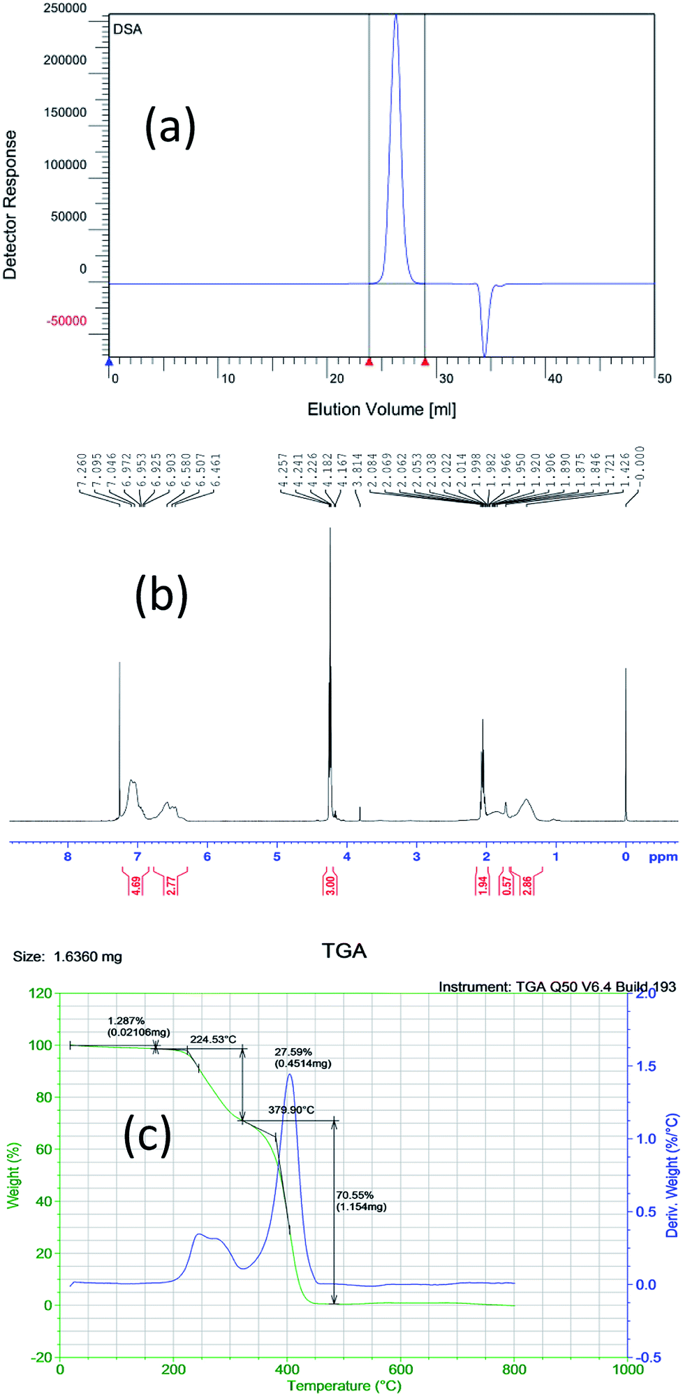 | ||
| Fig. 1 Different characterization results of the new BCP (PS-b-PC) based on (a) GPC, (b) NMR and (c) TGA. | ||
Previous investigation shows that ordered phase separation can be easily realized if the PS content in a diblock copolymer (PS-b-X) is controlled in the range of 53–72%. Beyond that range, more defects will be observed in self-assembled patterns, and even, to some extent, the phase separation will disappear completely.35–38 The molar content of PS in our diblock copolymer is 67%, which is consistent with the study above. The molecular structure of our diblock copolymer is sketched in Fig. 2. An important component in the structure is the –NH– group which can bond with Si–OH group on Si substrate to form a hydrogen bond, which plays an important role in contributing to vertical phase separation. More details will be discussed later.
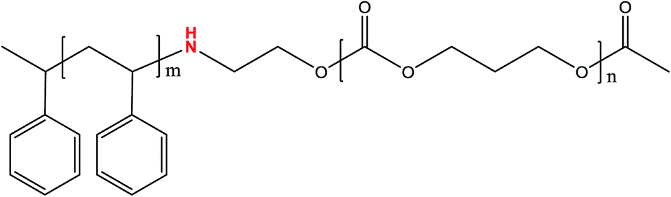 | ||
| Fig. 2 Chemical structure of PS-b-PC. | ||
Recent studies show that a practical approach to the design of high-χ BCPs is to increase either the hydrophobicity of the hydrophobic block or the hydrophilicity of the hydrophilic block in an amphiphilic BCP. As is well accepted, the relationship among the phase separation period (L0), Flory–Huggins parameter (χ), and the copolymer's degree of polymerization (N) can be expressed as L0 ≈ χ1/6N2/3.39 Since our PS-b-PC material has a very similar molecular structure to that of the material applied in the IBM paper, a value of χ of 0.19 from the IBM paper is suitable for our approximation calculation.40 The copolymer's degree of polymerization (N) is calculated as 60 as a result. L0 is calculated as 16.5 nm, which is very consistent with our experimental results. Specific parameters are listed in Table 3.
| Name | PS content (mol%) | PC content (mol%) | Molecular weight Mn | Nuclear magnetic resonance Mn | Glass transition temperature Tg | PDI |
|---|---|---|---|---|---|---|
| PS-b-PC | 67 | 33 | 7000 | PS(3.9k)-b-PC(2.0k) | 50.8 | 1.1 |
3.2 The micro-phase separation mechanism of PS-b-PC
After spin-coating PS-b-PC on the surface of the silicon substrate, the polymer constituting the diblock copolymer can be thermally annealed at above the glass transition temperature of the polymer. In the process of self-assembly, atoms, molecules, particles, and other constructions are driven by the system free energy, and at the same time, the micro-phase separation spontaneously occurs and they assemble themselves into periodic structures or special functional structures. In order to verify whether the phase separation forms lamellae oriented perpendicular to the substrate, a water contact angle experiment on a silicon substrate is carried out, as shown in Fig. 3. It is clearly observed that the surface energy of PS and PC is 50.17 mN m−1 and 49.12 mN m−1, respectively. The ratio is approximately 1:1 indicating vertically oriented lamellae on the substrate, as shown in Fig. 3.
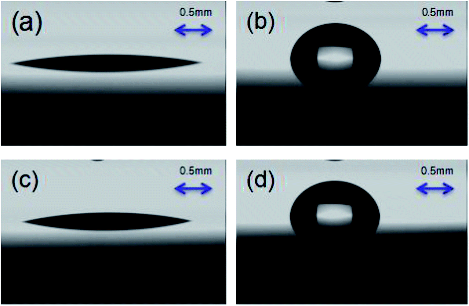 | ||
| Fig. 3 (a) The PS diiodomethane contact angle is 15.8°. (b) The PS water contact angle is 88.6°. (c) The PC diiodomethane contact angle is 17.2°. (d) The PC water contact angle is 86.8°. | ||
The PS-b-PC copolymer is dissolved in PGMEA with 1% solid content. The PS-b-PC solution is spin-coated on clean Si wafers with two spin speeds. The spin speed is set at 500 rpm for 5 s, and then quickly increased to 1000 rpm for 30 s. The film thickness is measured as about 35.2 nm by scanning electron microscopy (SEM) before annealing, as shown in Fig. 4(a). The substrates together with PS-b-PC films are baked in vacuum at different temperatures ranging from 140 to 190 °C for 10 min. SEM images show that vertical micro-phase separation is obtained for an annealing temperature at 160–170 °C for 10 min, as shown in Fig. 4(b) and (c). During the thermal annealing process, the mutual movement of block domains of BCP is promoted due to the existence of different surface energies for the two segments of BCP, leading to the system being more densely arranged. The film thickness after the bake is about 28.0 nm, a reduction of about 20.5%, as shown in Fig. 4(d).
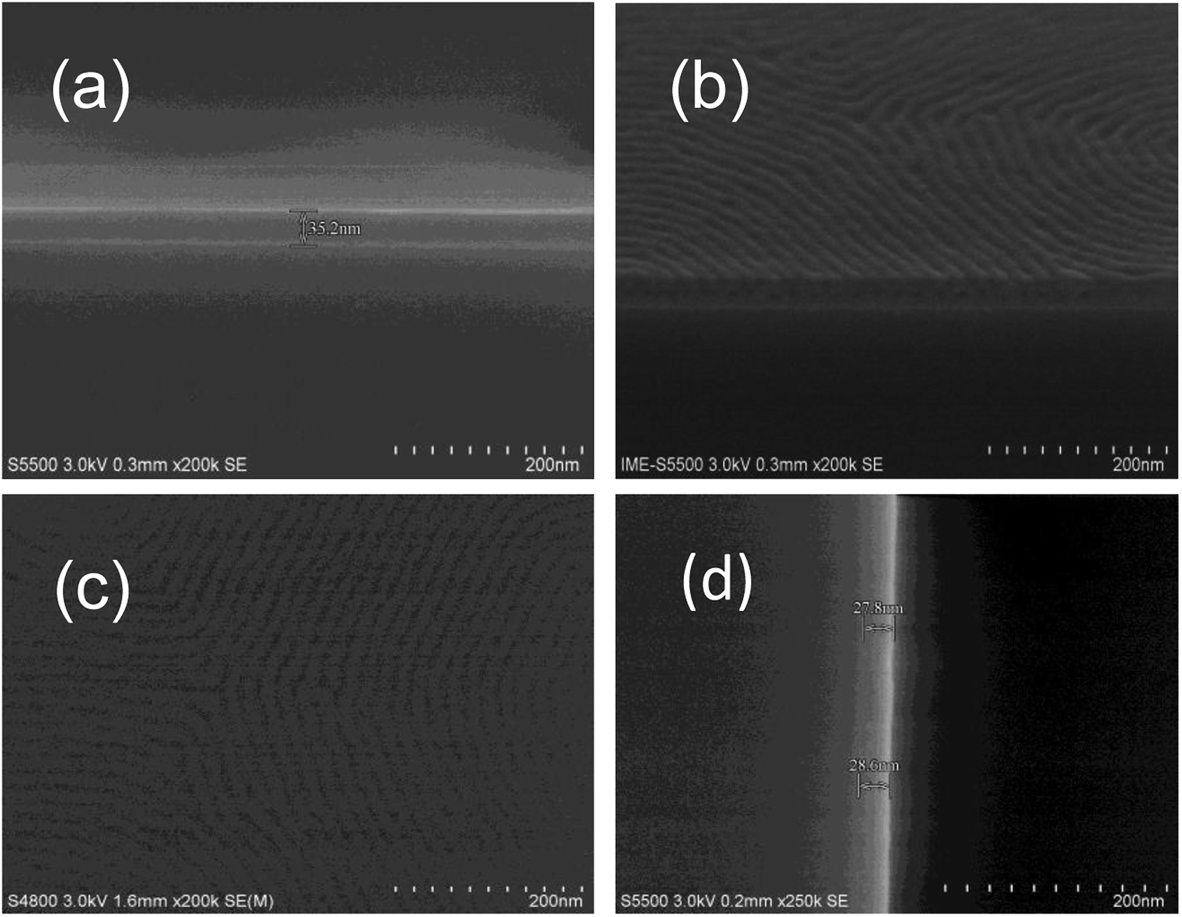 | ||
| Fig. 4 (a) Cross-sectional SEM image of PS-b-PC before annealing. (b) Cross-sectional and (c) top-down SEM images of PS-b-PC with no neutral layer. (d) Cross-sectional SEM image of PS-b-PC after annealing. | ||
The phase separation of the new BCP is very clear, as shown in Fig. 4(c). To know more about the local structural information obtained from SEM, grazing incidence small-angle X-ray scattering (GISAXS) is used to globally probe over large sample area and the entire film depth. The first peak of the first representation is not useful; the second peak is the highest and useful; the third peak is very small and useful. Sharp diffraction peaks of the second and third position at qy = 0.03738 Å−1 and qy = 0.0749 Å−1 (Fig. 5(a) and (b)) indicate a fully perpendicular lamella-forming structure well corresponding to a phase period of L0 = 16.8 nm, which is consistent with the SEM observations. Both SEM (Fig. 4) and GISAXS (Fig. 5) indicate that the micro-phase separation period is 16.8 nm with a good consistency between experiment and characterization.
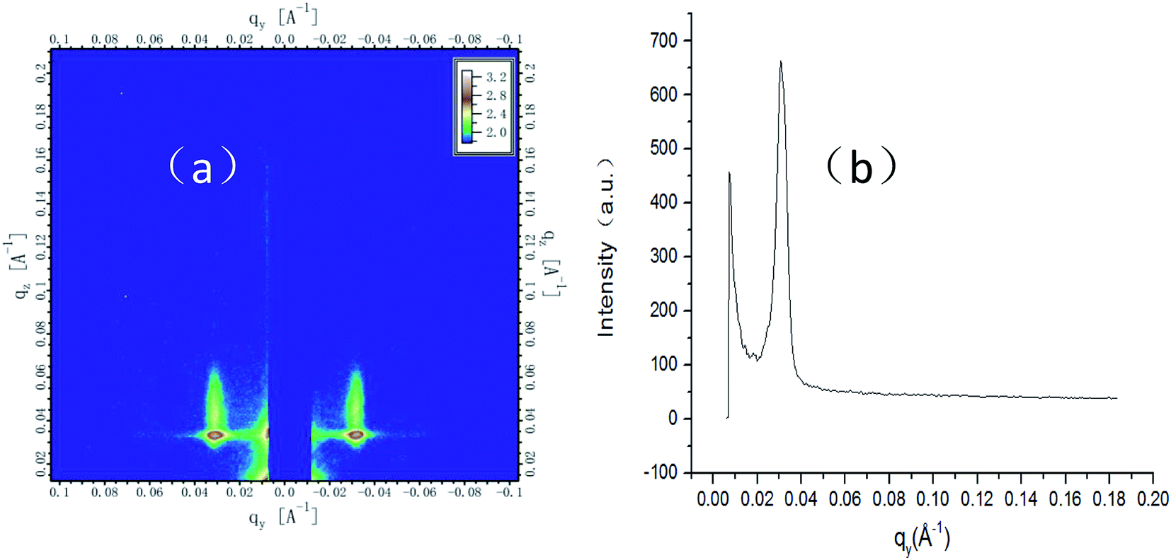 | ||
| Fig. 5 (a) GISAXS pattern of PS-b-PC. (b) GISAXS pattern of a bulk sample of PS-b-PC. A vertical layered microstructure of the sample is obtained and the second peak of qy is 0.03718 Å−1 for the thin film, and its phase period is 16.8 nm. | ||
As discussed above, PS-b-PC can easily form a vertical phase separation structure on the silicon substrate in the absence of a neutral layer. It is believed that hydrogen bonds formed by active H in the molecular structure binding with Si–OH on the silicon surface (NH⋯OH) may play an important role.42,43 The scheme of Si–OH formation on the silicon substrate surface and a simplified molecular structure of the BCP (PS-b-PC) are shown in Fig. 6(a) and (b), respectively. The copolymer (PS-b-PC) reacts with the silicon hydroxyl (–OH) groups on the silicon substrate to form hydrogen bonds which greatly contribute to the formation of a vertical micro-phase separation structure, as shown in Fig. 6(c). A schematic diagram of the hydrogen bonding mechanism is shown in Fig. 6(d). More details will be discussed later.
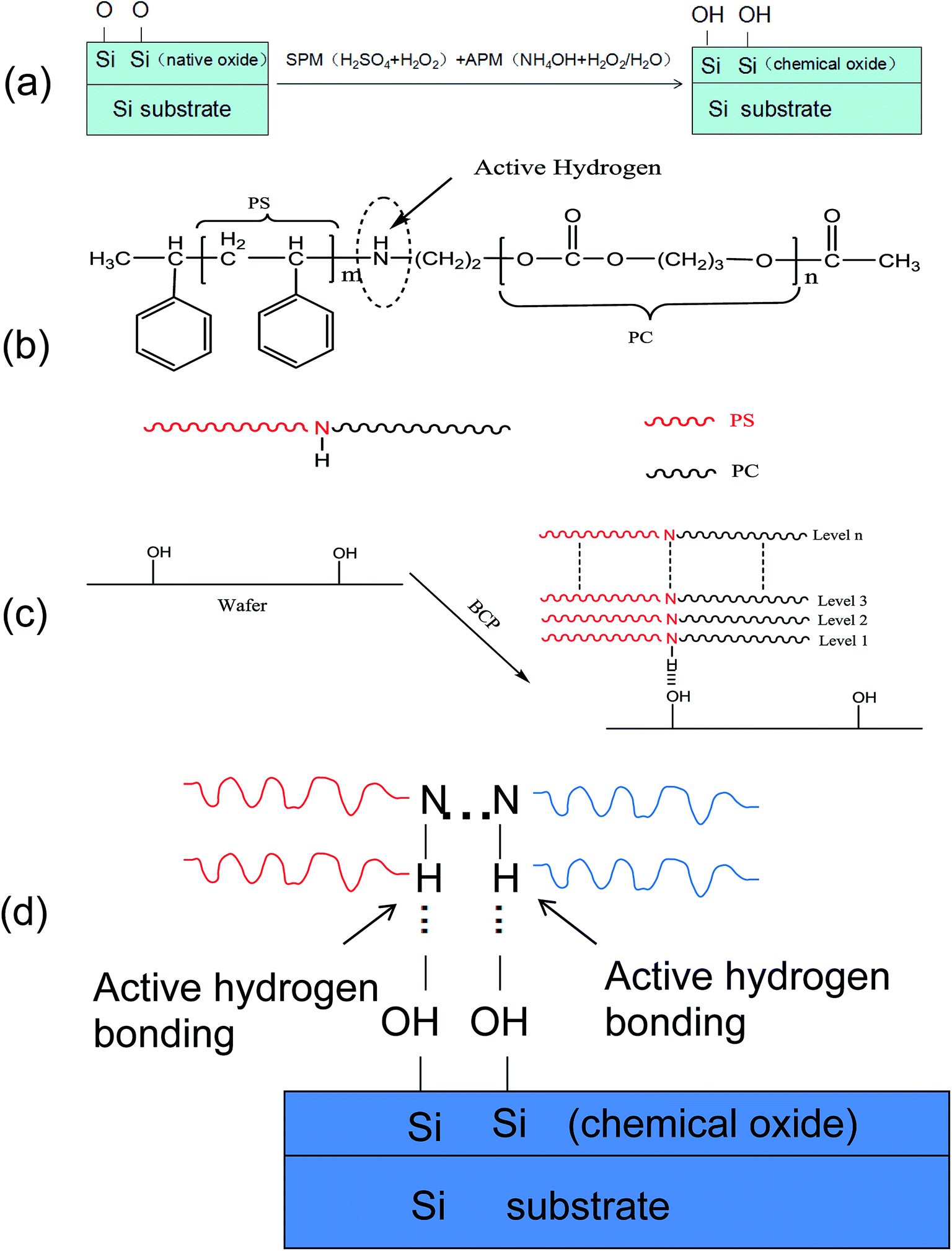 | ||
| Fig. 6 (a) Si–OH bonds are formed on the surface of the silicon substrate by appropriate wet cleaning treatment. (b) Molecular structure of the novel BCP (PS-b-PC). (c) An illustration of vertical micro-phase separation structure formation by hydrogen bonding. (d) A schematic diagram of the formation mechanism of hydrogen bonds. | ||
3.3 The formation mechanism of hydrogen bonds
As shown above, it is strongly believed that the active H plays an important role in promoting micro-phase separation of vertical structure in this work. To verify the assumption, a systematic experiment has been carried out by adding an epoxy-containing small monomer, n-butyl acrylate glycidyl ether, to the solution. It will react with the active H to form an alkyl-substituted hydroxyl group and block the active H, as shown in Fig. 7.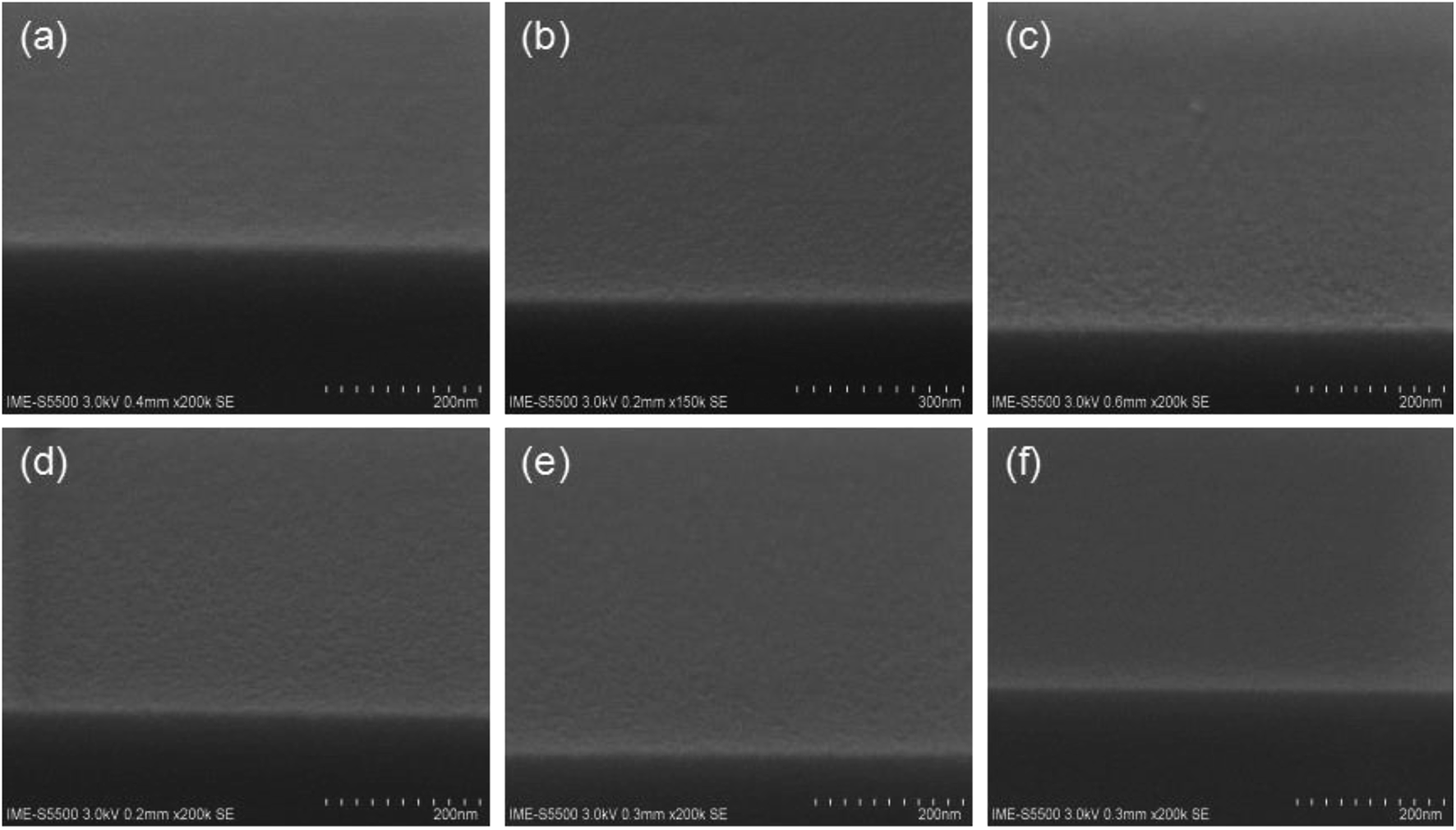 | ||
| Fig. 7 SEM images of PS-b-PC mixed with n-butyl acrylate glycidyl ether after annealing and with corresponding mixing ratios of (a) 3:1, (b) 2:1, (c) 1:1, (d) 1:2, (e) 1:3 and (f) 1:5. | ||
In the experiment, the volume ratio of PS-b-PC to n-butyl acrylate glycidyl ether (C7H14O2) ranges from 3:1, 2:1, 1:1, 1:2, 1:3 to 1:5. The mixture is firstly heated at 50 °C for 40 min, and then placed at room temperature for 10 hours for sufficient chemical reaction. In order to exclude the influence of over-dilution on PS-b-PC disable micro-phase separation, undiluted n-butyl acrylate glycidyl ether is added directly to the copolymer (PS-b-PC). The experiment shows that no visible phase separation structure can be observed, even if changing the mixing rate, as shown in Fig. 7.
Hexamethyldisilazane (HMDS) treatment is a common practice to change the hydrophobicity of Si substrate surface. After HMDS treatment, Si–OH on the surface becomes 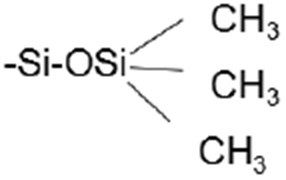 , achieving a successful transition from hydrophilic to hydrophobic. Accordingly, the water contact angle is changed from 15.4° to 79.2°, and no vertical micro-phase separation can be observed, which could be attributed to lack of polar hydrogen bonds on the silicon surface after treatment.
In most cases, the X–H bond is much stronger than the H⋯A bond (i.e. the N–H bond in this work is much stronger than the H⋯A bond). However, this does not mean that the two have no effect on each other. In fact, not only do they affect each other, but other atoms or groups connected to X and A also will exert an influence. It is important to point out that a strong polar group 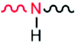 at the junction of two blocks of PS and PC is introduced intentionally in this work. The N–H bond (donor) in the novel BCP (PS-b-PC) interacts with the Si–OH bond on the silicon substrate to form a hydrogen bond anchored on the silicon substrate.
The hydrogen atoms that form hydrogen bonds must have a partial positive charge, while the hydrogen bond acceptor can be an atom, anion, molecular fragment, or molecule, as long as it has a region with high electrical charge. When the silicon substrate is cleaned in SPM + APM solution, silanol groups are easily formed on the substrate. Once PS-b-PC is spin-coated on the substrate, hydrogen bonds (N–H⋯OH) will be formed between the active N–H bond and the Si–OH bond by an appropriate annealing process. It is especially worth noting that a hydrogen bond is a unique non-covalent bonding phenomenon, with a certain degree of directionality and strength. Moreover, its formation is highly reversible and reproducible, and the process is also fast. In macromolecular chemistry, hydrogen bonds can control and direct the structure of molecular aggregates in the entire structure as well as some local specific sites. The directionality gives rise to selectivity and specificity to the intermolecular recognition process. For our new BCP, since the surface energies of the PS and PC blocks are almost identical, the preferential adsorption of a certain block on the substrate is unlikely. Instead, the two blocks can reach a delicate balance on the substrate. Under the influence of the hydrogen bond (N–H⋯OH) vertical lamella-forming structures can be successfully achieved in the absence of a neutral layer.
All in all, the combination of theory and experimental verification proves that the hydrogen bond is a real driving force in contributing to the formation of a periodic and lamella-forming phase separation structure, with the domains oriented perpendicular to the substrate in the absence of neutral layer by means of our specifically developed BCP material.
It is especially worthwhile noting that the schematic hydrogen bonding mechanism proposed here is a little like an uppercase letter “V”, as shown in Fig. 8. For this reason, the hydrogen bond mechanism is also called the “V” model. Both ends of the “V” are PS and PC blocks at the left and right, and its bottom end is the hydrogen bond formed between silanol and –NH–. And then, layer by layer, the perpendicular micro-phase separation structures is formed on the silicon substrate.
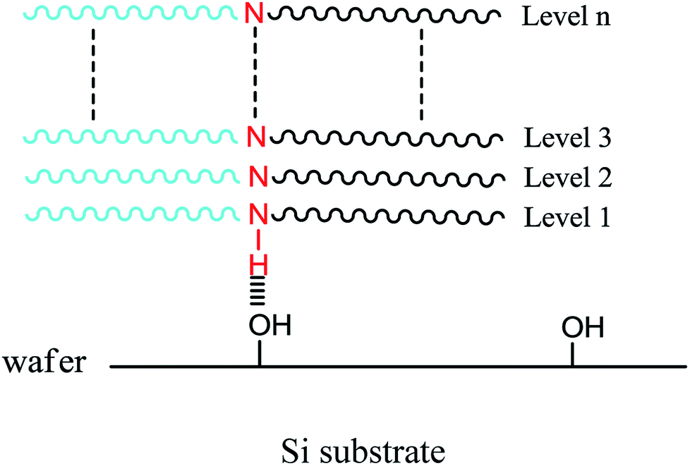 | ||
| Fig. 8 A schematic diagram of the “V” model forming a periodic and lamella-forming phase separation structure perpendicular to the substrate without a neutral layer. | ||
3.4 Application of new PS-b-PC on different substrates
As discussed above, the hydrogen bond (N–H⋯OH) plays an important role in promoting the vertical phase separation of PS-b-PC on silicon substrates. Besides silicon substrate, the novel PS-b-PC copolymer was also used with some silicon-based substrate materials such as SiO2 and Si3N4. Here, a few simple experiments are provided as a reference. We have investigated four different film stacks on Si substrates with no neutral layer, using annealing temperatures of each of 160 and 170 °C. The four different types of film stacks are as follows: (1) 40 nm thick SiO2; (2) 40 nm thick Si3N4; (3) 40 nm thick SiO2 + 30 nm thick Si3N4; (4) 40 nm thick Si3N4 + 30 nm thick SiO2. After film deposition followed by wet cleaning in SPM and APM solutions, –OH bonds will easily form on the surface.44–46 At the same time, PS-b-PC is spin-coated on the substrates directly without any extra process. Under the process conditions, the Si–OH bond on the surface of SiO2 and Si3N4 combines with the –NH– bond in the novel BCP to form a hydrogen bond, which promotes vertical phase separation, as shown in Fig. 9.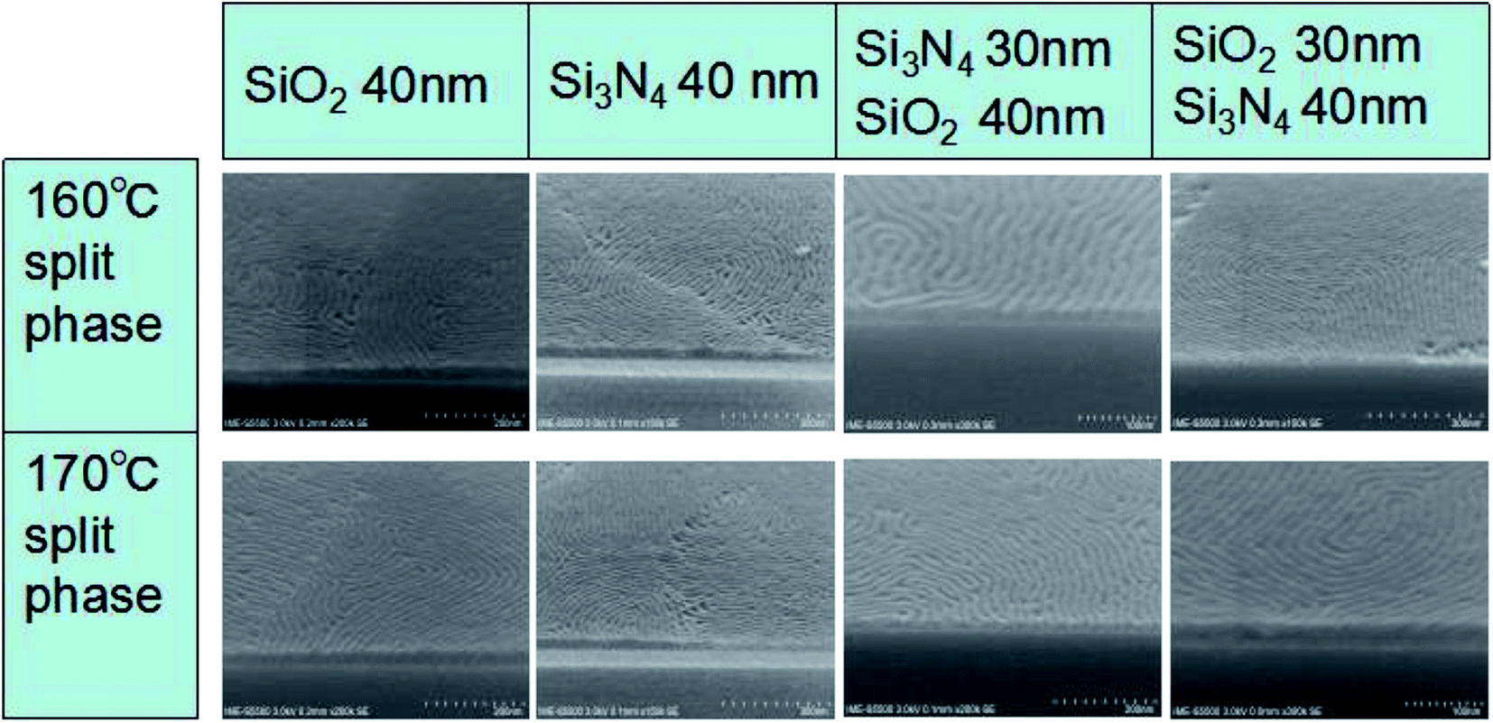 | ||
| Fig. 9 SEM images of PS-b-PC on four different substrates after annealing at 160 °C and 170 °C. | ||
Since the present paper focuses on an investigation of micro-phase separation mechanism in the absence of a neutral layer, a detailed pattern transfer into the underlying substrate to achieve specifically designed structures is well beyond the intended scope of this work. Some related work on pattern transfer was reported in our previously published paper regarding advanced CMOS devices.47,48 Currently, a DSA-related study with no neutral layer is being carried out in different design layout trenches to achieve sub-20 nm features with a long-range order, and interesting results will be further published in following papers.
4. Conclusions
A novel high-χ diblock copolymer (PS-b-PC) has been synthesized by our innovative customization. Vertical micro-phase separation with a pitch of 16.8 nm can be successfully achieved using only thermal annealing and a spin-coating process without any neutral layer on a Si substrate, which makes PS-b-PC a promising candidate for next-generation lithography. The result is mainly attributed to the hydrogen bond formed by the interaction of silanol with the active H in the –NH– group. Also, the novel PS-b-PC can be successfully applied on some other silicon-based substrates, such as SiO2 and Si3N4, to fabricate various periodical nanostructures or functional electronic devices. The innovatively developed BCP material greatly reduces the complexity of process conditions and manufacturing costs, and is suitable for delivering large-area patterning for advanced nanofabrication. We believe that PS-b-PC has an extremely important application value in the semiconductor industry. Simultaneously, the scope of future work will be focused on further optimization in reducing domain spacing, line edge/width roughness and process time, as well as the pattern transfer process for this kind of BCP on more interfaces of substrates.Conflicts of interest
There are no conflicts to declare.Acknowledgements
This work was supported by the National Science and Technology Major Project of China (2017ZX02315001-003), the Sichuan Provincial Science and Technology Program (2018G20321), the National Natural Science Foundation of China (NSFC) (61804174, 61604172), the Guizhou Province Science and Technology Talents (20185616), and the National Natural Science Foundation of China (NSFC) (61741505, 61865002). The authors thank the Integrated Circuits Advanced Process Center in the Institute of Microelectronics of Chinese Academy of Sciences (IMEICAS), and Jiangsu HanTop Photo-Materials Co. Ltd.References
- C. K. Jeong, H. M. Jin, J. H. Ahn, T. J. Park and H. G. Yoo, Small, 2014, 10, 337–343 CrossRef CAS PubMed
.
- A. Checco, A. Rahman and C. T. Black, Adv. Mater., 2014, 26, 886–891 CrossRef CAS PubMed
- L. Meng, X. He, J. Gao, J. li and Y. Wei, Nanotechnology, 2015, 26, 415303 CrossRef PubMed
- L. Meng, X. He, J. Gao, J. li and Y. Wei, Nanoscale Res. Lett., 2016, 11, 505 CrossRef PubMed
- H. Tsai, J. W. Pitera, H. Miyazoe, S. Bangsaruntip, S. U. Engelmann and C. C. Liu, ACS Nano, 2014, 8, 5227–5232 CrossRef CAS PubMed
- H. Yi, X. Y. Bao, R. Tiberio and H. S. Wong, Nano Lett., 2015, 15, 805 CrossRef CAS PubMed
- C. Cummins, D. Borah, S. Rasappa, R. Senthamaraikannan, C. Simao and A. Francone, ACS Omega, 2017, 2, 4417–4423 CrossRef CAS
- S. M. Park, X. Liang, B. D. Harteneck, T. E. Pick, N. Hiroshiba and Y. Wu, ACS Nano, 2011, 5, 8523–8531 CrossRef CAS PubMed
- C.-C. Liu, F. L. Lie, V. Rastogi, E. Franke, N. Mohanty, R. Farrell, H. Tsai, K. Lai, M. Ozlem, W. Cho, S. G. Jung, J. Strane, M. somervell, S. Burns, N. Felix, M. Guillorn, D. Hetzer, A. Ko and M. Colburn, Proc. SPIE, 2016, 9423, 94230S Search PubMed
- H. Y. Tsai, H. Miyazoe, J. Cheng, M. Brink, S. Dawes, D. Klaus, J. Buccignano, D. Sanders, E. Joseph, M. Colburn and M. Guillorn, Proc. SPIE, 2015, 9423, 942314 CrossRef
- H. Kato, Y. Seino, H. Yonemitsu, H. Sato, M. Kanno, K. Kobayashi, A. Kawwanishi, T. Imamura, M. Omura, N. Nakamura and T. Azuma, J. Photopolym. Sci. Technol., 2013, 26, 21–26 CrossRef CAS
- M. Argoud, I. Servin, A. Gharbi, P. P. Barros, K. Jullian, M. Sanche, G. C. Maitral, S. Barnola, R. Tiron, C. Navarro, X. Chevalier, C. Nicolet, G. Fleury, G. Hadziioannou, M. Asai and C. Pieczulewski, Proc. SPIE, 2014, 9049, 904929 CrossRef
- F. S. Bates and G. H. Fredrickson, Annu. Rev. Phys. Chem., 1990, 41, 525–557 CrossRef CAS PubMed
- S. Kim, D. O. Shin, D. G. Choi, J. R. Jeong, J. H. Mun, Y. B. Yang, J. U. Kim, S. O. Kim and J. H. Jeong, Small, 2012, 8, 1563–1569 CrossRef CAS PubMed
- S.-J. Jeong, H.-S. Moon, J. Shin, B. H. Kim, D. O. Shin, J. Y. Kim, Y.-H. Lee, J. U. Kim and S. O. Kim, Nano Lett., 2010, 10, 3500–3505 CrossRef CAS PubMed
- C. T. Black and O. Bezencenet, IEEE Trans. Nanotechnol., 2004, 3, 412–415 CrossRef
- Y.-H. La, E. W. Edwards, S.-H. Park and P. F. Nealey, Nano Lett., 2005, 5, 1379–1384 CrossRef CAS PubMed
- E. Han, K. O. Stuen, M. Leolukman, C.-C. liu, P. F. Nealey and P. Gopalan, Macromolecules, 2009, 42, 4896–4901 CrossRef CAS
- H. S. Suh, H. Kang, P. F. Nealey and K. Char, Macromolecules, 2010, 43, 4744–4751 CrossRef CAS
- C.-C. Liu, P. F. Nealey, A. K. Raub, P. J. Hakeem, S. R. L. Brueck, E. Han and P. Gopalan, J. Vac. Sci. Technol., B: Microelectron. Nanometer Struct.--Process., Meas., Phenom., 2010, 28, C6B30 CrossRef CAS
- M. Russel, Science, 1994, 265, 612–614 CrossRef CAS PubMed
- M. Russel, J. Mol. Biol., 1998, 279, 485–499 CrossRef CAS PubMed
- M. Russel, Mol. Microbiol., 2010, 5, 1607–1613 CrossRef
- M. Husemann, D. Mecerreyes, C. J. Hawker and J. L. Hedrick, Angew. Chem., Int. Ed., 1999, 38, 647–649 CrossRef CAS PubMed
- Z. Merican, T. L. Schiller, C. J. Hawker, P. M. Fredericks and I. Blakey, Langmuir, 2007, 23, 10539 CrossRef CAS PubMed
- Y. Kim, J. Pyun, J. M. Fréchet, C. J. Hawker and C. W. Frank, Langmuir, 2005, 21, 10444–10458 CrossRef CAS PubMed
- I. In, Y. H. La, S. M. Park, P. F. Nealey and P. Gopalan, Macromolecules, 2008, 41, 9090–9097 CrossRef
- E. Han, K. O. Stuen, Y.-H. La, P. F. Nealey and P. Gopalan, Macromolecules, 2008, 41, 9090–9097 CrossRef CAS
- E. Han and P. Gopalan, Langmuir, 2010, 26, 1311–1315 CrossRef CAS PubMed
- B. E. Han, I. In, S.-M. Park, Y.-H. La, Y. Wang, P. F. Nealey and P. Gopalan, Adv. Mater., 2007, 19, 4448–4452 CrossRef
- M. Q. Li, K. Douki, K. Goto, X. F. Li, C. Coenjarts, D. M. Smilgies and C. K. Ober, Chem. Mater., 2004, 16, 3800–3808 CrossRef CAS
- E. Han and P. Gopalan, Langmuir, 2010, 26, 1311–1315 CrossRef CAS PubMed
- A. Vora, A. Chunder, M. Tjio, S. Balakrishman, E. Lofano, J. Cheng, D. P. Sanders, E. Hirahara, Y. Akiyama, O. Polishchuk, M. Paunescu, D. Baskaran, S. E. Hong and G. Lin, J. Photopolym. Sci. Technol., 2014, 27, 419–424 CrossRef
- A. Vora, A. Chunder, M. Tjio, T. Magbitang, E. Lofano, N. Arellano, K. Schmidt, K. Nguyen, J. Cheng and D. P. Sanders, J. Photopolym. Sci. Technol., 2015, 28, 659–662 CrossRef CAS
- E. Han, K. O. Stuen, Y.-H. La, P. F. Nealey and P. Gopalan, Macromolecules, 2008, 41, 9090–9097 CrossRef CAS
- E. Han and P. Gopalan, Langmuir, 2010, 26, 1311–1315 CrossRef CAS PubMed
- D. Y. Ryu, J.-Y. Wang, K. A. Lavery, E. Drockenmuller, S. K. Satija, C. J. Hawker and T. P. Russell, Macromolecules, 2007, 40, 4296–4300 CrossRef CAS
- E. Han, K. O. Stuen, M. Leolukman, C.-C. Liu, P. F. Nealey and P. Gopalan, Macromolecules, 2009, 42, 4896–4901 CrossRef CAS
- G.-W. Yang, G.-P. Wu, X. X. Chen, S. S. Xiong, C. G. Arges, S. G. Ji, P. F. Nealey, X.-B. Lu, D. J. Darensbourg and Z.-K. XU, Nano Lett., 2017, 2, 1233–1239 CrossRef PubMed
- A. Vora, E. Hirahara, J. Cheng, D. Baskaran and O. Polishchuk, US Pat. US20160244557[P], 2016
- E. B. Gowd, M. S. Rama and M. Stamm, Nanostructures based on self-assembly of block copolymers, Springer, 2012 Search PubMed
- H. Zeng, R. S. Miller, R. A. Flowers and B. Gong, J. Am. Chem. Soc., 2000, 122, 2635–2644 CrossRef CAS
- M. Li, K. Yamato, J. S. Ferguson, K. K. Singarapu, T. Szyperski and B. Gong, J. Am. Chem. Soc., 2008, 130, 491 CrossRef CAS PubMed
- T. A. Dang and R. Gnanasekaran, J. Vac. Sci. Technol., A, 1991, 9, 1406–1409 CrossRef CAS
- F. Milanesi, S. Vendrame, E. Spadoni, F. Pipia and L. Livellara, Solid State Phenom., 2015, 219, 36–39 Search PubMed
- J. Haisma, G. A. C. M. Spierings, T. M. Michielsen and C. L. Adema, Philips J. Res., 1995, 49, 23–46 CrossRef CAS
- L. Meng, P. Hong and X. He, Appl. Surf. Sci., 2016, 362, 483–489 CrossRef CAS
- L. Meng and J. Yan, ECS J. Solid State Sci. Technol., 2017, 6, 23–28 CrossRef
| This journal is © The Royal Society of Chemistry 2019 |