
 Open Access Article
 This Open Access Article is licensed under a Creative Commons Attribution-Non Commercial 3.0 Unported Licence
First-principles analysis for the modulation of energy band gap and optical characteristics in HgTe/CdTe superlattices
A. Laref *ab,
M. Alsagria,
Z. A. Alahmeda and
S. Larefc
*ab,
M. Alsagria,
Z. A. Alahmeda and
S. Larefc
aDepartment of Physics and Astronomy, College of Science, King Saud University, Riyadh, 11451 King Saudi Arabia. E-mail: amel_la06@yahoo.fr; Fax: +886 2 33665136; Tel: +886 2 33665156
bDepartment of Physics, National Taiwan University, Taipei 106, Taiwan
cFachbereich Chemie, Philipps-Universität Marburg, Hans-Meerwein-Str., D-35032 Marburg, Germany
First published on 24th May 2019
Abstract
HgTe/CdTe superlattices (SLs), have emerged as unprecedented materials with tremendous functionalities, such as solar photocell devices. We carried out first-principles analyses in the framework of the full-potential linearized augmented plane wave (FP-LAPW) scheme to understand the impact of layer periodicity and strain on HgTe/CdTe superlattices. This technique allows us to describe the electronic and optical features of low dimensional systems, such as CdTe–HgTe heterojunctions. Alteration of the layer thickness and strain is imperative for tailoring the energy band gap of HgTe/CdTe superlattices. Thus, the CdTe and HgTe layers possess an appreciable influence on the induced forbidden gap of SLs because of their distinct quantum confinement characteristics. The electronic structures illustrate that the alteration in HgTe and CdTe layer thickness is pivotal for the overlap or non-overlap of the conduction bands and valence bands. Indeed, these systems can yield a semi-metallic or normal state with significant modification in the optical absorption of HgTe/CdTe SLs with respect to their bulk counterparts. Such SL systems have several advantageous features, involving their tailorable near band edge optical properties. Hence, it is feasible to optimize the requisite characteristics for electronic devices based on these SLs. This may enhance the development of HgTe/CdTe SLs in vast applications envisioned in infrared devices.
Introduction
Recent advances in semiconductor film technology have enhanced the applicability of group II–VI compounds in diverse arenas, such as light emitters at normal conditions, blue laser fabrication techniques, optical switching devices, optical wave guides, high density optical memories, and modulated heterostructures.1–6 The evolution of thin film solar cells serves as a compelling realm of scrutiny. Much consideration has been dedicated to the progress of high efficiency and low price thin film solar cells. In this respect, CdTe exemplifies as pertinent classes for manufacturing thin film solar cells because of its optimal forbidden gap, and large absorption coefficient. Seminal papers have reported that this interesting system is a promising photovoltaic material for next generation photovoltaic cells, in the form of tandem cells and nanostructured cells.3–15 A technological breakthrough was achieved by the incorporation of CdTe thin film in low-dimensional heterostructures, such as multiple quantum wells (MQWs) and quantum dots (QDs). Over the past half-century, major advances and breakthroughs related to Mercury Cadmium Telluride (MCT) semiconductors have taken place. These ternary semiconducting alloys possess a direct energy gap with a band gap energy spanning from 1.5 eV for binary CdTe to −0.3 eV for binary HgTe. Its adjustable band gap energy covers nearly the entire infrared spectrum.16–30 It is well known that the quantum confinements in artificial, low-dimensional semiconductor structures strongly modify the electronic properties,10–15 which play a prominent role in the performance of optoelectronic devices.3–8 The prior experimental and theoretical investigations have been mainly concentrated on type-I9,15 or type-II SLs30 that are made up of direct band gap or indirect band gap semiconductors. A survey of the literature indicates that SLs based on II–VI compounds and their alloys aroused a tremendous interest, when compared to the SLs involving group IV and III–VI semiconductors.19,30 They are deemed to appertain to a class of type-III SLs, owing the unique merged zero energy gap semiconductor, HgTe and a positive direct energy gap semiconductor, CdTe. Impressively, the design of semiconducting QWs and SLs can be established from the alternated layers of CdTe semiconductor and semi-metallic HgTe semiconductor. The composition of the QW devices elicits novel properties from the heterostructures consisting of alternating ultrathin layers of two semiconductors with different band gaps.Due to the inherent control over their properties, HgTe/CdTe SLs, which consist of a semimetal and semiconductor, are considered as attractive systems for various applications. Due to the cubic crystal structure (zinc-blende (ZB)) of CdTe and HgTe compounds, as well as the offset value between the valence band edges, these SLs have gained salient characteristics. The small lattice mismatch between HgTe and CdTe allows for relatively high quality epitaxial heterostructures. Accordingly, for holes and electrons, the barriers and wells are comprised by CdTe-layer and HgTe-layers, respectively. As the electronic and optical properties are strongly dependent on the well and barrier thickness, the interdiffusion processes are expected to lead to appreciable effects on the electron–hole sub-bands. However, the fabrication of good quality heterostructures with abrupt interfaces is especially entailed for more advanced devices. Based on experimental techniques such as molecular beam epitaxy, the growth of HgTe/CdTe SLs with good crystalline quality can be achieved. The study of SLs accomplished on alternating layers of two semiconductors has also been a fruitful source of new realization on interfaces, band structures, induced band gap, and novel quantum effects on a submicron scale. These materials can be applied in high-performance IR detectors, primarily owing to the band gap modulation capability, unlike in other IR detector materials, such as extrinsic silicon photoconductors.23–31 For this reason, the telluride is imputed as a strong rival relatively to III–V materials in the optoelectronic device market.
From the prior experimental measurements, it was pointed out that the sub-band structures of these striking SLs have been inspected by means of resonant light-scattering technique. Controlling the thickness of the HgTe and CdTe layers can aid tailor the band energy to the required value, from zero to a few hundred meV (covering the whole 3–12 μm spectrum region).20–26 In addition, novel electronic effects can be produced due to the quantum confinement in relatively large scale structures fabricated using Hg-based materials. Furthermore, the band gap of the SL can be tailored by incorporating a strain impact of the layers. Theoretical efforts also predicted an occurrence of inversion in the band alignment of an HgTe layer thicker than 6.3 nm,29–49 and thereby this behavior was proved to be ideal for the observation of a quantum spin Hall insulator phase.32–37,41–45 The HgTe/CdTe QW exhibited a quantum phase transition where the electronic structure changes from normal to invert state. In this regard, HgTe–CdTe semiconductors are once again under the spotlight now, owing to the topological insulating (TI) behavior of HgTe system. It has been proven that the HgTe monolayer undergoes a transition from a topologically trivial phase to a topologically nontrivial phase as the in-plane tensile strain ε increases beyond 2.4%.13,14,21,22 However, the strain induced TI behavior was due to the combination effects of strain and spin–orbit coupling (SOC). The large band gap tunability of 2D HgTe renders it a suitable material for practical applications in spintronics and quantum computing at room-temperature.13,14,22,32–35,42–45
For prospective technological applications, it is imperative to catch the physical behaviors of the (HgTe)n/(CdTe)n SLs. For this purpose, realistic calculations are reported to analyze in detail the electronic structures, band parameters, and optical properties of unstrained and strained (HgTe)n/(CdTe)n (n = 2–4) SLs. The small mismatch between the CdTe and HgTe lattices can lead to highly crystallized heterostructure interfaces. These systems can be grown experimentally by avoiding misfit dislocations. In this regard, the state-of-the-art first-principles FP-LAPW scheme which is based on the density-functional theory (DFT),50 as implemented in the WIEN2K package,51,52 is employed to explore the nature of confinement in the unstrained and strained HgTe wells and their relationship to the barrier thickness, by incorporating the SOC effect. In order to yield a judiciously precise forbidden gap irrespective with the experimental results, we employ the recently elaborated, the modified Becke–Johnson (mBJ) exchange potential53 in conjunction with the generalized gradient approximation (GGA) correlation potential, namely mBJ-GGA approach. Therefore, these improved calculations are very practical for resolving the band gap issue and alignment of energy bands in HgTe/CdTe SLs as functions of the layer thickness, which has a tendency to change the related electronic structures. Another interesting result of the present theoretical investigation concerns the existence of two types of confinement characters for the interface states in the unstrained and strained HgTe/CdTe SLs. These novel prototypical nano-structures could manifest while inspecting the confinement impact on the electronic states of HgTe/CdTe SLs. For this purpose, we analyze the band structure and the density of states of the unstrained and strained structures of the SLs by altering the layer thickness. The compelling features of HgTe compound, the so-called SOC strength and band inversion had render it the appealing system in the topical inspection. The prominence of relativistic effects are inserted in this heavier element (Hg) due to their markedly impact on the splitting of the utmost valence states of the band structures of these SLs. This could conduct to the electron-like and heavy-hole-like states in the HgTe layer and the light-hole-like states in the CdTe layer being well confined.24–31,42–45,54–61 The fact is that the width of the band gap strongly depends on the hybridization of the interface states with the heavy-hole-like sub-bands. This implies that the interface states are significant for examining the optical properties, such as the optical absorption, of the HgTe/CdTe SLs. The absorption coefficients of the SLs are expected to be greater than those of HgCdTe alloys because of the large band-edge density of the states in the SL. This indicates that the SL absorber regimes in the detectors can be thinner, when compared with the traditional alloys. This would be of tremendous advantage in designing low-dimensional materials made of HgTe/CdTe based heterostructures with novel features for optoelectronic devices.
The present paper is structured as follows. Initially, the computational calculations will be presented. Then, the main results will be discussed, in terms of the variation of the semiconductor layers and strain impact on the band gap, density of states and optical characteristics of the HgTe/CdTe SLs. Finally, we present our conclusions and perspectives.
Computational method
Our theoretical simulations are accomplished by employing an all-electron FP-LAPW approach in the DFT framework as embodied in the WIEN2K package.51 In our calculations we employed relativistic FP-LAPW methodology, such that the SOC effects are undertaken in the scalar scheme. For exchange and correlation potential, the GGA of Perdew–Burke–Ernzerhof (PBE) functional is adopted52 in order to compute the total energy of all systems. In order to surmount the shortcomings of the underestimated GGA approach for the energy gap and band splitting, the mBJ-GGA + SOC technique is taken into account.53 The mBJ-GGA + SOC approach has proven its reliability to successfully simulate the energy gap, thus yielding a better band splitting.Our calculations are established using the total energy optimization with respect to the cell parameters, in order to acquire better results for the structural values of lattice constants (a and c) corresponding to the minimum energy of HgTe/CdTe SLs. The considered compounds adopt a ZB structure with a primitive cell of two atoms, such that the lattice constant varies from 6.453 Å for CdTe to 6.467 Å for HgTe. The computed lattice parameter of HgTe is 0.142% overestimated relatively to the experimental one (aHgTe(exp) = 6.460 Å), whereas for CdTe the lattice constant is 0.154% overestimated comparatively to the experimental one (aCdTe(exp) = 6.447 Å).33,62 The portrayal of the structures of the SLs is as follows. The SL is represented by an artificial structure encompasses alternated layers of two dissimilar semiconductor materials, constituting a periodic sequence of QWs and barriers. In other words, the arrangements of the alternated n layers of CdTe and HgTe are constructed along the growing (001) direction in the (HgTe)n/(CdTe)n SL. The minimized lattice parameter of CdTe which is referred as substrate allows the optimization of the in-plane lattice constant. The out-of-plane lattice parameter is acquired by the optimized averaged value of the lattice parameter between the bulk compounds CdTe and HgTe, for an ideal interface. The (001) direction is undertaken as the polar growth axis. A tetragonal symmetry (n is the number of CdTe and HgTe mono-layers) was handled for the SL(n, n) and the corresponding interfaces with periodic boundary conditions. VSL specifies n times the bulk volume, as the elementary cell. The unit translational vectors of the (HgTe)n/(CdTe)n superlattices [SL(n, n)] are represented as: a1 = a0/2(1, 1, 0), a2 = a0/2(−1, 1, 0), a3 = a0/2(0, 0, n) where the lattice constant is denoted by a0 and n × a0 specifies the periodicity of SL(n, n). A periodic supercell is constructed along the (001) direction (z-axis perpendicular to layers, as well as the x and y axes parallel to it) to catch the structure of these SLs with HgTe-layers and CdTe-layers. Note that the Te takes place the ZB anion atomic sites, while the mixture between Hg and Cd are occupied in ZB cation atomic sites, as depicted in Fig. 1. For the calculation of the unstrained SLs and those under biaxial tensile strain (4%), n is varied from 2 to 4, along with the optimized lattice parameters.
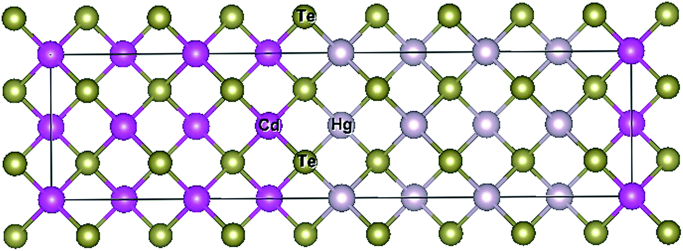 | ||
| Fig. 1 Contribution of interface illustrates the growth of HgTe and CdTe atoms over the (001) direction of the SLs. | ||
Results and discussion
Electronic structures of unstrained and strained (HgTe)n/(CdTe)n superlattices
For a deeper insight, we compute the electronic properties, more specifically the band structures and density of states (DOS) of unstrained and strained HgTe/CdTe SLs grown along the (001) direction using the mBJ-GGA + SOC approach. Note that the relativistic effects in terms of the SOC are relevant for representing the states of heavy elements, such as Hg. We start by representing the band structure results of the unstrained and strained of (HgTe)n/(CdTe)n SLs; the number of layers (n) was varied from 2 to 4. (n = 2–4) at the high symmetry k-points in the BZ, whilst the short periodicity of layers contains the alternative layers of CdTe and HgTe, as portrayed in Fig. 2(a1–a3) and (b1–b3). For all systems, the valence band maximum (VBM) is located at the Γ-point. Note that the zero Fermi level is situated at the VBM. The alteration in the energy gap is a result of the variation in the number of layers in the HgTe/CdTe SLs and the strain impact. It is noticeable that the representative energy dispersions exhibit an increased number of sub-bands for the VBM and conduction band minimum (CBM), when the layer thickness is increased. These SL systems with alternating CdTe and HgTe layers are constructed parallel to the (001) plane, although the z-axis, which represents the confinement direction, is normal to the heterostructure. Accordingly, the electronic energy band structures of these SLs are perpendicular to the growth direction, along the z direction, exhibiting zone folding (Fig. 2), when compared with the CdTe and HgTe bulk counterparts.26 Note that the electron is always confined within the CdTe slab; this is a result of the quantum confinement effect in such SLs. The electron confinements are positioned in the CdTe layers that represent the CB at Γ6, whereas the hole confinements in the HgTe layers describe the VB at Γ8. Clearly, the band structure profiles of the (HgTe)n/(CdTe)n SLs possess quite similar shapes, although the small difference in the SO splitting is proportional to the variation in the monolayer numbers of the two constituents in the SLs.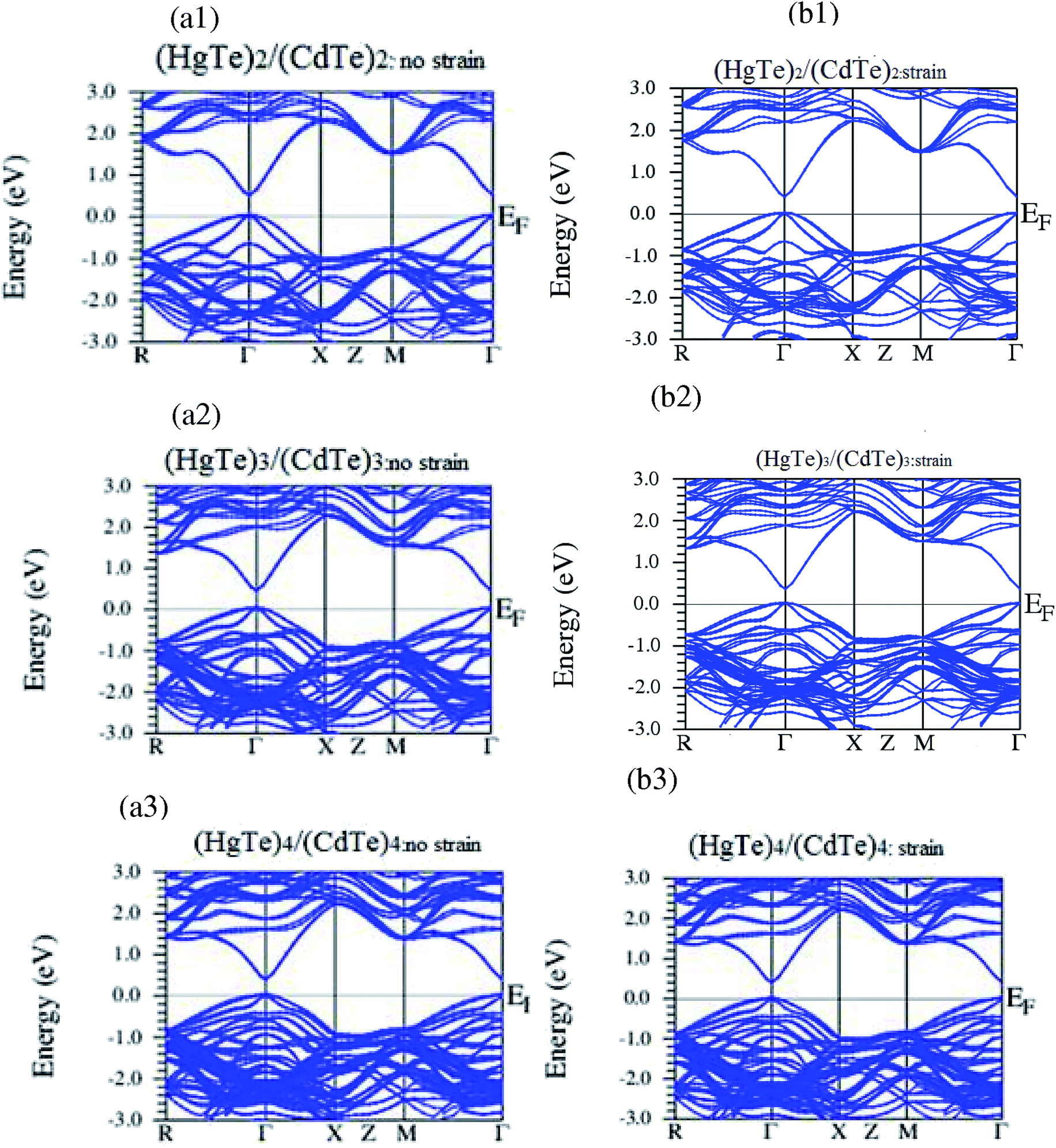 | ||
| Fig. 2 The band structures of (a1–a3) unstrained and (b1–b3) strained layers of (HgTe/CdTe)n superlattices (n = 2–4) grown over the (001) direction. | ||
It is clear that the semi-metallic nature of HgTe is characterized by a degeneracy near the Fermi level with two types of charge carriers (electrons and holes), that coexist in the same coordinate space (in the same quantum well) and both participate in the transport. Conversely, CdTe has a wide direct gap leading to a strong quantum confinement in the SLs at the lower CB above the Fermi level. The lowest VB just below the VBM consists of heavy holes, and is followed by the VBM with a light-hole crossing at the Γ point (Fig. 2). This is due to the fact that HgTe/CdTe SLs have a fundamental energy gap at Γ point, and Γ7–SO splitting for the VB at Γ point. Subsequently, the energy difference between E(Γ6) and E(Γ8) can be adjusted to any desirable value between the two limits change of layers and strain impact. The SO splitting energies (Δ0 = EΓ8 − EΓ7) of unstrained (HgTe)2/(CdTe)2, (HgTe)3/(CdTe)3, and (HgTe)4/(CdTe)4 SLs are about 0.7, 0.65, and 0.65, respectively. This mainly indicates a variation in the transition of (heavy holes) HH-VB to LH (light holes)-VB at the zone-center because of the presence of a large SOC in the heavy element Hg, the usual band ordering is inverted. Importantly, the SO energy values decrease slightly with an increase in the layer periodicity, since the thinner SLs are considered. Note that HH and LH portray the character of the SL states at the zone center, whether they mainly or wholly originate from the bulk heavy- or light-hole states. The differences in the HH and LH bands arising from the hybridization in the SOC (the effect of the Hg and Cd cations) include the participation of p states of the Hg and Cd atoms in the CBM.
The calculated band structures of the SLs indicate that the band gap decreases with an increasing number of layers, which possess a direct transition between CBM and VBM. It is remarkable that the unstrained (HgTe)2/(CdTe)2, (HgTe)3/(CdTe)3, and (HgTe)4/(CdTe)4 SLs possess a direct band gap transition (Γ8–Γ6) of 0.58, 0.53, and 0.5 eV, respectively, with a Γ8–Γ6 transition (as seen in Fig. 2(a1–a3) and (b1–b3)). Obviously, the band gap decreases the resulting variation in the order of the conduction sub-band (interface state folding) and valence sub-band (ground state folding). This is due to the increasing HgTe well thickness in the (HgTe)n/(CdTe)n SLs. Hence, the SL also displays a series of zone-folded HH levels. However, the upper HH-VB remains at a rather constant position. Also, the CB (the interface state) shifts to a few energy levels above the Fermi level. In the (HgTe)4/(CdTe)4 SLs, the CBM moves down to the Γ6 state, which leads to a slight change in the energy gap because of the increase in the number of sub-bands and SOC. Our energy band gap agree reasonably well with the available theoretical and optical results.30,31,45,48
Note that the strained (HgTe)2/(CdTe)2, (HgTe)3/(CdTe)3, and (HgTe)4/(CdTe)4 SLs possess a direct band gap around 0.48, 0.45, and 0.42 eV, respectively, with a Γ8–Γ6 transition. The main difference between the band structures of the unstrained and strained SLs having different layer thicknesses is due to the energy positions of the ground hole state and the interface state. It is noteworthy that the strain lifts a small degeneracy of Γ8 state by pushing the Γ8 (mj = 1/2) band above the Γ8 (mj = 3/2) band. However, all the other features of the sub-band structures of HgTe/CdTe remain almost unchanged. The calculated band gap of unstrained HgTe/CdTe SLs are slightly increased comparatively to the strained ones because of the small lattice mismatch between CdTe and HgTe. The energy gap value varies as a function of the number of layers of HgTe/CdTe SLs. When the layer thickness is increased, the electrons are always localized within the CdTe slab. It was shown that the SL band structure is qualitatively different from that of the bulk because of the band folding as well as the symmetry reduction.31,38–40 The strained-layer interfaces have been examined in heterojunctions like the HgTe/CdTe interfaces including the biaxial strain effects.25,40–49 Interestingly, in recent transport experiments14,40 using a 70 nm-thick HgTe film grown on a CdTe substrate, it was shown that the strain induces a band gap, rendering the system to a 3D-TI or a novel system with intermediate properties.
To better comprehend the influences of periodicity and strain on the HgTe/CdTe SLs, we performed DOS calculations for unstrained and strained (HgTe)n/(CdTe)n SLs (n = 2–4), as exhibited in Fig. 3(a1–a3) and (b1–b3). With the inclusion and omission of strain in the (HgTe)n/(CdTe)n SLs, it is evident that the DOS profiles have a quite analogous shapes. However, the smaller deviation in the details and the contribution of various orbitals are proportional to the number of monolayers of the HgTe and CdTe constituents in the SLs. Note that the peak magnitudes are different owing to the increase in the HgTe well thickness. Obviously, the sharp states occurring in the SLs near the VB and CB edges are a consequence of the quantum confinement effect, and this situation is in stark contrast with that in the bulk parent semiconductors.26 From −12 to −11 eV, the valence states are mainly attributed to the s-Te states with a little contribution from the s/d Hg and Cd states. The following regime between −11 and −6 eV is essentially dominated by the s/p-Cd/Hg states with an admixture of the s/p-Te states. The VBM between −6 eV to the Fermi level, are mainly prevailed by the s-Cd/Hg states and s-Te states, with an admixture of p/d-Hg/Cd states. In the CB, the major contribution is from the s/p-Cd/Hg states and this region contains a mixture of states from both the elements.
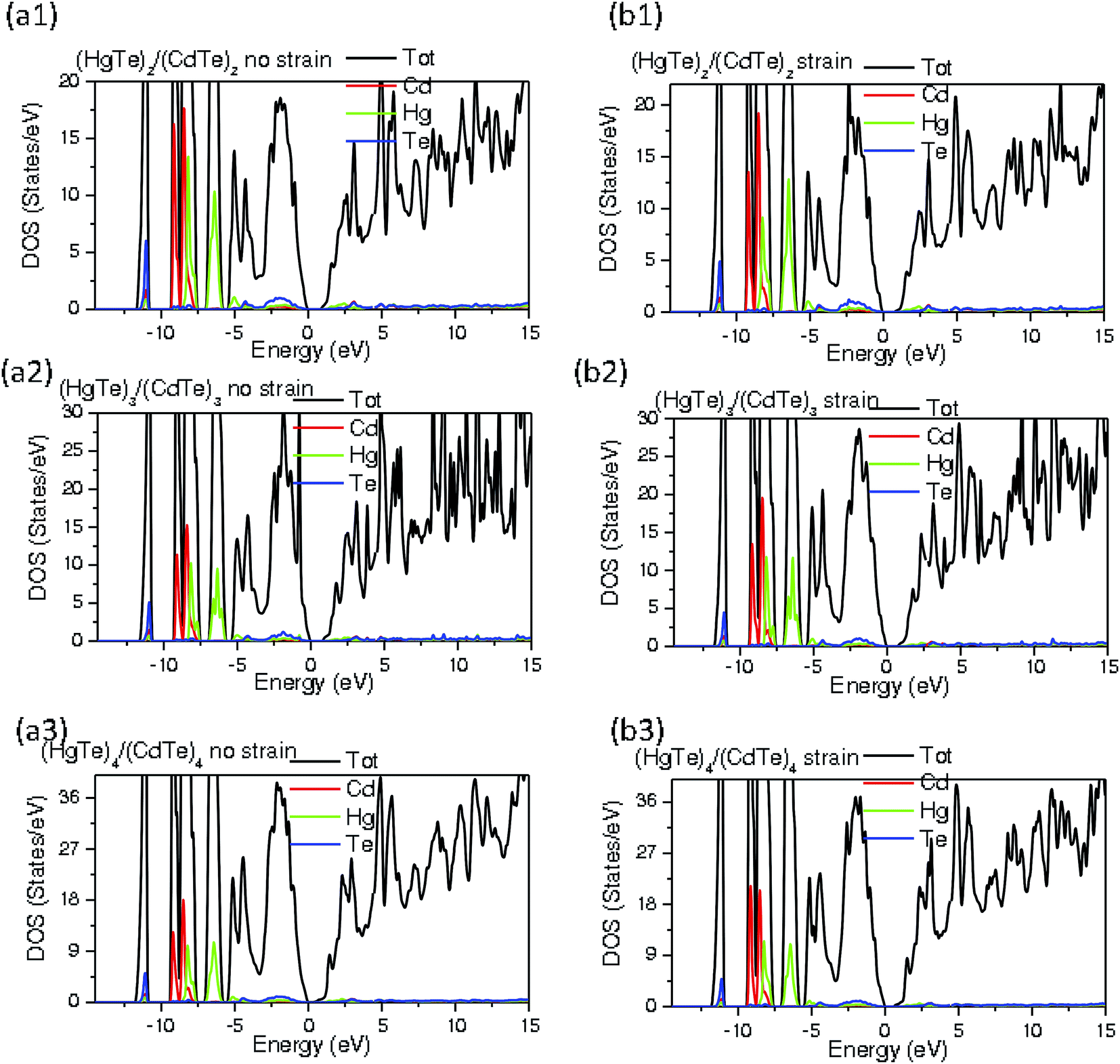 | ||
| Fig. 3 The total density of states and projected atomic density of states of (a1–a3) unstrained and (b1–b3) strained layers of (HgTe/CdTe)n superlattices (n = 2–4) grown along the (001) direction. | ||
The DOS profile of the (HgTe)4/(CdTe)4 SL exhibits the splitting of spectral peaks in the second region of the VB. By increasing the thickness, the LH in the strained HgTe/CdTe becomes almost pz-like, while the SO state becomes more px,y-like in character. Seemingly, the LH and SO states affect the p orbitals under the impact of strain. Meanwhile, when the value of periodicity is four in the (HgTe)n/(CdTe)n SLs, the DOS is mainly doubled with respect to the DOS profile of (HgTe)2/(CdTe)2 in both unstrained and strained (HgTe/CdTe) SLs. Indeed, this can be elucidated by the prominent contribution of Hg, Cd, and Te orbitals, in terms of the increased number of atoms when the number of layers is increased. As a matter of fact, the VBM of both HgTe and CdTe systems possesses the same anionic character. Apparently, the SOC effect influences the VBM containing the three detectable peaks, which are the split-off, LH, and HH bands. The fourth peak represents the CBs. Hence, the energy levels of HH and conduction states for these SLs are dominated by the order of the p-orbital energy. Also, the biaxial strain effect on the (HgTe)n/(CdTe)n SLs alters the orbital character of the electronic states and, therefore, it affects the optical properties. The DOS that includes the CBM illustrates the participation of the s/p-states of the Hg and Cd atoms. It seems that the strain has a small effect on the spectral properties of the VB edge states, as it slight changes the orbital character. Several previous studies have hitherto attempted to determine the VBM of the HgTe/CdTe (001) heterojunction by photoemission experiments.24,29,45,49–61
Optical properties of unstrained and strained (HgTe)n/(CdTe)n superlattices
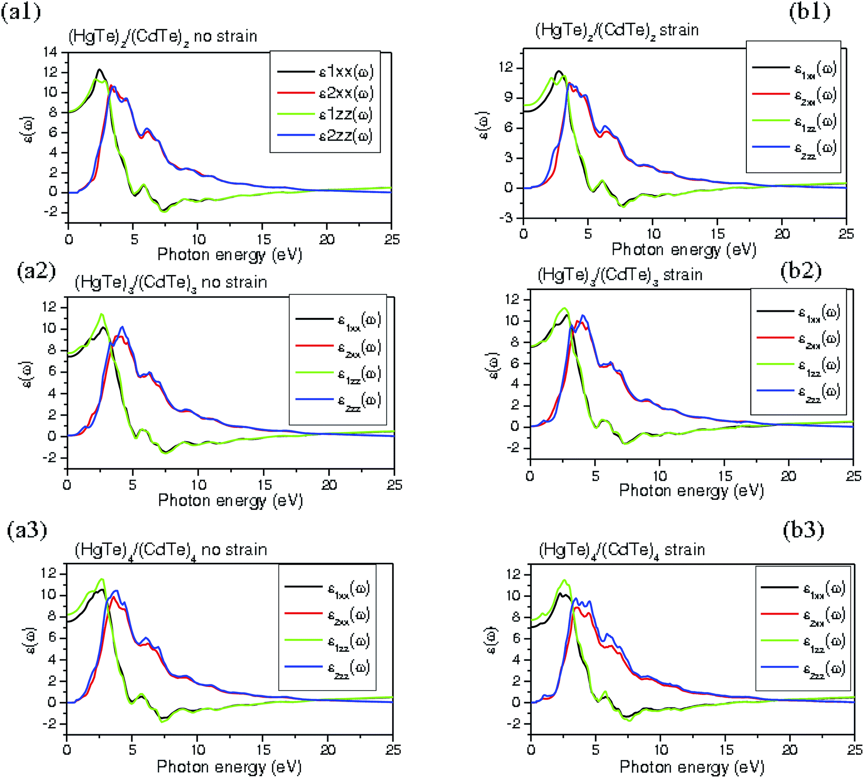
The knowledge of the optical characteristics of HgTe/CdTe SLs is crucial in understanding the physical nature of the band gap. The optical features of interest include band to band optical transitions, dispersion of the refractive index, and photon absorption. We present the effect of the strained layer along the (001) direction and thickness variation on the optical characteristics of the (HgTe)n/(CdTe)n SLs. Then, the dielectric function, ε(ω) as functions of the photon is computed for these SLs. In its complex form, the dielectric function is described as: ε(ω) = ε1(ω) + iε2(ω). The imaginary part ε2(ω) can be deduced directly from the band structure calculations, and the real part ε1(ω) can be deduced from the imaginary part ε2(ω). From ε1(ω) and ε2(ω), we can evaluate all other optical constants, such as the reflectivity R(ω), absorption coefficient α(ω), refractive index n(ω), energy loss spectra function L(ω), and optical conductivity α(ω).The calculated imaginary part ε2(ω) of the dielectric function is depicted in Fig. 4(a1–a3) and (b1–b3) for both unstrained and strained layers of (HgTe)n/(CdTe)n (n = 2–4) SLs grown on the (001) CdTe substrate. At first glance, all the SLs exhibit quite analogous ε2(ω) shapes over a broad span of energy, except for some minor spectral deviations. The main difference is that the spectrum shifts to the lower energy region when the thickness of the SL increases and the strain has a small influence on the considered SL. In general, the ε2(ω) plots of these SLs are quite similar over a broad span of energy values. For unstrained and strained (HgTe)2/(CdTe)2 SLs, the ε2(ω) is dominated by HgTe peaks at about 3.25 and 3.6 eV, whereas the CdTe content has a major participation in the proximity of the peaks at about 6.35 and 6.25 eV. A mixture of HgTe and CdTe is responsible for the intermediate energy peak (4.9 eV) in both unstrained and strained SL2. In the case of the (HgTe)3/(CdTe)3 SL, the first two peaks in the ε2xx (in-plane) and ε2zz (out-off plane) spectra are mainly dominated by the Hg content at 3.5 and 3.8 eV (unstrained SL), and at 3.3 and 4.8 eV (strained SL). As apparent, the ε2xx and ε2zz spectra exhibit that Cd–Te elements are responsible for the peaks at 6.43 and 6.5 eV, and at 6.3 and 6.4 eV in the unstrained and strained SLs, respectively. Sharp first peaks at 3.80 and 4.2 eV are observed in the ε2xx and ε2zz spectra of unstrained (HgTe)4/(CdTe)4 SLs, whereas the first set of peaks were situated at 3.7 and 3.9 eV in the spectra of the strained SLs. The second set of peaks are noticed at 6.40 and 6.3 eV, and 5.9 and 6.1 eV for the unstrained and strained SLs, respectively.
 | ||
| Fig. 4 Dielectric function of (a1–a3) unstrained (HgTe)n/(CdTe)n (n = 2–4) superlattices and (b1–b3) strained (HgTe)n/(CdTe)n (n = 2–4) superlattices. | ||
In all the SLs, it is seemingly that the structures of ε2(ω) are spectrally shifted towards lower energies with an increased amplitude when the number of the HgTe–CdTe layers varies. This is due to the fact that the decrement in the energy band gap versus the augmentation of the layers periodicity. On the other hand, the first perceptible peak of ε2(ω) is essentially due to the interband transition of the 5s–4d hybrid orbital of Cd and the 6s–5d hybrid orbital of Te to the 4p orbital of Te. The second peak is principally triggered by the interband transition of the 5p orbital of Hg and the 4p orbital of Te to the 6s orbital of Hg. The occurrence of third peak is attributed to the interband transitions of the 4p orbitals of Te/Cd atoms and the 5p orbital of Hg to the 6s orbital of Hg and the 5s orbital of Te at the critical point Γ. The quantum confinement effect is responsible for the various electronic transitions in the (HgTe)n/(CdTe)n SLs. In the strained layers of the (HgTe)n/(CdTe)n SLs, together with the confinement effects, the strain slightly affects the energy values, unlike in the case of the unstrained SLs. The absorption possesses a blue-shift that corroborates the increment of the band gap with the variation of the layer numbers in these SLs. The static optical dielectric constant ε0 plays an important role in microelectronic devices and is derived from the value of ε2(ω) at zero energy; it decreases with an increase in the layer thickness.40,62
The calculated real part, ε1(ω) of the dielectric function spectra are illustrated in Fig. 4(a1–a3) and (b1–b3) for unstrained (HgTe)n/(CdTe)n SLs (n = 2–4) and strained SLs along the (001) z-axis. For the (HgTe)2/(CdTe)2 SL (as seen in Fig. 4(a1) and (b1)), the ε1zz(ω) (in the z-direction) and ε1xx(ω) (in the basal-plane) illustrate strong peaks at approximately 2.35 and 2.5 eV in both unstrained and strained SLs. For the (HgTe)3/(CdTe)3 SL (Fig. 4(a2) and (b2)), the ε1zz(ω) and ε1xx(ω) exhibit sharp peaks at 2.6 and 2.5 eV in both unstrained and strained SLs. In Fig. 4(a3) and (b3), the ε1zz(ω) and ε1xx(ω) show marked peaks at around 3.7 and 3.80 eV in the unstrained and strained SLs, respectively. It is clearly surmised that all the SLs are isotropic in the basal-plane and z-directions in the regime beyond 5 eV. In the span between 0 and 5 eV, an anisotropy is noticed in the xy-plane and along the z direction. The difference between the two directions is small, leading to lesser anisotropy. It is obvious from the obtained results that increasing Hg content in HgTe/CdTe SLs renders the peaks sharper and shifts them towards lower photon energies. It is obvious that the high frequency dielectric constant ε1 (0 ≤ ℏEg) could be extracted in the basal-plane and along the z-axis. The calculated high frequency dielectric constants, ε∞, in the xy-plane and along the z-axis are listed in Table 1. For (HgTe)n/(CdTe)n SLs, the components of ε∞ = (ε∞x + ε∞y + ε∞z)/3 are ε∞⊥ = (ε∞x + ε∞y)/2, ε∞∥ = ε2, and Δε = (ε∥ − ε⊥), where ε∥ and ε⊥ are ε(ω) along the z and x directions, respectively. Δε is a constant that estimates the degree of anisotropy and it is to be kept in mind that the anisotropy in the high frequency dielectric constant is slightly increased in the strained SLs. The optical (high frequency) dielectric constant ε∞(0) is about 12.6 for the Hg0.8Cd0.2Te alloy40,44,62–64 and these values are in reasonable agreement with our bulk data. These earlier results seem to be compatible with the optical properties of the short period SLs and can be expected to provide information to understand these systems for better IR device design.36,55
![[thin space (1/6-em)]](https://www.rsc.org/images/entities/char_2009.gif)
Sophisticated theoretical techniques have been developed to provide an accurate description of the optical features of SLs at frequencies near the fundamental gap, including absorption coefficient. The absorption spectra can be described by the process of photon absorption which is due to the excitation of a VB electron to the CB. For the unstrained and strained (HgTe)n/(CdTe)n SLs, the absorption coefficients are depicted in Fig. 5(a1–a3) and (b1–b3). The computed absorption spectra of these SLs exhibit a behavior which is quite different from that of the binary bulk CdTe and HgTe,26 although it's reasonably close to their average. It is indicated that the threshold frequency decreases with the increase of layer thickness and strained layer along the (001) direction in the (HgTe)n/(CdTe)n SLs. This situation is not surprising since the energy gap is diminished with the augmentation of thickness and the effect of strain on the HgTe/CdTe SLs. The threshold energy in the absorption spectra is shifted to shorter wavelengths (higher energies) when the periodicity order is reduced. It is obvious that there is a change in the optical absorption coefficient of the unstrained and strained SLs when the layer periodicity is increased. Thus, a substantial peak appears only at energies greater than the optical energy gap and the optical absorption could be significant. The shape of the absorption coefficient curves of the (HgTe)2/(CdTe)2, (HgTe)3/(CdTe)3, and (HgTe)4/(CdTe)4 SLs show a slight similarity expect for the difference in the absorption edge. This is due to the change of layer thickness and SOC effect of Hg atom in the VBs that contribute to CdTe in each SL layer.
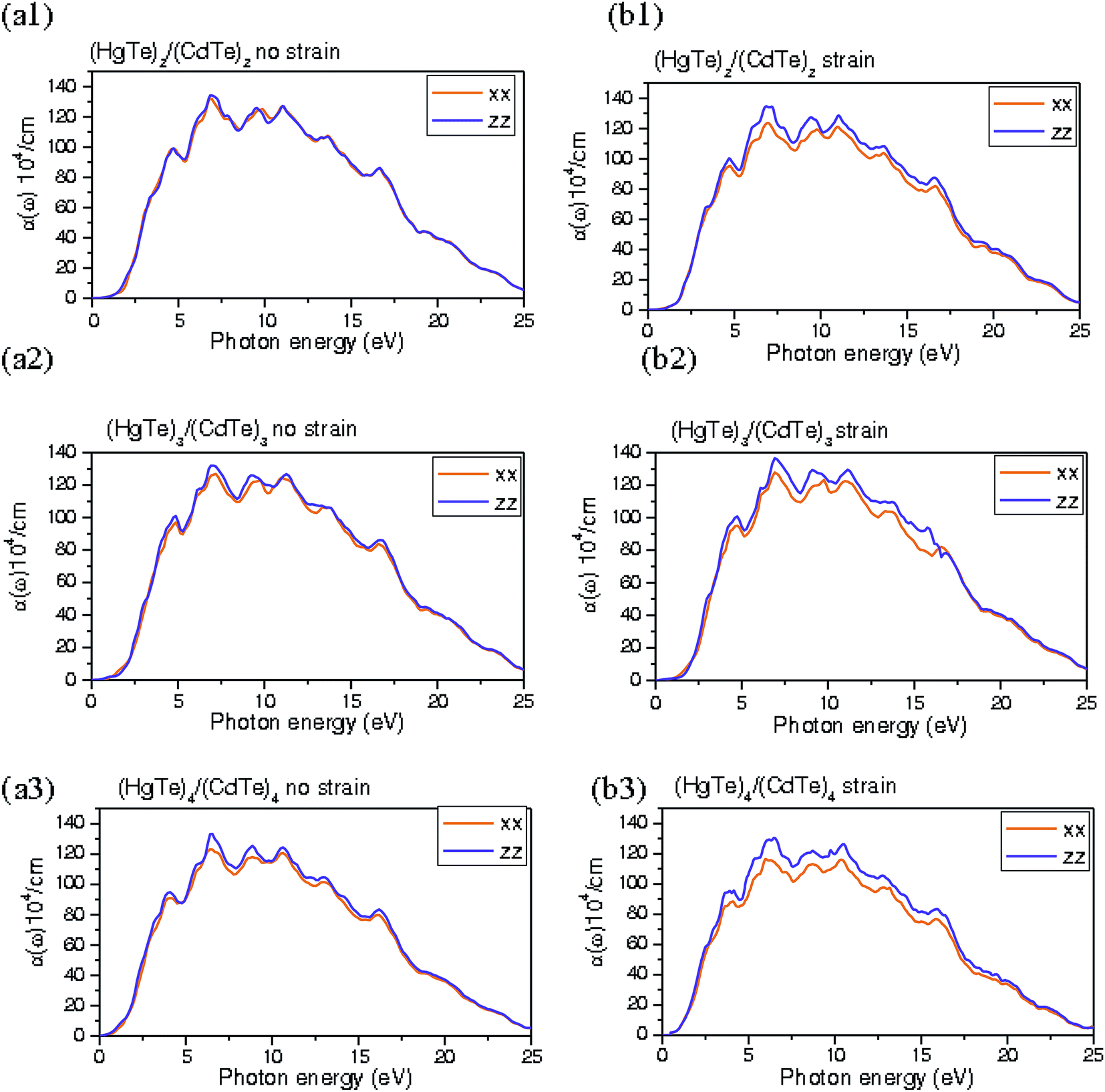 | ||
| Fig. 5 Optical absorption of (a1–a3) unstrained and (b1–b3) strained layers of (HgTe)n/(CdTe)n superlattices (n = 2–4). | ||
The absorption coefficient curves of the strained (HgTe)2/(CdTe)2, (HgTe)3/(CdTe)3, and (HgTe)4/(CdTe)4 SLs are quite similar to those of unstrained SLs. However, the insignificant difference in the absorption edge is a result of the strain-induced splitting of the light- and heavy-hole energies, in addition to the splitting caused by the quantum confinement effect in each SL layer. In the unstrained and strained (HgTe)2/(CdTe)2, (HgTe)3/(CdTe)3, and (HgTe)4/(CdTe)4 SLs, the absorption edge starts from 0.4 to 0.6 eV. It is clear that the substantial peak corresponding to the maximum absorption coefficient shifts to lower energies as a function of the layer thickness and strain effect on the SLs. A sharp peak emerges in the range of 5–8 eV in the absorption spectra of the unstrained and strained (HgTe)2/(CdTe)2, (HgTe)3/(CdTe)3, and (HgTe)4/(CdTe)4 SLs. The absorption coefficient features of the strained SLs illustrate a quite bigger anisotropy than the unstrained SLs. The optical absorption spectra along the z-axis are quite larger than those in the in-plane for all unstrained and strained (HgTe)n/(CdTe)n SLs along the (001) direction. The optical transition is quite significant since the CB and VB have different components, in spite of the band folding. The optical transitions are owing to the interface. This can be attributed to the optical transitions at the interfaces of HgTe and CdTe layers. It has been demonstrated that the absorption is a direct process, as anticipated, while the absorption edge was adjustable near 10 μm.56 These results confirmed that the HgTe/CdTe SLs possess the requisite optical properties for in IR optoelectronic devices and mid-IR detector applications. A measured near band edge absorption spectrum was generated for HgTe/(Hg0.15Cd0.85Te) SLs and compared with the previous calculated spectra in ref. 43 and 61–64. The experimental and calculated absorption spectra are quite identical to each other and followed a similar trend with layer thickness, as discussed in our work.
The reflectivity is a useful parameter to illustrate the optical nature in the short periodicity of HgTe/CdTe SLs along the (001) direction. A valuable parameter, the reflectivity coefficient, characterizes the reflective energy at the interface of the solid and can be deduced by the refractive index. Fig. 6(a1–a3) and (b1–b3) depict the reflection spectra Rxx(ω) and Rzz(ω) corresponding to the in-plane and z-direction, respectively, of the unstrained and strained HgTe/CdTe SLs grown the CdTe (001) substrates. The reflection spectra are recorded in the photon energy range of 0 to 25 eV. Obviously, it can be observed that the reflectivity increases at a low photon energy and decreases at a higher photon energy. It must be noted that the number of spectral peaks in the reflection spectra of HgTe/CdTe SLs is a function of the periodicity of layers. The main reason behind this phenomenon is that the electron and hole overlap increases by the confinement. The reflectivity characteristics of the HgTe and CdTe layers, depend on the layer thickness and periodicity.
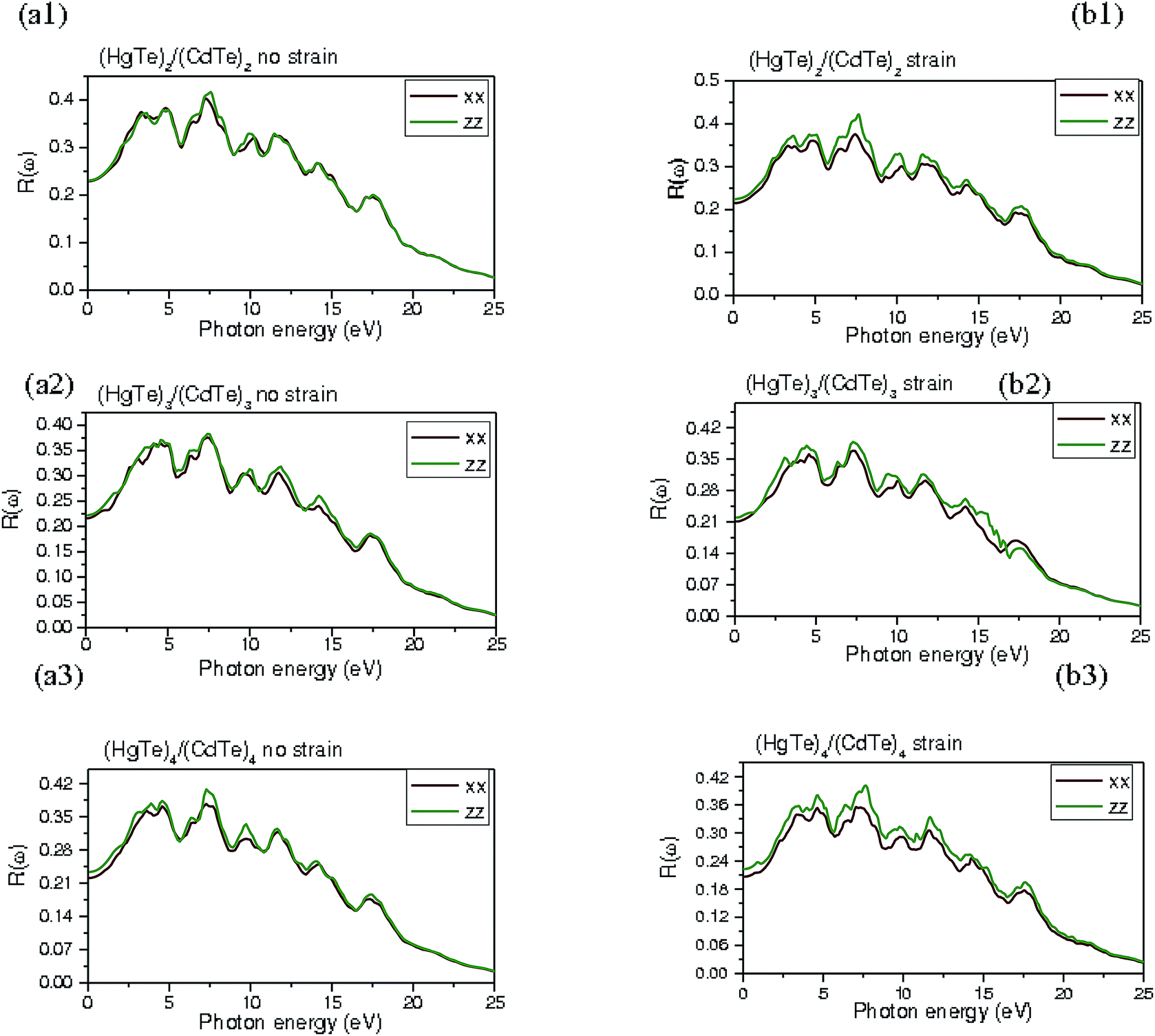 | ||
| Fig. 6 Reflectivity of (a1–a3) unstrained and (b1–b3) strained (HgTe)n/(CdTe)n (n = 2–4) superlattices. | ||
For unstrained SLs, the first set of peaks are remarkable at 3, 4.5, and 4.7 eV and the second set of peaks at roughly around 7.5 eV for (HgTe)2/(CdTe)2, (HgTe)3/(CdTe)3, and (HgTe)4/(CdTe)4 SLs, respectively. As seen, the reflectivity spectra of these SLs start from the zero frequency which defines the static part of the reflectivity, Rxx(0) and Rzz(0). The Rxx(0) values are equal to 0.24, 0.23, and 0.22 for (HgTe)2/(CdTe)2, (HgTe)3/(CdTe)3, and (HgTe)4/(CdTe)4 SLs, respectively. In addition, Rzz(0) values are about 0.237, 0.226, and 0.215 for these SLs at n values of 2–4, respectively. Note that the increase of thickness of the HgTe/CdTe SLs induces a slight low reflectivity. At energies less than 16 eV, an anisotropic behavior is present in the x- and z-directions (Rzz < Rxx). However, an isotropic behavior occurs in the energy regime higher than 16 eV (Rxx = Rzz). It is clear that the dispersion in the reflectivity spectrum of SL appears at low frequencies. This means that the increase of dispersion is due to a strong SOC in the shape of the HgTe layers.
For the strained layers in these SLs, the first set of peaks occurs at 3.8, 3.5, and 3.1 eV and the second observable peak is at 7.5 eV for the (HgTe)2/(CdTe)2, (HgTe)3/(CdTe)3, and (HgTe)4/(CdTe)4 SLs, respectively. The static parts of the reflectivity, Rxx(0), of the strained SLs are equal to 0.224, 0.216, and 0.210 for these SLs with n values variation from 2 to 4. Moreover, Rzz(0) values are approximately 0.228, 0.220, and 0.215 for the (HgTe)2/(CdTe)2, (HgTe)3/(CdTe)3, and (HgTe)4/(CdTe)4 SLs, respectively. At energies lower than 18 eV, an anisotropic nature is developed in the x- and z-directions (Rzz > Rxx), whereas an isotropic behavior is found in the section with greater energies (Rxx = Rzz) in the all SLs. Note that the main peaks are shifted to lower energies with an increase in the periodicity of SL layers. Previous transmission and reflection measurements for (001) Hg1−xCdxTe–HgTe SLs indicated energy gaps of around 0.68 ± 0.02 eV,15,16,31 which are in the same range as our theoretical findings. The first band corresponds to the HgTe-like sub-band and the second one to the CdTe-like sub-band. Mercury telluride is a semi-metal and therefore a decrease in the number of layers will lower the band gap, and this is expected to cause an increase in the plasma frequency.36,61–64
The refractive index of a semiconductor is a measure of its transparency to incident spectral radiation. However, the properties of these SLs are easily tailored since they exhibit a strong dependence on the thicknesses and strain of the constituent layers. The convenient calculations of the full polarization-dependent refractive index spectrum at photon energies near the fundamental gap would clearly be useful for designing such structures. In fact, the absorption properties at photon energies far from the gap play a dominant role in determining the magnitude of the near-gap refractive index of a system, however the detailed frequency dependence on the near-gap index emerges primarily from the absorption spectrum near the absorption edge. The refractive index as a function of the photon energy is displayed in Fig. 7(a1–a3) and (b1–b3) for (HgTe)n/(CdTe)n SLs (n = 2–4) with unstrained and strained layers along the (001) direction. Our results exhibit that the refractive index of the SL is dependent on the periodicity of the layers. It is clearly seen that the refractive index of the SL is augmented as the number of the HgTe and CdTe layers is decreased. This can be attributed to the high refractive index of HgTe as compared to CdTe. Thus, in these SLs, the refractive index values are lower than that of HgTe bulk, owing to the confinement effects.
 | ||
| Fig. 7 The refractive coefficient of (a1–a3) unstrained (HgTe)n/(CdTe)n superlattices and (b1–b3) of strained (HgTe)n/(CdTe)n (n = 2–4) superlattices. | ||
In the (HgTe)2/(CdTe)2 SL, the maximum intensity peaks are located nearby 2.58 eV (nxx = 3.62) and about 2.62 eV (nzz = 3.43). The intense sharp peak of (HgTe)3/(CdTe)3 SL is centered approximately at 2.48 eV (nxx = 3.25, nzz = 3.5), although for the (HgTe)4/(CdTe)4 SL, its location is approximately at 2.65 eV (nxx = 3.3, nzz = 3.62). The static refractive index value of  is around 2.81, 2.75, and 2.63 eV, while
  is in the vicinity of 2.85, 2.78, and 2.8 eV for (HgTe)2/(CdTe)2, (HgTe)3/(CdTe)3, and (HgTe)4/(CdTe)4 SLs, respectively. The significant sharp peak in (HgTe)2/(CdTe)2 is developed at around 2.75 eV (nxx = 3.62, nzz = 3.375), whereas its position in (HgTe)3/(CdTe)3 SL arises at nearly 3 eV (nxx = 3.25, nzz = 3.5). In the (HgTe)4/(CdTe)4SL, the peak position is at 3.15 eV (nxx = 3.25, nzz = 3.56). For strained layers, the static refractive index value of
  is roughly situated at 2.80, 2.69, and 2.60 eV, although
  is rather centered at 2.70, 2.75, and 2.76 eV for the (HgTe)2/(CdTe)2, (HgTe)3/(CdTe)3, and (HgTe)4/(CdTe)4 SLs, respectively. It is obvious that the pronounced spectral peaks of the xx and zz components of the strained SLs are shifted towards lower energies, when compared with the unstrained SLs. This indicates that a tensile strain in the HgTe/CdTe layers decreases the band gap. It is clear that the refractive index behavior, as a function of the photon energy, is isotropic in the span larger than 7.5 eV and anisotropic in the regime lesser than 7.5 eV for all periodic unstrained and strained SLs in the xy-plane and z direction. The refractive index of these SLs obtained at higher photon energies consists of an isotropic component which is related to the states far removed from the band edges and a smaller anisotropic component related to the Γ-transitions at frequencies near the band gap. Note that the birefringence can be used to predict the polarization which relies on the linear index of the transverse electric (TE) polarization and longitudinal electric (LE) polarization. For comparison, the refractive index of the unstrained SL is always larger than that of the strained SL, especially around the first transition between the quantized levels CB → HH-VB. The static refractive index value (n0) is found to decrease in strained SLs, unlike the unstrained SLs. This difference is attributed to the fact that these refractive indices originate from the strain caused by the small lattice mismatch. Then, it could be explained by the shift of the quantized levels by a few eV. The strained layers of HgTe/CdTe SLs alter somewhat the energy band structures near the sub-band edges. This could stem in modified inter-band optical matrix elements, and ultimately near-gap optical properties. Control of polarization anisotropies is highly desirable for the realization of polarization insensitive guided-wave structures based on HgTe/CdTe SLs. The experimental results compared favorably with other methods and validated these findings. It was exhibited that the refractive index is 3.4 and 3.29 corresponding to the energy band gap of 0.13 and 0.38 eV for Cd0.22Hg0.78Te and Cd0.28Hg0.72Te, respectively.61–63 This agrees reasonably with our theoretical evidence for both unstrained and strained SLs with short periodicity.
The energy loss function (ELF), L(ω), can describe the energy loss of a rapid electron traversing the material. The peak in the energy loss spectra represents the characteristics associated with the plasma resonance; the corresponding frequency is the so-called plasma frequency, ωp, which occurs when ε2 ≪ 1 and ε1 reaches zero. A small ε2(ω) at ε1(ω) = 0 leads to significant values of the ELF. It has the advantage of covering the complete energy span involving non-scattered and elastically scattered electrons (zero loss). The energy losses are primarily due to a complicated mixture of single electron excitations and collective excitations (plasmons). In the case of the inter-band transitions, which consist considerably of plasmon excitations, the scattering probability for volume losses is directly connected to the ELF. Fig. 8(a1–a3) and (b1–b3) represent the plots of the ELF spectra of the HgTe/CdTe SLs with varying layer thickness, involving both unstrained and strained layers along the (001) direction. All these spectra are plotted in the energy regime from 0 to 25 eV. It is to be noticed that these spectra include peaks and features, in addition to the plasmon peak, which are associated with the inter-band transitions. The plasmon peak is usually the remarkably intense feature in the spectrum at the point energy where the Re(ω) undergoes to zero, after the zero-loss peak.
 | ||
| Fig. 8 Energy loss function of (a1–a3) unstrained (HgTe)n/(CdTe)n and (b1–b3) strained layers (HgTe)n/(CdTe)n (n = 2–4) superlattices. | ||
For unstrained HgTe/CdTe SLs, the sharp spectral peaks are developed at around 17, 16.85, and 16 eV because of the occurrence of plasmon excitations in SL2, SL3, and SL4, respectively. Further, the peak positions of the strained layers SLs shift to lower energies in the vicinity of 16.5, 16, and 14 eV, respectively, for SL2, SL3, and SL4. Clearly, in the short periodicity of the unstrained (HgTe)n/(CdTe)n SLs, the main sharp peaks of the plasma frequency increase from 14.6 to 17 eV (CdTe) as the number of CdTe and HgTe layers increase for the xx and zz elements, respectively. Notably, the major peaks that are related to the zz element shift to higher energy levels when the SL layer thickness is varied, whereas these remarkable peaks shift towards lower energies in the case of the strained layers. This is mainly due to the energy loss function and the effective number of valence electrons that taking part in the inter-band transitions. For the strained SL layers, there is a strong peak at around 14–17.5 eV, which is related to the xx element in SL2 and SL3. The occurrence of the pronounced peak in SL4 is in the proximity of 14 eV and the number of spectral peaks increases, followed by peak splitting, because of the quantum confinement and SOC effect in this system. Several spectral peaks are present in the SLs when the number of layers increases (due to the quantum confinement effect), but a rather broad spectrum is noted for CdTe and HgTe compounds.26,30,43,48
Optical conductivity is believed to be a powerful probe in determining the electronic characteristics of a variety of materials. In general, if a system is subjected to an external electric field, a redistribution of charges occurs and current is induced. The optical conductivity spectra are generated in the energy range of 0–25 eV. The optical conductivity spectra σ(ω) of the unstrained and strained (HgTe)n/(CdTe)n SLs (n = 2–4) along the xy and z directions are illustrated in Fig. 9(a1–a3) and (b1–b3). The representative curves for the HgTe/CdTe SLs have several peaks corresponding to the bulk plasmon excitations which are caused by the electronic transitions from the VBs to the CBs. The variation of optical conductivity is illustrated as a function of the incident photon energy for all the SL systems. The increased optical conductivity at high photon energies is due to the high absorbance of CdTe and HgTe bulk in that regime. The optical conductivity and band gap indicate that the CdTe bulk can transmit within the visible span. In all the SLs, the conductivity is constant up to 1 eV, after which it increases with increasing photon energy. This indicates that the absorption of photon increases in the energy regime beyond 1 eV for unstrained and strained SLs. The conductivity peak of the unstrained and strained SLs is decreased, when compared to bulk CdTe and HgTe.31,36 The positions of the main peaks and the total widths of the optical conductivity bands for CdTe are 5 and 7.5 eV and about 5, 6.5, 7.5, and 11 eV for HgTe. However, some spectral features are not similar in unstrained and strained (HgTe)n/(CdTe)n SLs. This can be interpreted by the transitions between the quantized levels in these SLs. Two split sharp peaks are well seen in the 0–7.5 eV region for unstrained SLs. The first set of sharp peaks are located at 4.70, 4.45, and 4.35 eV, followed by the second set of peaks at 6.25, 6.16, and 6 eV for SL2, SL3, and SL4, respectively. A reduction in the optical conductivity is denoted by the minimum peaks in the 8.5–10 eV range for all the (HgTe)n/(CdTe)n SLs. Remarkably, the reduction in the conductivity of HgTe, is likewise due to a reduction in the depth of penetration of the electromagnetic waves in this regime. Apparently, SL2, and SL3 have isotropic behaviors unlike the SL4. It can be understood that as one undergoes from SL4 to SL2, the optical conductivity increases, which highlights the relevance of incorporating HgTe layers into CdTe.
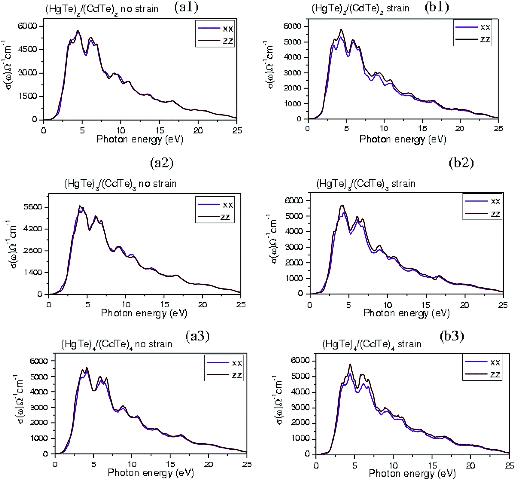 | ||
| Fig. 9 The optical conductivity for (a1–a3) unstrained (HgTe)n/(CdTe)n and (b1–b3) strained layers (HgTe)n/(CdTe)n SL's (n = 2–4). | ||
The increase in the optical conductivity indicates that the rate at which electrons absorb the incident photons at a given energy increases. One can also note that the optical conductivity has a strong dependence on the photon energy (wavelength) for HgTe and CdTe. However, the Hg 4s states participate in the upper part of the VB, while the Te 5s states prevail in the lower part of the CB. The s states of Te atoms and the s like states of Hg and Cd atom play a major role in these optical transitions as initial and final states for different thicknesses of the (HgTe)n/(CdTe)n SLs. It is seemingly that the strained SLs have sharp peaks which are quite different from those in unstrained SLs. It is well notable that many anisotropic featured peaks are procured in the energy regime less than 7.5 eV, along with a clear signature of isotropic behavior of the optical conductivity in the energy region of 7.7–25 eV. The optical conductivity spectra possess three appreciable peaks which are located at 2.9, 4.4, and 5.6 eV for strained SL2. As for the strained layers in SL3 and SL4, two discernible peaks arise at 4.6 and 5.6 eV. The anisotropic behavior in the optical conductivity increases at 5 eV upon varying the thickness of the (HgTe)n/(CdTe)n SLs. Furthermore, we detect that the optical conductivity spectra are also very sensitive to zz and xx polarization of the incident radiation in the strained SLs. Because the strained (HgTe)n/(CdTe)n SLs require to deposit two different materials together (HgTe-like and CdTe-like), the chemical bond symmetry breaks between the HgTe and CdTe layers and generates new anisotropy features according to the strained thickness. Overall, the electronic structure and the optical properties of these SLs are quite sensitive to the combination of the well and barrier layer thickness. This sensitivity suggests the possibility of designing suitable band structures which offer great potential for application in optical devices.
Conclusion
In this topical investigation, the electronic and optical characteristics of unstrained and strained layers of (HgTe)n/(CdTe)n SLs (n = 2–4) are simulated by employing the state-of-the-art FP-LAPW scheme. In this regard, the more trustworthy mBJ-GGA + SOC technique is compulsory for providing an improved depiction of the electronic, optical, and excited states. The electronic structure and optical characteristics of the undertaken SLs are compared when the theoretical and experimental results are accessible. We summarize our results in the following pivotal points:(1) By altering the layers number between 2 and 4, the resulting band structures of both unstrained and strained layers of (HgTe)n/(CdTe)n SLs have exhibited a direct band gap at the Γ point. The electronic states of HgTe/CdTe SLs are somehow affected by the strong SOC and band inversion which may lead to the splitting of the VBM of these SLs. A decrement in the energy gaps was found for the strained SLs in comparison with the unstrained SLs.
(2) Two essential factors dominate the swap in the energy gap of the (HgTe)n/(CdTe)n – the effect of the periodicity and the strained layers of the SLs. In fact, HgTe layers play a crucial role in controlling the energy gap of the SLs because of the quantum confinement impact in two dimensional systems. The proposionality of the layers number of the constituent elements is associated with the density of states of the SLs.
(3) From the inspection of the computed optical spectra (the dielectric function, absorption coefficient, reflectivity, refractive index, energy loss, and conductivity) of both unstrained and strained SLs, it was found that the spectral peaks shift towards lower energies with the variation of layers number and upon an introduction of strain in the HgTe and CdTe layers. In this respect, the optical spectra of the unstrained and strained SLs change their positions and peaks when the thickness is increased, this is accompanied by a narrowing of the band gap. Interestingly, the light absorption and emission of the HgTe/CdTe SLs are shifted to the IR span and are substantially enhanced when the layer thickness is reduced. Thus, HgTe/CdTe SLs could be promising for the fabrication of long-wavelength IR detectors.
(4) It is surmised that the ELF shifts towards lower energies when the SL thickness is increased. The corresponding spectral peaks in the strained SLs are weaker in intensity than in the unstrained SLs. The optical constants of the refractive indices of the HgTe/CdTe SLs exhibit anisotropy (birefringence) in two directions (in basal-plane and c-axis) because of the variation in the layer thickness and strain effects arising from the lattice mismatch in the HgTe/CdTe superlattice grown along the (001) direction of CdTe substrates. Hence, HgTe/CdTe SLs can be proposed as promising materials for the fabrication of long-wavelength infrared detectors. Credible and precise recognition about the effects of layer thickness and strain on the electronic structure and optical characteristics is of tremendous relevance to optimize group II–VI element based heterostructures for optoelectronic device applications.
Conflicts of interest
The authors declare no competing financial interests.Acknowledgements
This research project was supported by a grant from the “Research Center of the Female Scientific and Medical Colleges”, Deanship of Scientific Research, King Saud University.References
- E. R. Shaaban, N. Afify and A. El-Taher, Effect of film thickness on microstructure parameters and optical constants of CdTe thin films, J. Alloys Compd., 2009, 482, 400–404 CrossRef CAS.
- M. Burgelman, J. Verschraegen, S. Degrave and P. Nollet, Analysis of CdTe solar cells in relation to materials issues, Thin Solid Films, 2005, 480, 392–398 CrossRef.
- S. Shanmugan, S. Balaji and D. Mutharasu, Synthesis and characterization of 10% Sb doped CdTe thin films by stacked elemental layer (SEL) method, Mater. Lett., 2009, 63, 1189–1191 CrossRef CAS.
- S. K. Bera, D. Bhattacharyya, R. Ghosh and G. K. Paul, Spectroscopic ellipsometry of SiO2/CdTe nanocomposite thin films prepared by dc magnetron sputtering, Appl. Surf. Sci., 2009, 255, 6634–6640 CrossRef CAS.
- S. Subramani, D. Mutharasu and I. Kamarulazizi, Properties of Ag layered in Te/Cd stack prepared by stacked elemental layer method, Electron. Mater. Lett., 2012, 8, 263–268 CrossRef CAS.
- Y. Yang, H. Zhong, Z. Bai, B. Zou, Y. Li and G. D. Scholes, Transition from Photoconductivity to Photovoltaic Effect in P3HT/CuInSe2 Composites, J. Phys. Chem. C, 2012, 116, 7280–7286 CrossRef CAS.
- S. Chander and M. S. Dhaka, Physical properties of vacuum evaporated CdTe thin films with post-deposition thermal annealing, Phys. E, 2015, 73, 35–39 CrossRef CAS.
- B. Kumar, B. Rajesh, T. Hymavathi and S. Rao, Studies on optoelectronic properties of DC reactive magnetron sputtered CdTe thin films, AIP Conf. Proc., 2014, 1576(1), 73–75 CrossRef CAS.
- G. Zha, H. Zhou, J. Gao, T. Wang and W. Jie, The growth and the interfacial layer of CdZnTe nano-crystalline films by vacuum evaporation, Vacuum, 2011, 86, 242–245 CrossRef CAS.
- A. A. Al-Ghamdi, S. A. Khan, A. Nagat and M. A. El-Sadek, Synthesis and optical characterization of nanocrystalline CdTe thin films, Opt. Laser Technol., 2010, 42, 1181–1186 CrossRef CAS.
- M. N. Khan, N. Mahmood and A. A. Khurram, Structural and optical studies of laser ablated nanostructured CdTe thin films, J. Optoelectron. Adv. Mater., 2014, 16, 351–359 Search PubMed.
- R. S. Singh, et al., Nano-structured CdTe, CdS and TiO2 for thin film solar cell applications, Sol. Energy Mater. Sol. Cells, 2004, 82, 315–330 CrossRef CAS.
- B. Scharf, A. Matos-Abiague, I. Žutić and J. Fabian, Probing topological transitions in HgTe/CdTe quantum wells by magneto-optical measurements, Phys. Rev. B: Condens. Matter Mater. Phys., 2015, 91, 235433 CrossRef.
- V. Kaladzhyan, P. P. Aseev and S. N. Artemenko, Photogalvanic effect in the HgTe/CdTe topological insulator due to edge-bulk optical transitions, Phys. Rev. B: Condens. Matter Mater. Phys., 2015, 92, 155424 CrossRef.
- N. Romcevic, et al., Raman spectra of CdTe/ZnTe self-assembled quantum dots, Microelectron. J., 2009, 40, 830–831 CrossRef CAS.
- S. Kasap and A. Willoughby, Mercury Cadmium Telluride: Growth, Properties and Applications, ed. P. Capper, and J. Garland, John Wiley & Sons, 2011, vol. 38 Search PubMed.
- S. A. Khan, F. S. Al-Hazmi, S. Al-Heniti, A. S. Faidah and A. A. Al-Ghamdi, Effect of cadmium addition on the optical constants of thermally evaporated amorphous Se–S–Cd thin films, Curr. Appl. Phys., 2010, 10, 145–152 CrossRef.
- J. Li, G. Zou, X. Hu and X. Zhang, Electrochemistry of thiol-capped CdTe quantum dots and its sensing application, J. Electroanal. Chem., 2009, 625, 88–91 CrossRef CAS.
- N. Armani, et al., Role of thermal treatment on the luminescence properties of CdTe thin films for photovoltaic applications, Thin Solid Films, 2007, 515, 6184–6187 CrossRef CAS.
- Y. L. Wu, F. He, X. W. He, W. Y. Li and Y. K. Zhang, Spectroscopic studies on the interaction between CdTe nanoparticles and lysozyme, Spectrochim. Acta, Part A, 2008, 71, 1199–1203 CrossRef PubMed.
- J. H. Wang, et al., Modification of CdTe quantum dots as temperature-insensitive bioprobes, Talanta, 2008, 74, 724–729 CrossRef CAS PubMed.
- M. N. Secuk, et al., Ab-initio Calculations of Structural, Electronic, Optical, Dynamic and Thermodynamic Properties of HgTe and HgSe, Am. J. Condens. Matter. Phys., 2014, 4, 13–19 Search PubMed.
- J. E. Moore and E. Joel, The birth of topological insulators, Nature, 2010, 464, 194–198 CrossRef CAS PubMed.
- Y. Chang, et al., Performance and reproducibility enhancement of HgCdTe molecular beam epitaxy growth on CdZnTe substrates using interfacial HgTe/CdTe superlattice layers, Appl. Phys. Lett., 2005, 86, 131924 CrossRef.
- Y. Chang, et al., Performance and reproducibility enhancement of HgCdTe molecular beam epitaxy growth on CdZnTe substrates using interfacial HgTe/CdTe superlattice layers, Appl. Phys. Lett., 2005, 86, 131924 CrossRef.
- A. Laref, M. Alsagri, S. Laref, J. T. Yang, Y. C. Xiong and S. Ahmad Khandy, Relativistic effects on the electronic and optical characteristics of Cd1-xHgxTe alloys-based solar cell materials, J. Phys. Chem. Solids, 2019, 129, 368 CrossRef CAS.
- M. Ritze and R. Enderlein, Band structure and discontinuities of HgTe/CdTe superlattices: a theoretical study, J. Cryst. Growth, 1990, 101, 359–363 CrossRef CAS.
- S. P. Kowalczyk, J. T. Cheung, E. A. Kraut and R. W. Grant, CdTe-HgTe (
![[1 with combining macron]](https://www.rsc.org/images/entities/char_0031_0304.gif) ) Heterojunction Valence-Band Discontinuity: a Common-Anion-Rule Contradiction, Phys. Rev. Lett., 1986, 56, 1605 CrossRef CAS PubMed.
) Heterojunction Valence-Band Discontinuity: a Common-Anion-Rule Contradiction, Phys. Rev. Lett., 1986, 56, 1605 CrossRef CAS PubMed. - A. Qteish and R. J. Needs, Valence-band-offset transitivity at HgTe/CdTe, HgTe/InSb, and CdTe/InSb interfaces, Phys. Rev. B: Condens. Matter Mater. Phys., 1993, 47, 3714 CrossRef CAS.
- A. J. Ekpunobi, Reformulated tight binding calculation for band discontinuity at CdTe/HgxCd1−xTe heterointerfaces and their type I–type III transitions, Mater. Sci. Eng. B, 2005, 117, 1–4 CrossRef.
- W. N. Jeremy and W. W. John, Accurate electronic properties for (Hg,Cd)Te systems using hybrid density functional theory, Phys. Rev. B: Condens. Matter Mater. Phys., 2011, 84, 121308(R) CrossRef.
- W. Yang, K. Chang and S. C. Zhang, Intrinsic spin Hall Effect induced by quantum phase transition in HgCdTe quantum wells, Phys. Rev. Lett., 2008, 100, 056602 CrossRef PubMed.
- J. Li, et al., Two-dimensional topological insulators with tunable band gaps: single-layer HgTe and HgSe, Sci. Rep., 2015, 5, 14115 CrossRef CAS PubMed.
- Z. D. Kvon, E. B. Olshanetsky, D. A. Kozlov, N. N. Mikhailov and S. A. Dvoretskii, Two-dimensional electron-hole system in a HgTe-based quantum well, JETP Lett., 2008, 87, 502–505 CrossRef CAS.
- Z. D. Kvon, et al., Two-dimensional electron-hole system in HgTe-based quantum wells with surface orientation (112), Phys. Rev. B: Condens. Matter Mater. Phys., 2011, 83, 193304 CrossRef.
- N. N. Mikhailov, et al., Growth of Hg1−xCdxTe nanostructures by molecular beam epitaxy with ellipsometric control, Int. J. Nanotechnol., 2006, 3, 120–130 CrossRef CAS.
- E. B. Olshanetsky, Two-dimensional semimetal in HgTe-based quantum wells with surface orientation (100), Solid State Commun., 2012, 152, 265–267 CrossRef CAS.
- J. R. Lindle, et al., Efficient 3–5-μm negative luminescence from HgCdTe/Si photodiodes, Appl. Phys. Lett., 2003, 82, 2002–2004 CrossRef CAS.
- Y. U. Peter and M. Cardona, Fundamentals of semiconductors: physics and materials properties, Springer Science & Business Media, 2010 Search PubMed.
- I. C. Robin, M. Taupin, R. Derone, P. Ballet and A. Lusson, Photoluminescence studies of HgCdTe epilayers, J. Electron. Mater., 2010, 39, 868–872 CrossRef CAS.
- B. Bernevig, et al., Quantum spin Hall effect and topological phase transition in HgTe quantum wells, Science, 2006, 314, 1757–1761 CrossRef CAS PubMed.
- J. W. Luo and A. Zunger, Design principles and coupling mechanisms in the 2D quantum well topological insulator HgTe/CdTe, Phys. Rev. Lett., 2010, 105, 176805 CrossRef PubMed.
- S. W. Kim and K. S. Sohn, Optical properties of a multiple quantum well in a HgTe/CdTe system, J. Phys.: Condens. Matter, 1996, 8, 7619 CrossRef CAS.
- C. Brüne, et al., Quantum Hall effect from the topological surface states of strained bulk HgTe, Phys. Rev. Lett., 2011, 106, 126803 CrossRef PubMed.
- Z. D. Kvon, E. B. Olshanetsky, N. N. Mikhailov and D. A. Kozlov, Two-dimensional electron systems in HgTe quantum wells, Low Temp. Phys., 2009, 35, 6–14 CrossRef CAS.
- H. Zhiming and J. Chu, The refractive index dispersion of Hg1−xCdxTe by infrared spectroscopic ellipsometry, Infrared Phys. Technol., 2001, 42, 77–80 CrossRef.
- Z. Yang, et al., Optical properties of HgTe/CdTe superlattices in the normal, semimetallic, and inverted-band regimes, Phys. Rev. B: Condens. Matter Mater. Phys., 1994, 49, 8096 CrossRef CAS.
- X. Chu, S. Sivananthan and J. P. Faurie, Type III-Type I transition and strain-effect in Hg1−xCdxTe/CdTe and Hg1−xZnxTe/CdTe superlattices, Superlattices Microstruct., 1988, 4, 173–180 CrossRef CAS.
- J. Polit, Model of the two well potential for Hg-atoms in the Hg1−xCdxTe alloy lattice, Bull. Pol. Acad. Sci.: Tech. Sci., 2011, 59, 331–341 CAS.
- W. Kohn and L. J. Sham, Self-consistent equations including exchange and correlation effects, Phys. Rev., 1965, 140, A1133 CrossRef.
- P. Blaha, K. Schwarz, G. K. H. Madsen, D. Kvasnicka and J. LuitzWIEN2K, An Augmented Plane Wave Plus Local Orbitals Program for Calculating Crystal Properties, 2001 Search PubMed.
- J. P. Perdew, K. Burke and M. Ernzerhof, Generalized Gradient Approximation Made Simple, Phys. Rev. Lett., 1996, 78, 1396 CrossRef.
- F. Tran and P. Blaha, Accurate band gaps of semiconductors and insulators with a semilocal exchange-correlation potential, Phys. Rev. Lett., 2009, 102, 226401 CrossRef PubMed.
- A. M. Itsuno, J. D. Phillips and S. Velicu, Design and modeling of HgCdTe nBn detectors, J. Electron. Mater., 2011, 40, 1624–1629 CrossRef CAS.
- A. Rogalski, Infrared detectors: an overview, Infrared Phys. Technol., 2002, 43, 187–210 CrossRef.
- A. Rogalski, HgCdTe infrared detector material: history, status and outlook, Rep. Prog. Phys., 2005, 68, 2267 CrossRef CAS.
- D. Bertho, A. Simon, D. Boiron, C. Jouanin and C. Priester, Calculation of band offsets in strained II–VI heterojunctions, J. Cryst. Growth, 1990, 101, 372–375 CrossRef.
- N. E. Christensen, I. Gorczyca, O. B. Christensen, U. Schmid and M. Cardona, Band structure and heterojunctions of II–VI materials, J. Cryst. Growth, 1990, 101, 318–331 CrossRef CAS.
- E. L. Ivchenko, A. Y. Kaminski and A. Rossler, Heavy-light hole mixing at zinc-blende (001) interfaces under normal incidence, Phys. Rev. B: Condens. Matter Mater. Phys., 1996, 54, 5852 CrossRef CAS.
- C. R. Becker, Y. S. Wu, A. Waag, M. M. Kraus and G. Landwehr, The orientation independence of the CdTe-HgTe valence band offset as determined by X-ray photoelectron spectroscopy, Semicond. Sci. Technol., 1991, 6C, C76 CrossRef.
- P. M. Amirtharaj, N. K. Dhar, J. Baars and H. Seelewind, Investigation of photons in HgCdTe using Raman Scattering and far-infrared reflectivity, Semicond. Sci. Technol., 1990, 5, S68 CrossRef CAS.
- S. M. Hosseini, Optical properties of cadmium telluride in zinc-blende and wurzite structure, Phys. B Condens. Matter, 2008, 403, 1907–1915 CrossRef CAS.
- A. Noda, H. Kurita and R. Hirano, Mercury Cadmium Telluride Growth, Properties and Applications, ed. P. Capper and J. Garland, 2011 Search PubMed.
- Z. Huang and J. Chu, The refractive index dispersion of Hg1−xCdxTe by infrared spectroscopic ellipsometry, Infrared Phys. Technol., 2001, 42, 77–80 CrossRef CAS.
| This journal is © The Royal Society of Chemistry 2019 |