DOI:
10.1039/C8RA09433K
(Paper)
RSC Adv., 2019,
9, 6681-6688
Analysis and optimization of alloyed Al-p+ region and rear contacts for highly efficient industrial n-type silicon solar cells
Received
16th November 2018
, Accepted 13th February 2019
First published on 26th February 2019
Abstract
This paper aims to develop high quality screen-printed Al emitters and improve the interface condition of rear contacts in industrial silicon solar cells. We propose to introduce an ultra-thin SiO2 buffer layer between the silicon bulk and metal contact during the fabrication process. A post-annealing strategy is adapted to further modify the Al doping profiles. The experimental results show that the effects of this oxide layer on migrating the nonuniformity of Al-p+ region and decreasing the defects at the metal–silicon interface are significant. The recombination velocity of contacts, which is extracted from the measured Srear by an analytical model, exhibits a decrease by 90.8% and the series resistance is reduced by 60.3% for the improved contacts compared to the conventional screen-printed contacts. Finally, this technique is applied to large-area (156 × 156 mm2) industrial n-type silicon solar cells and leads to a 2.18% increase in average cell efficiency, including a 12.82 mV increase in open-circuit voltage Voc and 0.99 mA cm−2 increase in short-circuit current density Jsc compared with solar cells fabricated by a standard industrial process. A 19.16% efficient cell with a Voc of 637.47 mV is achieved.
1 Introduction
Recently, n-type silicon solar cells have received increased attention for industrial applications, such as the n-type rear-junction Passivated Emitter Rear Totally-diffused (PERT) solar cells.1–3 However, laser ablation and high-temperature boron diffusion techniques (∼1000 °C) are necessary in the fabrication process of PERT solar cells, which inevitably increases the damage and heat induced defects, as well as the fabrication cost. To achieve a more simplified and cost-efficient process while still being able to reach high efficiency, a screen-printing method is increasingly used in industrial crystalline cells.4,5 The Al-p+ region, which is alloyed from Al pastes, provides an ohmic contact and is commonly used as an emitter in new concept n-type cells, such as the n+np+ front-contact cells6–10 and the interdigitated back contact (IBC) cells.11,12 Recent publications have indicated that the electrical properties of the Al-p+ region and contacts significantly influence the cell performance and are considerably affected by the fabricating conditions. In the industrial alloying process, the screen-printing Al-paste is fired in a belt furnace with peak temperatures at about 800 °C to 900 °C.13 Si starts to melt into Al at 660 °C and forms an Al–Si liquid state. It recrystallizes again during cooling, while some Al atoms remain in the Si crystal lattice and form the Al-p+ region.14–16 Generally, the re-solidification is complete within several seconds and is assumed to be under non-thermal–equilibrium conditions; such a quick formation process usually introduces agglomerations and voids at the interface of Si–Al in industrial solar cells. Furthermore, the alloying reaction starts locally at the contacting points between Al and Si, and forms local Si–Al liquid melt on the wafer surface, which causes thickness inhomogeneities in the Al-p+ region. These disadvantageous effects strongly influence the field effect of the p–n junction and the ohmic contact. It is known that applying a thicker paste and increasing the alloying temperature can mitigate the thickness inhomogeneity.17,18 Nevertheless, a thicker paste usually aggravates wafer bow due to the contrast of thermal expansion coefficients between Si material and Al paste matrix after firing. Moreover, Al–O defect centers are inevitably introduced due to high temperature treatment,19 which leads to the decrease of carrier lifetime in devices. Therefore, the uniformity control and the understanding of the recombination in Al-emitters are of prime importance for solar cell design strategies and process optimization.
The aim of this paper is to improve the electrical properties of Al-p+ layer and the interface condition of rear contacts in n-type silicon solar cells. We focus on their formation process and develop an industrially applicable method to integrate an ultra-thin SiO2 buffer layer at the Si–Al interface. To determine the contact recombination velocities of the Al-alloyed rear contacts, area-averaged carrier lifetimes measured by the microwave-detected photoconductance decay (MWPCD) technique are analyzed.20 In contrast to the typical industrial fabricating process, the beneficial effects of such a thin layer on mitigating the nonuniformity of the Al-p+ region and decreasing the defects at the metal–silicon interface are presented. Finally, large-area (156 × 156 mm2) industrial n-type Si solar cells featuring full-area and improved Al rear emitters are fabricated.
2 Experimental details
All the samples in this study were prepared on (100)-oriented Czochralski (Cz) n-type silicon wafers of 1–3 Ω·cm resistivity, with a thickness of 200 μm. After RCA cleaning followed by a HF dip, the test samples for SEM and ECV measurements were polished with a special solution. The Al-p+ region is formed by firing the screen-printed Al pastes in an industrial conveyor belt furnace. The samples for Quasi-Steady-State Photoconductance (QSSPC) lifetime measurements are silicon samples with pyramidally textured/polished front surface and passivated with SiNx. The lifetime of the starting wafers (bare n-type silicon, 52 × 52 mm) are about 1.9 μs. The rear surface is Al screen-printed, and is fired under industrial conditions. The residual Al paste and the Al–Si eutectic on ECV and QSSPC samples are finally removed in a boiling 37% solution of HCl. For the studies on solar cells, we fabricate cells in two groups for comparison. The group 1 cells are fabricated by a standard industrial process. In group 2, the cells are with an interfacial oxide layer. The fabrication flow chart is demonstrated in Fig. 1. The cells are all of front Ag contact back-junction structure, with SiNx front surface field (FSF) passivation, processed on 156 × 156 mm2 wafers. After industrial texturing and RCA cleaning, we perform an n+ FSF phosphorus diffusion on the textured front surface, resulting in a FSF sheet resistance of 59 Ω sq−1. The phosphorus silicate glass (PSG) is subsequently etched off in HF solution. To form a polished rear surface, we performed a single side wet chemical etch of about 3 μm. The oxide thin layers are grown from thermal oxidation at 860 °C on both sides of the samples, and then washed off from the front surface by HF solution. This SiO2 layer is estimated to be 1.86 nm by ellipsometry measurement. Afterwards, an 80 nm-thick SiNx layer with a refractive index n = 2.0 is deposited on the front side of the wafers by an in-line microwave Plasma Enhanced Chemical Vapor Deposition (PECVD) system. A conventional grid pattern on the front and a full area pattern on the rear are screen-printed by using Ag and Al pastes, respectively. The Al-p+ emitters and the contacts are formed in an infrared conveyor belt furnace by a co-firing process at 880 °C for 13 s. In order to characterize the surface recombination velocity of metallized rear surfaces, lifetime measurements were performed by MWPCD measurements. The wafers were cleaned and polished in a wet chemical process. We defined 23 contact geometry with an area of 25 × 25 mm on each 156 × 156 mm2 wafer. The geometries vary in contact pitch p (ranging from 300 to 3500 μm) and contact width a (ranging from 80 to 500 μm). We completed the contact formation by full-area screen printing Al paste at approximately 880 °C and finally an 80 nm-thick SiNx layer was deposited on both sides of the wafers by PECVD.
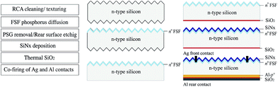 |
| | Fig. 1 Process flow of the solar cells in group 2. | |
3 Results and discussion
3.1 Influence on the formation of the homogeneous Al-p+ layer
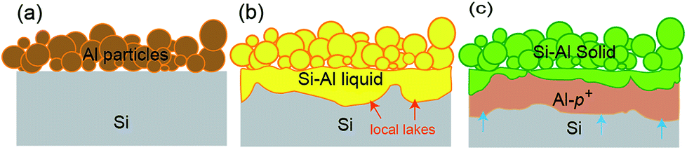
(i) Formation of Al-p+ region. The Al-emitter is generally formed in a belt furnace with peak temperatures around 800 °C to 900 °C in the contact firing step of solar cell fabrication. Fig. 2 shows the formation process of Al-p+ regions and the rear contact from a screen-printed aluminium paste. After the burn-out of the organic components in the pastes, the alloying process starts with the melting of the Al at 660 °C. The liquid aluminium locally penetrates the shells of the Al particles to make contact with the silicon surface to start the melt with Si, and to neighbouring Al particles. It is important to notice that the Al paste particles are held in place by the matrix during the whole firing process and the transport of the liquid Si–Al takes place from particle to particle via small sintering necks.14 The alloying reaction thus starts locally on the wafer surface, leading to the formation of liquid “lakes” on the wafer surface, as demonstrated in Fig. 2(b). According to the formation model of M. Rauer,17 when the Al–Si melt on the surface exceeds a critical thickness, it starts to contract to minimize the interface tension between Al–Si liquid and solid Si wafer, leading to melt accumulation and depletion. On cooling down, silicon is rejected from the melt and recrystallizes epitaxially on the wafer surface. As the accumulated regions effectively provide a higher amount of Al–Si melt, the Al-p+ region growth is enhanced within these regions. The residual Al–Si melt solidifies at the eutectic temperature of 577 °C, building a compact Al–Si layer of eutectic composition on top of the Al-p+ region, as shown in the sketch in Fig. 2(c). This model explains the formation of lateral thickness inhomogeneities in the Al-p+ region.
 |
| | Fig. 2 Sketch of the formation of Al-p+ regions and rear contact from a screen printed aluminium paste. (a) After drying (removal of solvents) a porous paste matrix of aluminium particles is attached to the Si wafer surface. (b) The alloying process starts with the melting of the aluminium at 660 °C. The liquid aluminium dissolves silicon, forming local Si–Al liquid “lakes” on the wafer surface. (c) On cooling down after reaching the eutectic temperature of 577 °C, an Si–Al solid layer is present on top of the Al-p+ region. Arrows indicate the enhanced thickness due to locally accumulated Si–Al liquid. | |
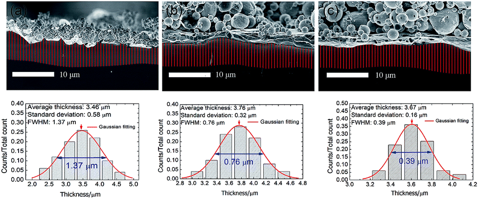
(ii) Thickness homogeneity. The thickness of the Al-p+ layer is determined by the amount of Si dissolved into the Al–Si melt at the peak temperature. Theoretical calculations reveal that increasing the thickness of the deposited Al pastes or peak alloying temperature can improve the quality of the Al-p+ region. However, high temperatures tend to degrade the Al emitter quality as a result of nonuniformity triggered by the agglomeration of Al–Si melt in combination with the bandgap narrowing due to the high doping effect. Moreover, it is found that the critical temperature above which the solar cell performance starts to degenerate is lower for thicker Al layers, which puts a limit on the maximum thickness that can be achieved.21Since the liquid Al transports through sintering necks between paste particles to make contact with Si, the locally started reaction between Si and Al can not make full coverage of the surface. Therefore, the morphology of the Si surface, as well as the presence of an interface layer becomes important to the homogeneity of the Al-p+ layer. In Fig. 3, scanning electron microscope (SEM) images of the cross section of the Al-doped p+ regions realized from different surface conditions are shown. Due to the potential contrast between the Al-p+ region and the Si base, the Al-p+ regions are clearly visible.
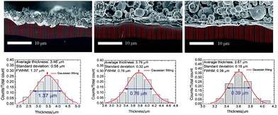 |
| | Fig. 3 SEM images of the cross-section of Al-doped p+ regions at Si surfaces. The samples are of (a) a pyramidally textured Si surface, (b) a polished Si surface, (c) a polished and oxidized Si surface. All the three samples are fired at the same industrial condition of 880 °C. Direct measurements of the Al-p+ region thickness are performed, as marked red for (a)–(c). A Gaussian distribution is fitted to each measured result, as shown below the images. | |
In order to compare the influence of the surface morphology and the SiO2 interface layer on homogeneity, the thickness distributions of the Al-p+ region cross-section are measured.22 Fig. 3(a) shows a discontinuous alloy layer at the Si–Al interface for the pyramidally textured sample. The tops of the pyramidal structures on the rear surface are completely melted, some bottom parts inadequately contact with the Al paste which results in an average thickness of 3.46 μm and full width at half maximum (FWHM) of 1.37 μm in the Gaussian fitted profile, as shown in the graph below the image. This situation can be improved using a polished surface as shown in Fig. 3(b), the alloy layer is more continuous whereas the interface is still rough with abrupt tips and occasional cracks. The average thickness is 3.76 μm and FWHM is 0.76 μm. In Fig. 3(c), we apply a thin SiO2 layer on the polished Si surface before screen-printing. It is clearly seen that the Si–Al alloy layer exhibits more smooth and uniform properties. The average thickness is 3.67 μm and FWHM is reduced to 0.39 μm, a remarkable effect on homogeneity is observed. It is believed that the SiO2 layer works as a buffer, which slows down the immediate contact between Al particles in the paste and Si surface during the firing process. This effect thus reduces the large amount of melt at the agglomerated regions, resulting in a more uniform Al-p+ layer over a wide range.
3.2 Influence of the post-annealing conditions
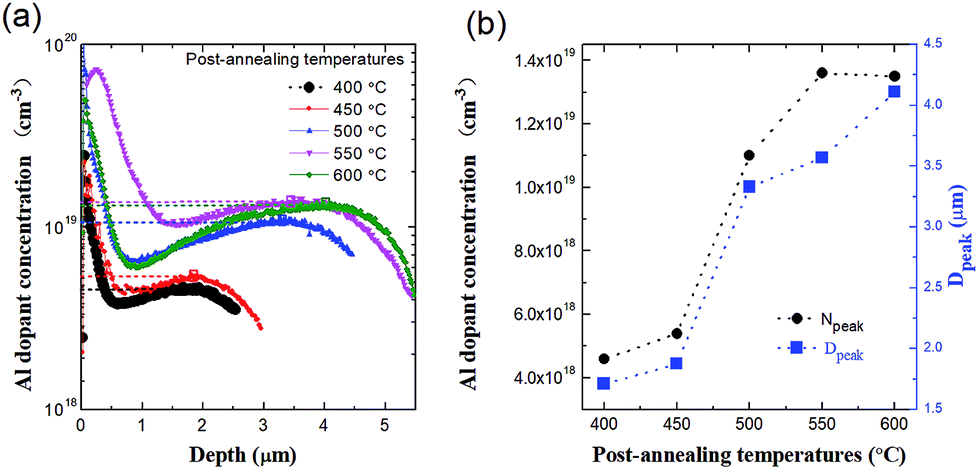
(i) Influence on Al diffusion profiles. Due to the fact that the Al-p+ regions placed on the rear side of a solar cell work as a p–n junction in n-type back-junction solar cells, the diffusion depth and doping level of Al are essential to form a reasonable electrical field to separate the charge carriers and enable diffusion of minority carriers. In order to modify the Al diffusion profile and improve the performance of solar cells, we adopt a post-annealing strategy after the firing process. Five Al doped silicon samples under different diffusion conditions are prepared to determine the influence of different doping levels, and the thickness of the Al-p+ region. The post-annealing treatments are kept at 400 °C, 450 °C, 500 °C, 550 °C and 600 °C in ambient air, the annealing time is 20 min. The peak concentration Npeak and its corresponding depth position dpeak are extracted from the Al doping profile curves of Fig. 4(a). As seen in Fig. 4(b), the annealing treatments provide higher doping levels and thicker Al-p+ layer depths. As the temperature rises to 550 °C and above, it seems that the Al doping concentration reaches a maximum value and maintains a constant level as the annealing temperature rises, while the junction depths increase further. Al bumps begin to be observed at screen-printed surfaces at 600 °C. It is suspected that the driving force for the agglomeration is to reduce the interface energy between the Al–Si melt and Si by minimizing the contact interface area. This occurs by the formation of a higher contact angle, which produces the bumps.21
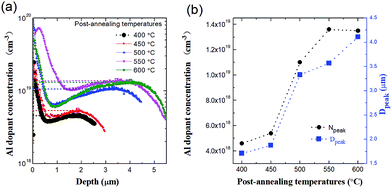 |
| | Fig. 4 (a) Al doping profiles of silicon samples under different post-annealing temperatures. (b) The peak doping concentration of Al as a function of post-annealing temperatures. All samples are screen-printed with industrial Al pastes and fired in an infrared conveyor belt furnace at 880 °C for 13 s. The post-annealing temperature is varied from 400 °C to 600 °C for 20 min. | |
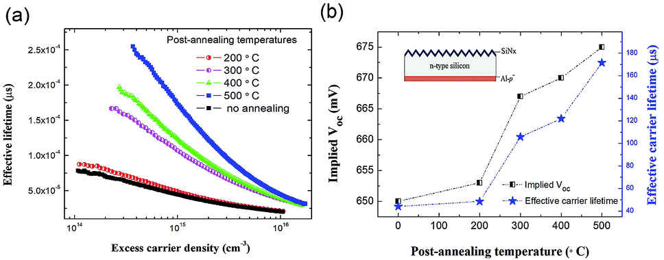
(ii) Influence on effective lifetime. In order to determine the influence of post-annealing on effective lifetime (τeff), injection-dependent lifetime measurements were performed by the QSSPC technique.23,24 The implied open-circuit voltage iVoc at one sun is used to determine the voltage of the device if contacts were applied, when only the recombination of the investigated emitter is considered. In Fig. 5(a) and (b), the τeff values and iVoc at 1 sun are plotted as a function of the post-annealing temperature. The improvement in lifetime is quite clear, the τeff curves for samples which suffer a post-annealing treatment are higher than those of the samples without annealing, as shown by the red, magenta, green and blue curves. The lifetime values can be gradually boosted as the annealing temperature increases from 200 °C to 500 °C. The corresponding lifetime values have been extracted from Fig. 5(a), as shown by the right axis in Fig. 5(b). A similar trend is also observed from the annealing condition dependent iVoc curves, which exhibit a high value of 675 mV at the annealing temperature of 500 °C.
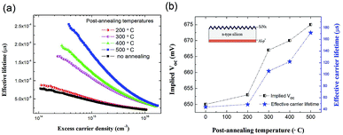 |
| | Fig. 5 (a) Measured injection dependent effective minority carrier lifetime for pyramidally textured samples with different post-annealing conditions. (b) Implied Voc and effective carrier lifetime as a function of the post-annealing temperature. The injection level is kept at 1015 cm−3. The structure of the test samples is sketched in the inserted graph. The drawn dot dash lines are guides to the eye. | |
To further investigate the influence of the annealing condition on τeff and find an optimal condition for solar cell treatment, a more meticulous work was performed with a set of samples which were annealed at various temperatures and times. The test samples are of n-type silicon with polished and passivated front surface, and Al-p+ back surface field. The QSSPC measurements were performed at an injection level of 1015 cm−3. As shown in the three-dimensional diagram of Fig. 6, the annealing conditions varied from 400 to 600 °C, for 10 to 60 min. It can be seen that the τeff of the samples increased with the annealing time at 400 °C. When annealed at 500 °C, the τeff reached the highest value at an annealing time of 30 min and then began to decline as the time increased to 45 and 60 min. For this same annealing time, the τeff of the sample annealed at 500 °C was greater than that of the sample annealed at 400 °C. However, when the annealing temperature reached 600 °C, the τeff of the samples clearly decreased. And with the increase of annealing time, the τeff tended to be lower. This is because the Al bumps are greatly enhanced at 600 °C, forming a large number of surface defects and locally high-doped regions, resulting in an increase of surface recombination and Auger recombination. Considering that prolonged annealing can cause agglomeration and damage to the sample, the longer the annealing time is, the more defects will be generated, we thus chose 500 °C for 30 min as the optimum annealing conditions.
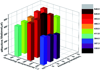 |
| | Fig. 6 Measured effective minority carrier lifetimes for samples annealed at different conditions. The temperatures are varied from 400 to 600 °C, for 10 to 60 min. The injection level is maintained at 1015 cm−3. | |
3.3 Recombination in Al-p+ region
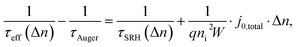
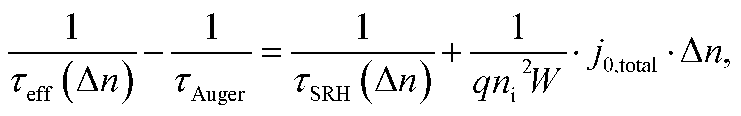
The saturation current densities of the Al-p+ regions (j0,Al) can be experimentally determined via the QSSPC measurements. Under high-level injection conditions, the recombination rate in the Al-p+ region has a quadratic dependence on the carrier density, as expressed in eqn (1)25,26| |
 | (1) |
where τSRH is the bulk Shockley–Read–Hall (SRH) lifetime, τAuger is the bulk Auger lifetime, j0,total is the total saturation current density, q is the elementary charge, ni is the intrinsic carrier density, Δn is the excess carrier concentration, and W is the wafer thickness. According to the slope method,27,28 the  curve shows a linear dependence of Δn, which can be used to extract j0,total. For our asymmetric samples, the saturation current density of the Al emitter (j0,Al) can be extracted by j0,Al = j0,total − j0,residual. The saturation current density of samples without Al-p+ region (j0,residual) can be determined with the help of an additional symmetric reference. The j0,Al for the sample with SiO2 and treated under 500 °C for 30 min is found to be 209.5 ± 44.5 fA cm−2, exhibiting a marked decrease of 1.54 pA cm−2 compared with the standard processed sample.
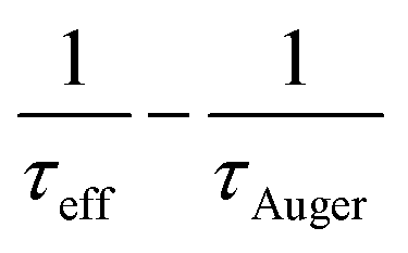
For n-type Si solar cells where the Al-p+ regions act as rear emitters, the thicknesses of the Al-p+ regions directly affect the screening of electrons from the metallized, recombination-active rear surfaces. Therefore, it influences the open-circuit voltage Voc and the maximum attainable efficiency of solar cells. Fig. 7 shows the simulated j0,Al as a function of Al doping depth. The model considers the influence of SRH recombination and Auger recombination, and takes the effect of incomplete ionization of Al acceptors into account.29–31 In Fig. 7(a), the minority carrier surface recombination velocity of the Al-p+ side Sr has been varied from Sr = 100 cm s−1 to Sr = 108 cm s−1, assuming the defect density Nt is 9 × 1014 cm−3.29,32 When the surface is perfectly passivated (Sr = 100 cm s−1), the saturation current density j0,Al is quite low under 300 fA cm−2. Due to the fact that the defect traps increase in the doped region, the rising trend of j0,Al with the increase of the Al emitter thickness can be seen. Similar trends can also be observed for 2.6 × 10³, 8 × 10³ and 104 cm s−1 curves. For Sr = 1.5 × 104 cm s−1, the j0,Al characteristics become nearly constant. With increasing Sr values, j0,Al rises quite quickly especially for relatively poorly passivated emitters (Sr > 1.5 × 104 cm s−1) at low Al profile depths. The j0,Al profiles decline with the Al-p+ region thickness, and this trend is more significant with the increase of Sr. The reason is that the field passivation effect by preventing the minority carriers to the surface is enhanced for thicker Al-p+ depths, leading to weakened recombination at the surface and a decrease in j0,Al.
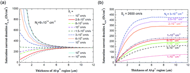 |
| | Fig. 7 Simulated results of saturation current densities of Al emitter as a function of doping depth. The sample structure is of SiNx passivated front surface and the rear surface is Al screen-printed, as shown in the inset of Fig. 5(b). The doping profile at 500 °C in Fig. 4(a) is used for simulations. The SRH recombination, the Auger recombination, and the effect of incomplete ionization of Al acceptors are considered in the simulation model. (a) The Sr is varied from 100 to108 cm s−1 and the Nt is 9 × 1014 cm−3. (b) The influence of the defect density, Nt is varied from 1 × 1014 cm−3 to 3 × 1015 cm−3 and Sr is 2600 cm s−1. | |
3.4 Determination of recombination velocity around Al contacts
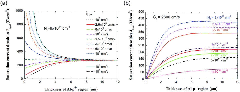
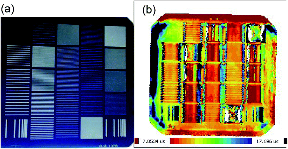
In order to characterize the surface recombination velocity Smet of metallized rear surfaces, we follow the approach presented in ref. 33 and 34, MWPCD measurements were performed to obtain the area-averaged effective rear surface recombination velocity Srear for each single 25 × 25 mm2 area in the test wafers. The image of the test sample and the MWPCD lifetime mapping is shown in Fig. 8. For high tBulk and low surface recombination velocities, the effective carrier lifetime is approximated by35| |
 | (2) |
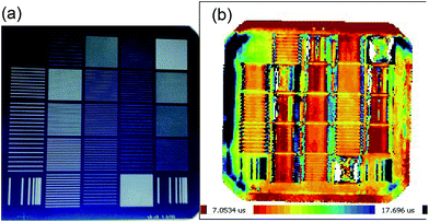 |
| | Fig. 8 (a) Image of test sample for the measurements of recombination at Al contacts. (b) Lifetime mapping of the test sample, measured by MWPCD. The sample consists of 23 areas of 25 × 25 mm on the 156 × 156 cm2 wafer. The pitch p varies from 300 to 3500 μm and contact width varies from 80 to 500 μm. | |
Fischer’s analytical model describes the area averaged effective rear surface recombination velocity,36 which is a function of the base series resistance Rs, the sample thickness W, the diffusion coefficient D, the metallization area fraction f, the surface recombination velocity in the passivated area Spass as well as the surface recombination velocity under the contact Scont.
| |
 | (3) |
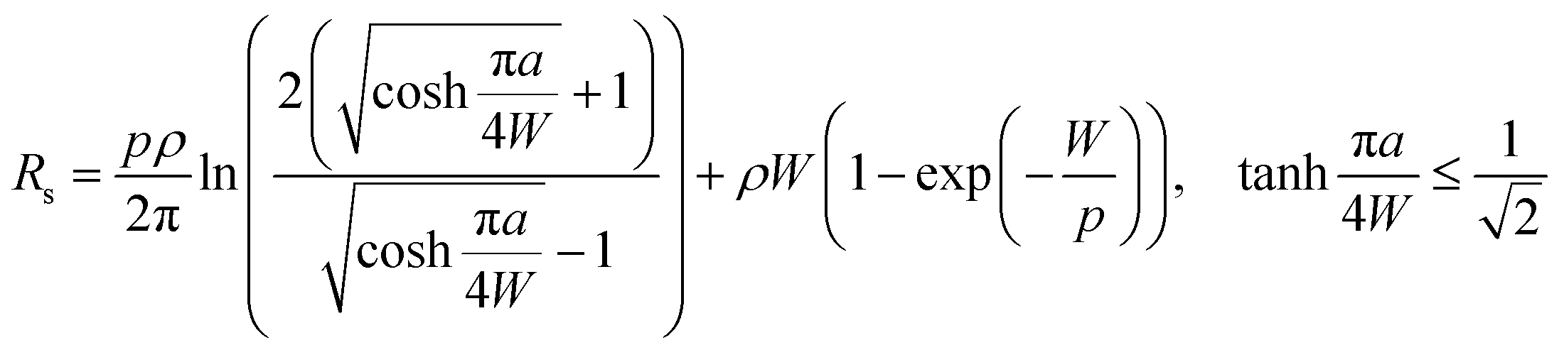
The Rs depends on the contact layout, and the metallization area fraction f. For line contacts, the metallization area fraction  depends on the line widths a and the contact pitches p. The Rs is calculated according to ref. 37:
| |
 | (4) |
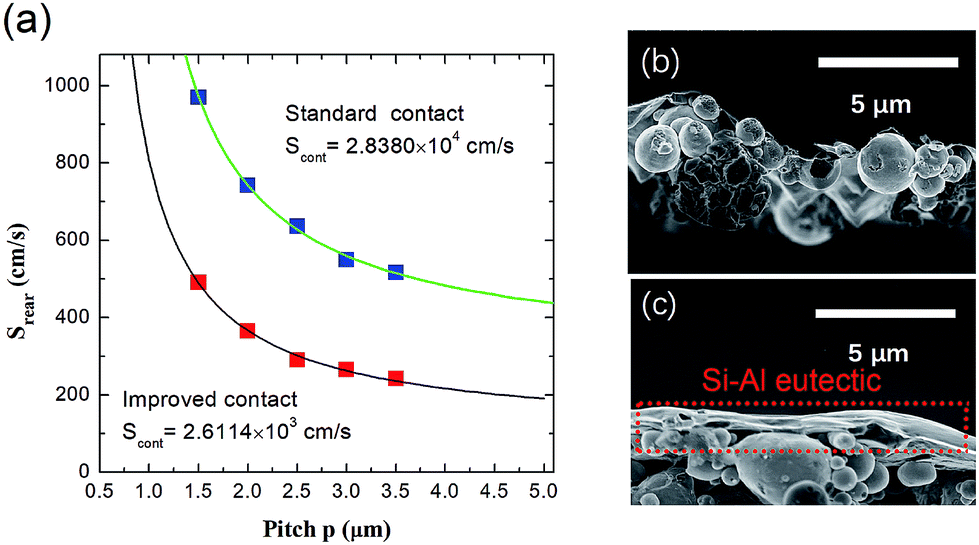
In Fig. 9(a), the dependence of Srear on the respective line pitch in each 25 × 25 mm2 area is shown. The red and blue solid squares are Srear calculated from experiments using eqn (2), the red and the blue curves are fitted results. Srear decreases with increasing line pitch due to the decrease in metallization fraction. Applying a SiO2 interface layer and improved Al-p+ conditions results in significantly much lower Srear values compared to that under the standard industrial condition. By fitting experimental results using eqn (3) and (4), we extract Smet = 2.8380 × 104 cm s−1 for the conventional screen-printed standard contacts and Smet = 2.6114 × 103 cm s−1 for the improved contacts. To understand the change in Scont measured at the two contacts, we investigate the formation of the Al-p+ layer beneath the contacts by means of SEM. The SEM images of contact cross sections are shown in Fig. 9(b) and (c). Analyzing cross-sectional images, the most noticeable finding is a considerably thickened eutectic layer at the interface of Si–Al for the improved contacts. The significant decrease in Smet is attributed to the homogeneous Al-p+ region and the thick Si–Al eutectic formation over the entire contact, as indicated by the red dot square in Fig. 9(c). In contrast, the Si–Al interface using the standard method exhibits inadequate contact between the Si bulk and the metal, no continuous Si–Al eutectic is observed in Fig. 9(b).
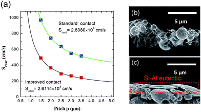 |
| | Fig. 9 (a) Effective rear-surface recombination velocity Srear as a function of line pitch p measured from the samples in (b) and (c). The square symbols correspond to experimental results for contacts prepared by the standard method (blue) and improved method (red). The green and black lines show the fits of the analytical model to the measured data. (b) and (c) SEM images of Si–Al interface of contacts prepared by the standard and improved methods, respectively. | |
3.5 Determination of the specific resistance
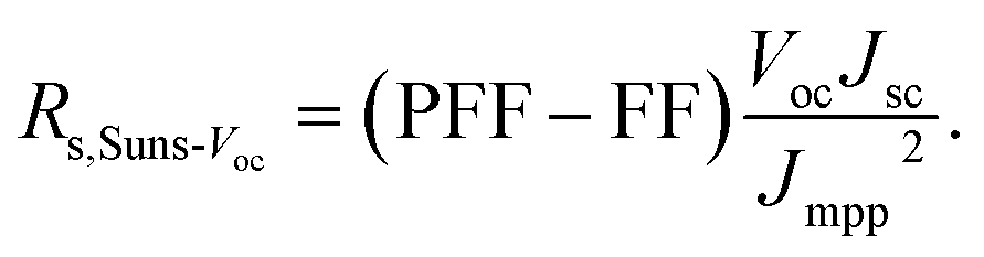
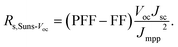
In order to achieve good electrical properties of solar cells, one of the primary conditions is to form a low-resistance ohmic contact between Si and Al. To study series resistance in our solar cells, their interface influence is tested by Suns-Voc measurements38 and light I–V measurements. The cells structures under test are shown in Fig. 10. According to eqn (5), the difference between PFF and FF translates into a series resistance of Rs,Suns-Voc39,40| |
 | (5) |
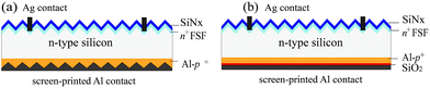 |
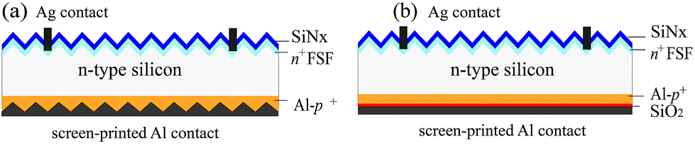
| | Fig. 10 Schematic of n-type solar cells. The rear Al-p+ emitters are alloyed from screen-printed pastes. (a) Standard solar cell with SiNx FSF passivation and pyramidally textured rear surface. (b) Improved solar cell with SiNx FSF passivation, polished rear surface, optimized Al emitter and interfacial oxide layer. | |
The FF is the fill factor from I–V curves and PFF is the pseudo fill factor from Suns-Voc curve, Jsc and Jmpp are short-circuit current density and current density at the maximum power point, respectively. It is calculated to be 0.94 ± 0.28 mΩ for the improved samples and 2.12 ± 0.71 mΩ for the standard samples. A decrease of 1.18 mW is realized. The smaller Rs,Suns-Voc values of group 2 cells is due to the thickened and uniform Si–Al alloy layer, which enables better transport of the majority carriers.
3.6 Solar cells
We applied the improved Al emitter to the 156 × 156 mm2 large-area back junction solar cells. The schematic solar cell structures are shown in Fig. 10. The standard solar cells (group 1) were fabricated using the industrial process for reference purposes. We notice that the height of the pyramids on the rear surface cannot be compensated even printing more Al, because the thick Al pastes are not able to completely reach pyramid bottom. For the solar cells in the improved process (group 2), a SiO2 ultra-thin layer is applied to the Si–Al interface at the rear side and the corresponding optimized annealing condition is used. The influence of the polished rear surface has been studied in our previous work.7 Compared with the cells featuring a polished rear surface without an interfacial layer, further improvements in the electronic parameters due to the SiO2 layer was evidenced.
Table 1 shows the I–V characteristic data of both cell types. An important finding is that the application of the ultra-thin SiO2 layer does not hinder the majority charge carrier transport across its barrier and thus allows for good FF of 79.82% and pFF of 80.6%. The reduced Rs and Rs,Suns-Voc for group 2 again stress the importance of the formation of a thick continuous eutectic at the rear contacts. As expected, the average Voc of the solar cells with optimized emitters is greatly increased to 636.03 mV, and Jsc is increased to 36.96 mA cm−2. The positive consequences are also apparent from the internal quantum efficiency (IQE) measurement which is shown in Fig. 11. A remarkable high response in the whole spectrum range is observed. We observe slightly lower IQE at short wavelengths for the optimized solar cell, the reason might lie in that the post-annealing process caused damage to the SiNx FSF passivation layers. However, better responses in long wavelength are clearly due to the optimized Al-p+ region, reduced recombination on the rear surface and in the emitter. The improvement in absolute efficiency is 2.18%, resulting in a 19.16% efficient, fully screen-printed solar cell when compared with solar cells fabricated by the conventional screen-printed process.
Table 1 Solar cell parameters measured under standard testing conditions (AM1.5, 1000 W m−2, 25 °C). The average values are calculated from 4–10 cells
| Cell groups |
Voc (mV) |
Jsc (mA cm−2) |
Rs (mΩ) |
FF (%) |
Eff. (%) |
PFF (%) |
Rs,Suns-Voc (mΩ) |
| 1 Average |
623.20 ± 9.85 |
35.97 ± 0.53 |
3.00 ± 1.78 |
72.71 ± 3.02 |
16.32 ± 1.09 |
80.13 ± 1.03 |
2.12 ± 0.71 |
| Best |
633.30 |
36.60 |
1.96 |
74.69 |
17.32 |
80.60 |
1.92 |
| 2 Average |
636.03 ± 1.02 |
36.96 ± 0.31 |
1.05 ± 0.47 |
78.68 ± 1.31 |
18.50 ± 0.41 |
82.55 ± 0.35 |
0.94 ± 0.28 |
| Best |
637.47 |
37.59 |
0.59 |
79.95 |
19.16 |
82.20 |
0.46 |
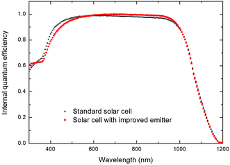 |
| | Fig. 11 Internal quantum efficiency curves of the standard solar cell and the solar cell with an optimized emitter. | |
4 Conclusion
Al emitters and contacts realized by full-area screen-printing of an Al paste have been intensively investigated. In order to form an optimal Al-p+ region for solar cells, an ultra-thin SiO2 layer at the interface of the metal and silicon was proposed and post-annealing treatments were adopted. A combination of experimental results and model calculations have been used to provide an understanding of the recombination effects in emitter and contacts, the transport properties, and the trends to choose optimal process conditions. It has been shown that the oxide layer acts as a barrier layer, migrating the inhomogeneity of the Al-p+ layer, and improving the morphology around rear contacts. As a result, recombination at the Si–Al interface, in the emitter and around contacts is significantly reduced. We further applied the improved emitters to large-area n-type industrial solar cells (156 × 156 mm2) with a full-area Al screen-printed rear emitter, gains of average efficiency by 2.18%, the Voc by 12.82 mV, the FF by 5.97% and the Jsc by 0.99 mA cm−2 were obtained. An optimal cell with an efficiency of 19.16%, Voc 637.47 mV was achieved. Further improvements in cell performance can still be expected if the annealing process is conducted in ambient N2, and by thickness optimization of SiO2.
Conflicts of interest
There are no conflicts to declare.
Acknowledgements
The authors would like to thank Solargiga Energy Holdings Ltd. for providing n-type Cz silicon wafers. This work has been partially funded by the National Natural Science Foundation of China (No. 61704018, 11574040 and 51661135021), the Doctoral Scientific Research Foundation of Liaoning Province No. 201501180 and SRF for ROCS, SEM.
Notes and references
- H. Hannebauer, T. Dullweber, U. Baumann, T. Falcon and R. Brendel, Phys. Status Solidi RRL, 2014, 8, 675–679 CrossRef CAS.
- N. Wehmeier, A. Nowack, B. Lim, T. Brendemühl, S. Kajari-Schröder, J. Schmidt, R. Brendel and T. Dullweber, Sol. Energy Mater. Sol. Cells, 2016, 158, 50–54 CrossRef CAS.
- J. Chen, J. Deckers, P. Choulat, I. Kuzma-Filipek, M. Aleman, A. U. De Castro, Z. R. Du, F. Duerinckx, B. Hoex, J. Szlufcik, J. Poortmans and A. G. Aberle, Prog. Photovoltaics Res. Appl., 2015, 23, 1706–1714 CrossRef CAS.
- J. Szlufcik, S. Sivoththaman, J. F. Nijs, R. P. Mertens and R. V. Overstraeten, in McEvoy’s Handbook of Photovoltaics, ed. S. A. Kalogirou, Academic Press, 3rd edn, 2018, pp. 129–158 Search PubMed.
- M. T. Zarmai, N. N. Ekere, C. F. Oduoza and E. H. Amalu, Appl. Energy, 2015, 154, 173–182 CrossRef CAS.
- M. Rauer, C. Schmiga, M. Glatthaar and S. W. Glunz, Sol. Energy Mater. Sol. Cells, 2018, 176, 295–301 CrossRef CAS.
- Y. Wei, P. Li, Y. Wang, X. Tan, C. Song, C. Lu, Z. Zhao and A. Liu, Sol. Energy, 2015, 118, 384–389 CrossRef CAS.
- M. A. Green, Sol. Energy, 2003, 74, 181–192 CrossRef CAS.
- S. Singh, F. Dross, N. E. Posthuma and R. Mertens, Sol. Energy Mater. Sol. Cells, 2011, 95, 1151–1156 CrossRef CAS.
- A. Moehlecke, F. S. Febras and I. Zanesco, Sol. Energy, 2013, 96, 253–262 CrossRef CAS.
- C. Gong, S. Singh, J. Robbelein, N. Posthuma, E. Van Kerschaver, J. Poortmans and R. Mertens, Prog. Photovoltaics Res. Appl., 2011, 19, 781–786 CrossRef CAS.
- R. Woehl, J. Krause, F. Granek and D. Biro, IEEE Electron Device Lett., 2011, 32, 345–347 CAS.
- X. Xi, X. Chen, S. Zhang, Z. Shi and G. Li, Appl. Surf. Sci., 2015, 339, 116–121 CrossRef CAS.
- F. Huster and Others, Proceedings of the 20th European Photovoltaic Solar Energy Conference, 2005, pp. 1466–1469 Search PubMed.
- T. Yoshikawa and K. Morita, J. Electrochem. Soc., 2003, 150, G465 CrossRef CAS.
- O. Krause, H. Ryssel and P. Pichler, J. Appl. Phys., 2002, 91, 5645 CrossRef CAS.
- M. Rauer, C. Schmiga, J. Krause, R. Woehl, M. Hermle and S. W. Glunz, Energy Procedia, 2011, 8, 200–206 CrossRef CAS.
- J. Krause, R. Woehl, M. Rauer, C. Schmiga, J. Wilde and D. Biro, Sol. Energy Mater. Sol. Cells, 2011, 95, 2151–2160 CrossRef CAS.
- R. Bock, P. P. Altermatt, J. Schmidt and R. Brendel, Semicond. Sci. Technol., 2010, 25, 105007 CrossRef.
- P. A. Basore and B. R. Hansen, IEEE Conference on Photovoltaic Specialists, 1990, vol. 1, pp. 374–379 Search PubMed.
- V. Meemongkolkiat, K. Nakayashiki, D. S. Kim, R. Kopecek and A. Rohatgi, J. Electrochem. Soc., 2006, 153, G53 CrossRef CAS.
- G. Huster and F. Schubert, Proceedings of the 20th European Photovoltaic Solar Energy Conference, 2005, pp. 1462–1465 Search PubMed.
- P. Li, Y. Wei, Z. Zhao, X. Tan, J. Bian, Y. Wang, C. Lu and A. Liu, Appl. Surf. Sci., 2015, 357, 1830–1835 CrossRef CAS.
- D. E. Kane and R. M. Swanson, IEEE photovoltaic specialists conference, 1985, pp. 578–583 Search PubMed.
- R. Woehl, P. Gundel, J. Krause, K. Ruhle, F. D. Heinz, M. Rauer, C. Schmiga, M. C. Schubert, W. Warta and D. Biro, IEEE Trans. Electron Devices, 2011, 58, 441–447 CAS.
- T. Mankad, R. A. Sinton, J. Swirhun and A. Blum, Energy Procedia, 2013, 38, 137–146 CrossRef CAS.
- Z. Zhao, P. Li, Y. Wei, C. Lu, X. Tan and A. Liu, Sol. Energy, 2014, 110, 714–719 CrossRef CAS.
- C. Mader, R. Bock, J. Schmidt and R. Brendel, Sol. Energy Mater. Sol. Cells, 2011, 95, 1720–1722 CrossRef CAS.
- M. Rüdiger, M. Rauer, C. Schmiga and M. Hermle, J. Appl. Phys., 2011, 110, 024508 CrossRef.
- H. Haug and J. Greulich, Energy Procedia, 2016, 92, 60–68 CrossRef CAS.
- J. Schmidt, N. Thiemann, R. Bock and R. Brendel, J. Appl. Phys., 2009, 106, 093707 CrossRef.
- J. Davis, a. Rohatgi, R. Hopkins, P. Blais, P. Rai-Choudhury, J. McCormick and H. Mollenkopf, IEEE Trans. Electron Devices, 1980, 27, 677–687 Search PubMed.
- J. Müller, K. Bothe, S. Gatz, H. Plagwitz, G. Schubert and R. Brendel, IEEE Trans. Electron Devices, 2011, 58, 3239–3245 Search PubMed.
- J. Müller, K. Bothe, S. Gatz, H. Plagwitz, G. Schubert and R. Brendel, Energy Procedia, 2011, 8, 337–342 CrossRef.
- A. B. Sproul, J. Appl. Phys., 1994, 76, 2851–2854 CrossRef CAS.
- B. Fischer, Ph.D. thesis, Universität Konstanz, Fachbereich Physik Konstanz, March 2003.
- H. Plagwitz, Ph.D. dissertation, Univ. Hanover, 2007.
- R. A. Sinton and A. Cuevas, Appl. Phys. Lett., 1996, 69, 2510 CrossRef CAS.
- F. Feldmann, M. Bivour, C. Reichel, M. Hermle and S. W. Glunz, Sol. Energy Mater. Sol. Cells, 2014, 120, 270–274 CrossRef CAS.
- D. Pysch, A. Mette and S. W. Glunz, Sol. Energy Mater. Sol. Cells, 2007, 91, 1698–1706 CrossRef CAS.
|
| This journal is © The Royal Society of Chemistry 2019 |
Click here to see how this site uses Cookies. View our privacy policy here. 
 Open Access Article
 This Open Access Article is licensed under a Creative Commons Attribution-Non Commercial 3.0 Unported Licence
 *a,
Xue Jiang
*a,
Xue Jiang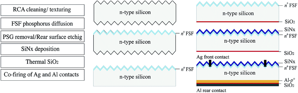

 curve shows a linear dependence of Δn, which can be used to extract j0,total. For our asymmetric samples, the saturation current density of the Al emitter (j0,Al) can be extracted by j0,Al = j0,total − j0,residual. The saturation current density of samples without Al-p+ region (j0,residual) can be determined with the help of an additional symmetric reference. The j0,Al for the sample with SiO2 and treated under 500 °C for 30 min is found to be 209.5 ± 44.5 fA cm−2, exhibiting a marked decrease of 1.54 pA cm−2 compared with the standard processed sample.
 depends on the line widths a and the contact pitches p. The Rs is calculated according to ref. 37: