
 Open Access Article
 This Open Access Article is licensed under a Creative Commons Attribution-Non Commercial 3.0 Unported Licence
Hydrothermal synthesis of MoS2 nanosheet loaded TiO2 nanoarrays for enhanced visible light photocatalytic applications
Miao Zhang acd,
Shun Wangb,
Ziliang Lia,
Chunwang Liua,
Rui Miaob,
Gang Heac,
Min Zhaobc,
Jun Xueb,
Zhiyuan Xiab,
Yongqi Wangb,
Zhaoqi Suna and
Jianguo Lv*bc
acd,
Shun Wangb,
Ziliang Lia,
Chunwang Liua,
Rui Miaob,
Gang Heac,
Min Zhaobc,
Jun Xueb,
Zhiyuan Xiab,
Yongqi Wangb,
Zhaoqi Suna and
Jianguo Lv*bc
aSchool of Physics and Materials Science, Anhui University, Hefei 230039, China
bSchool of Physics and Materials Engineering, Hefei Normal University, Hefei 230601, China. E-mail: lvjg1@163.com; Fax: +86 551 63674131; Tel: +86 551 63674132
cCo-operative Innovation Research Center for Weak Signal-Detecting Materials and Devices Integration, Anhui University, Hefei 230601, PR China
dKey Laboratory of Materials Physics, Institute of Solid State Physics, Chinese Academy of Sciences, Hefei, 230031, PR China
First published on 25th January 2019
Abstract
A molybdenum disulfide (MoS2) nanosheet-decorated titanium dioxide (TiO2) NRA heterojunction composite was fabricated successfully through a two-step hydrothermal approach. Microstructures and optical properties of specimens were characterized by field-emission scanning electron microscopy, X-ray diffractometry, X-ray photoelectron spectroscopy, and ultraviolet-visible spectroscopy. The gaps of the TiO2 nanorods have been filled with tiny MoS2 nanosheets, which can increase the surface area of MoS2/TiO2 NRA composite thin films. In addition, the photocatalytic activity of the thin films were measured and discussed in greater detail. The appropriate hydrothermal reaction temperature of MoS2 is important for the growth of perfect MoS2/TiO2 NRA composites with significantly enhanced photocatalytic performance. The photodegradation rate and k value of MoS2-220/TiO2 are 86% and 0.0105 min−1, respectively, which are much larger than those of blank TiO2. The enhanced photocatalytic performance could be attributed to the higher visible light absorption and the reduced recombination rate of photogenerated electron–hole pairs.
1. Introduction
In recent years, a large and growing literature has investigated the photocatalytic degradation and solar energy conversion to provide clean fuels1–3 for addressing the energy crisis and environmental pollution. Titanium dioxide (TiO2) as a semiconductor photocatalytic material has been broadly investigated due to its high photocatalytic activity, chemical stability, low cost and nontoxicity.4 In order to improve the photocatalytic activities, many efforts have been made for the fabrication of various morphologies of TiO2, such as hollow spheres, hierarchical microspheres, nanorods, nanotubes and porous networks.5–7 However, the fast recombination of photogenerated electron–hole pairs and large band gap (3.2 eV) of TiO2 limit the use of sunlight as well as photocatalytic activity. In order to overcome these drawbacks, rational designs of TiO2-based heterojunction photocatalysts with desirable architectural structure/morphology have been put into effect.8–11 It is well-known that two-dimensional MoS2 is a potential candidate for enhancing the visible light absorption and charge separation ability. Recently, MoS2/TiO2 heterostructures with diverse morphologies have been reported by researchers and have shown high photocatalytic activities in the visible light region.12–14 However, most of the MoS2/TiO2 heterostructures were powder materials, which were either difficult to recycle or would require additives in order to prepare the electrodes. In order to overcome these drawbacks, researchers made great efforts to prepare the film-based heterostructure composites with enhanced photocatalytic performances. Zheng et al.15 prepared the hierarchical MoS2 nanosheet@TiO2 nanotube arrays via anodization and hydrothermal methods. Photocatalytic activity of the compositing MoS2@TiO2 hybrids can be enhanced by means of appropriate modification of MoS2 on TiO2 nanotube arrays. To the best of our knowledge, the studies on the synthesis of MoS2 nanosheet coating on the TiO2 nanoarrays are limited.Herein, we demonstrate a facile two-step hydrothermal method to prepare MoS2/TiO2 NRA composite thin films with a highly-ordered three-dimensional hierarchical structure. The unique hierarchical structure of MoS2/TiO2 NRA heterojunctions was propitious to improve the light harvesting and charge separation rates. The novel MoS2/TiO2 NRAs exhibit enhanced photocatalytic activity due to the lower recombination rate and higher visible light absorption compared with the pure TiO2 NRAs.
2. Experimental
A simple two-step hydrothermal approach was adopted to prepare MoS2 nanosheet-loaded highly ordered TiO2 nanoarrays (NRAs). TiO2 NRAs were synthesized via the hydrothermal method. Then, 0.68 mL of tetrabutyl titanate was mixed with 20 mL of hydrochloric acid and 20 mL of deionized water (DI water). The mixed solution was magnetically stirred for 30 min and transferred into a 50 mL Teflon-lined stainless steel autoclave. Subsequently, a clean FTO glass was placed vertically in the autoclave, which was heated at 150 °C for 10 hours and then cooled to room temperature. The obtained TiO2 NRAs were washed thoroughly with DI water and dried at 60 °C for several hours.The preparation procedure of the MoS2/TiO2 NRA composite thin film is depicted as follows. 0.12 g thioacetamide (C2H5NS) and 0.06 g sodium molybdate (Na2MoO4·2H2O) were dissolved in 40 mL DI water and magnetically stirred for 30 min to form a transparent solution. The mixed solution was transferred into a 50 mL-Teflon-lined stainless steel autoclave. The TiO2 NRAs were placed vertically in the autoclave, which was heated at 200 °C and 220 °C for 24 h. The MoS2/TiO2 NRA composite thin film was obtained after washing the product with DI water and drying at 60 °C for 12 h.
Field-emission scanning electron microscopy (FE-SEM, S-4800) was adopted to observe the topologies of the samples. An X-ray diffractometer (XRD) was used to record the diffraction patterns of the samples. Chemical compositions of the samples were analyzed via X-ray photoelectron spectroscopy (XPS, ESCALAB 250). The structural properties of the samples were examined using a laser micro-Raman spectrometer (Renishaw in Via-Reflex) at an excitation wavelength of 532 nm. Optical properties of the samples were characterized by an ultraviolet-visible spectrophotometer (UV-2550, Shimadzu). The photocatalytic performances of the samples were estimated by the degradation of methylene blue (MB) solution. A thin film (25 × 25 mm) was placed in a glass culture dish containing 10 mL MB solution (5 ppm), which was chosen as the simulated contaminant. Then, the glass culture dish was placed under the visible-light irradiation from a Xenon lamp with a 420 nm cut-off filter. The photocatalytic performance can be estimated by comparing the absorbance of MB at a certain light irradiation with that of the initial MB solution at a characteristic wavelength of 664 nm.
3. Results and discussion
Fig. 1 presents the top-view FE-SEM images of TiO2 NRAs, MoS2-200/TiO2 and MoS2-220/TiO2 on an FTO substrate. As shown in the FE-SEM image in Fig. 1a, the TiO2 NRAs are well-aligned perpendicular to the FTO substrate. The nanorods have an average diameter of ∼100 nm. In MoS2-200/TiO2 (Fig. 1b), many tiny MoS2 nanosheets exist on the side and top facets of TiO2 nanorods. As the growth temperature of MoS2 increases to 220 °C, the gap of the TiO2 nanorods fills with tiny MoS2 nanosheets, which form the well-stacked layered structure of MoS2.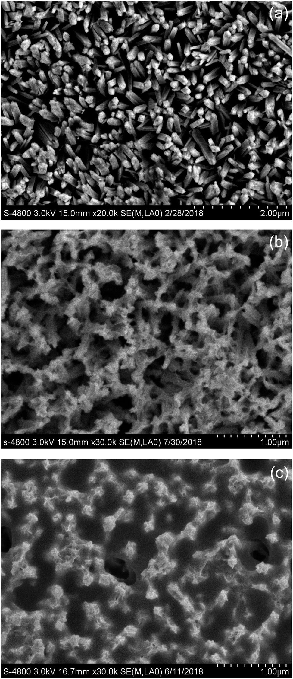 | ||
| Fig. 1 Top-view FE-SEM images of (a) TiO2 NRAs, (b) MoS2-200/TiO2, and (c) MoS2-220/TiO2. | ||
Fig. 2 presents the XRD patterns of TiO2 NRAs, MoS2-200/TiO2 and MoS2-220/TiO2. The diffraction peaks for the TiO2 NRAs match the standard peaks of rutile TiO2 phase (JCPDS card no. 65-0191) with the lattice parameters of a = b = 0.4593 nm and c = 0.2958 nm. Five characteristic peaks at 2θ = 36.08°, 54.33°, 62.77°, 69.01° and 69.82° can be respectively assigned to the (101), (211), (002), (301) and (112) crystal facets of rutile TiO2. With regard to MoS2/TiO2 NRA composite thin films, all diffraction peaks of the rutile TiO2 phase still exist in the XRD patterns. These results indicate that the TiO2 NRAs are well maintained in the hydrothermal process. Furthermore, the intensity of the diffraction peaks for rutile TiO2 of MoS2-200/TiO2 is stronger than that of rutile TiO2, which may be attributed to the recrystallization of rutile TiO2 in the second step of the hydrothermal process. The decrease in the diffraction peak intensities for TiO2 of MoS2-220/TiO2 may be due to the shielding effect of the large amounts of MoS2 loaded onto TiO2. No diffraction peak for MoS2 has been observed in MoS2-200/TiO2. Absence of the diffraction peak indicates that the modificatory MoS2 nanosheets on the TiO2 NRAs may only contain a spot of MoS2 nanosheets, which cannot be detected by XRD. Three characteristic peaks at 2θ = 14.40°, 33.52° and 58.35° have been observed in MoS2-220/TiO2, which can be indexed to (002), (101) and (110) crystal facets of MoS2 (JCPDS card no. 65-7025), respectively. The stronger (002) diffraction peak that appeared in the XRD pattern of the sample indicates the formation of a well-stacked layered structure of MoS2.16
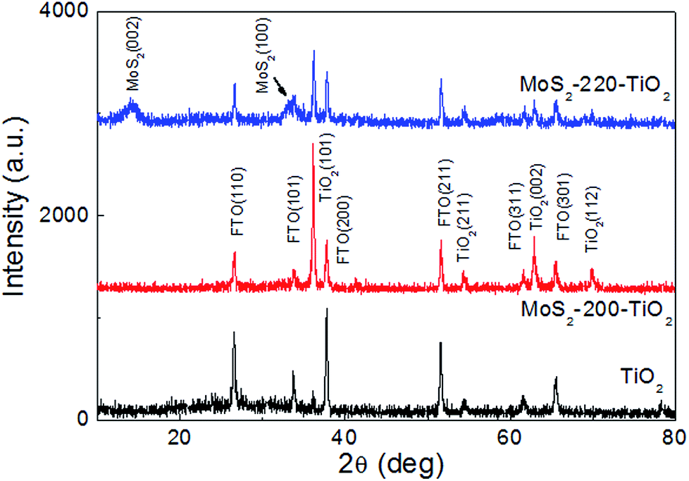 | ||
| Fig. 2 XRD patterns of TiO2 NRAs, MoS2-200/TiO2 and MoS2-220/TiO2. | ||
In order to obtain the detailed topography of the binary composite thin film, TEM images of the MoS2-220/TiO2 composites have been recorded. Fig. 3a and b represent the typical transmission electron microscopy (TEM) images of the MoS2-220/TiO2 composite. It can be seen that the tiny MoS2 nanosheets cover the surface of TiO2 nanorods. Fig. 3c shows the high-resolution transmission electron microscopy (HRTEM) image of the composite thin film. The lattice fringes that are perpendicular to the growth direction have a lattice spacing of 0.32 nm, which is equal to the lattice parameter in the (110) facet of the rutile TiO2. The lattice spacing is 0.62 nm, which corresponds to the (002) plane of MoS2.
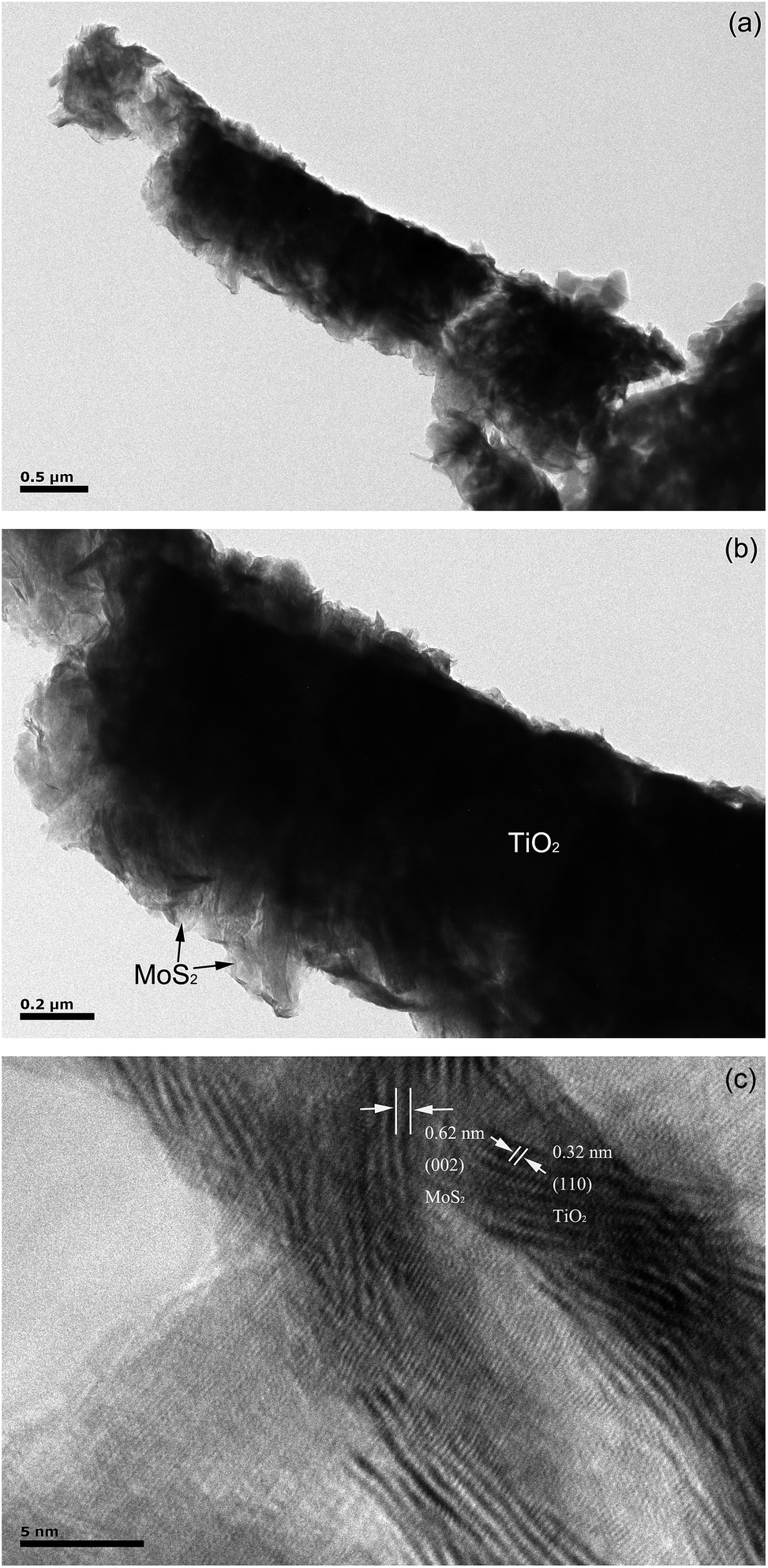 | ||
| Fig. 3 (a and b) TEM images of MoS2-220/TiO2 composites. (c) High-resolution TEM (HRTEM) images of pristine TiO2 NRAs. | ||
As shown in Fig. 4, the survey XPS spectra show that the dominant elements in MoS2-220/TiO2 are Ti, O, S, Mo, and C (Fig. 4a). The high-resolution XPS spectra of Mo and S for MoS2-220/TiO2 are shown in Fig. 4b and c. The binding energies at 232.2 and 229.0 eV with a separation energy close to 3.2 eV are ascribed to the Mo3d3/2 and Mo3d5/2 of the Mo element in the tetravalent state.17 In addition, the binding energy at 235.9 eV is ascribed to the Mo(3d3/2) signal of the Mo element in the hexavalent state, which results from the partial surface oxidation of MoS2 in air.16 As shown in Fig. 4c, the S2p spectrum can be deconvoluted into two peaks. The binding energies at 163.3 and 161.9 eV are attributed to the S(2p1/2) and S(2p3/2) signals, respectively, of sulphide element in the divalent state. As shown in Fig. 4d, the C1s spectrum can be deconvoluted into three peaks, which correspond to C![[double bond, length as m-dash]](https://www.rsc.org/images/entities/char_e001.gif) O (288.4 eV), C–O (286.4 eV), and C–C (284.8 eV), respectively.18 As shown in Fig. 4e, the spin-energy separation between Ti2p1/2 (464.3 eV) and Ti2p3/2 (458.5 eV) peaks is about 5.8 eV, which is assigned to the Ti4+ state in the pure TiO2 NRAs.19 The binding energies of Ti2p1/2 (465.0 eV) and Ti2p3/2 (459.2 eV) for MoS2-220/TiO2 shift to higher energies because of the existence of Ti3+ states by trapping electrons,16 which exhibit higher activity and form the radicals covalently on the surface of TiO2. These trapped charge carriers can be transferred to the conduction or valence band by thermal excitation, which is beneficial to enhance the photocatalytic abilities.20
O (288.4 eV), C–O (286.4 eV), and C–C (284.8 eV), respectively.18 As shown in Fig. 4e, the spin-energy separation between Ti2p1/2 (464.3 eV) and Ti2p3/2 (458.5 eV) peaks is about 5.8 eV, which is assigned to the Ti4+ state in the pure TiO2 NRAs.19 The binding energies of Ti2p1/2 (465.0 eV) and Ti2p3/2 (459.2 eV) for MoS2-220/TiO2 shift to higher energies because of the existence of Ti3+ states by trapping electrons,16 which exhibit higher activity and form the radicals covalently on the surface of TiO2. These trapped charge carriers can be transferred to the conduction or valence band by thermal excitation, which is beneficial to enhance the photocatalytic abilities.20
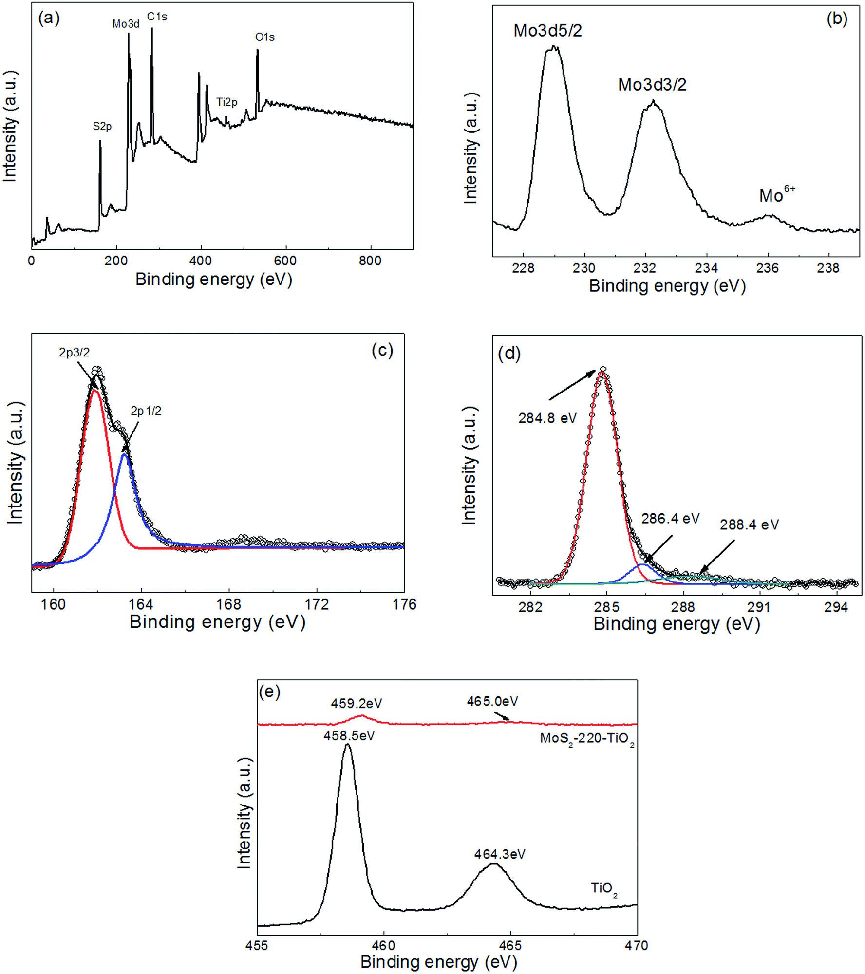 | ||
| Fig. 4 XPS survey spectra of (a) MoS2-220/TiO2, (b) Mo3d, (c) S2p, (d) C1s, and (e) Ti2p. | ||
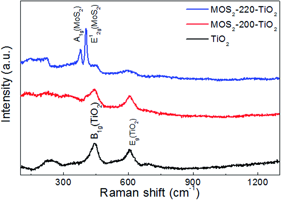
Fig. 5 shows the Raman spectra of TiO2 NRAs, MoS2-200/TiO2 and MoS2-220/TiO2. It can be seen from the Raman curve of bare TiO2 NRAs that the two resonance peaks centered at 445 and 608 cm−1 can be attributed to the B1g and Eg of TiO2 with rutile phase, respectively.21 There are three resonance peaks centered at 404, 445 and 608 cm−1, which can be observed from MoS2-200/TiO2, which may be attributed to the out-of-plane E2g1 of MoS2 and the B1g and Eg of TiO2, respectively.22 These results indicate that a spot of MoS2 nanosheets deposited on the TiO2 NRAs. The Raman curve of MoS2-220/TiO2 shows two strong resonance peaks centered at 375 and 404 cm−1, which may be ascribed to in-plane A1g and out-of-plane E2g1 of MoS2, respectively. The other two weak resonance peaks centered at 445 and 608 cm−1 may be assigned to B1g and Eg of TiO2, respectively, which weakened with the increase in MoS2 nanosheet content.
 | ||
| Fig. 5 Raman spectra of TiO2 NRAs, MoS2-200/TiO2 and MoS2-220/TiO2. | ||
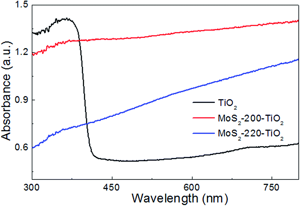
Fig. 6 shows the UV-vis absorption spectra of TiO2 NRAs, MoS2-200/TiO2 and MoS2-220/TiO2. It can be seen that the spectrum of TiO2 NRAs shows an abrupt absorption edge at about 400 nm and strong absorption in UV region. For MoS2-200/TiO2 and MoS2-220/TiO2, absorbance in the visible region has been enhanced due to the visible light absorbance arising from MoS2, which possesses the considerably narrowed band gap. These results indicated that the TiO2 NRAs were successfully modified by MoS2 nanosheets. The enhanced visible light absorbance of MoS2/TiO2 can improve the visible photocatalytic activity of the samples.21 It can also be seen that the UV absorption is greatly dependent on the amount of MoS2 loaded onto TiO2. This may be attributed to the shielding effect of MoS2 on TiO2, which reduces the UV absorption of TiO2.23
 | ||
| Fig. 6 UV-vis absorbance spectra of TiO2 NRAs, MoS2-200/TiO2 and MoS2-220/TiO2. | ||
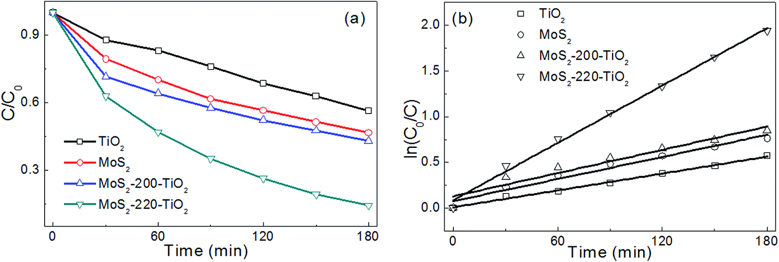
The photocatalytic performances of TiO2 NRAs, MoS2, MoS2-200/TiO2 and MoS2-220/TiO2 were estimated by means of the photodegradation of MB under visible light. Fig. 7a shows the photodegradation rate of the samples. It is evident that the photodegradation rate of MoS2-220/TiO2 is far greater than that of TiO2 NRAs, MoS2, and MoS2-200/TiO2. The photodegradation rate of TiO2 NRAs, MoS2, MoS2-200/TiO2 and MoS2-220/TiO2 is about 44%, 53%, 57% and 86%, respectively, after visible light irradiation for 180 min.
 | ||
| Fig. 7 (a) Normalized absorption of MB in the presence of TiO2 NRAs, MoS2-200/TiO2 and MoS2-220/TiO2 under visible light irradiation. (b) The plots of ln(C0/C) versus t of TiO2 NRAs, MoS2-200/TiO2 and MoS2-220/TiO2. | ||
The photodegradation of MB solution follows the pseudo-first-order reaction and its kinetics can be expressed as follows:17
| ln(C0/C) = kt | (1) |
For the as-deposited TiO2 NRAs, the photocatalytic degradation under visible light irradiation may be attributed to the existence of abundant defects, which will induce defect levels and narrow band-gaps and then improve the visible light absorption.24 The schematic of the energy band structure and separation principle of carriers in MoS2-220/TiO2 is shown in Fig. 8. First, a small amount of electrons can be excited from the defect levels (or valence band) to the conduction band when TiO2 is illuminated by visible light. Second, it is well known that MoS2 is a narrow bandgap semiconductor with a band gap of about 1.8 eV. Upon visible light illumination, the electrons in the valence band (VB) of MoS2 can be excited to conduction band (CB), thus leaving holes in the VB. As the CB of TiO2 is lower than that of MoS2, the photogenerated electrons in the CB of MoS2 can be transferred to the CB of TiO2 NRAs.17 TiO2 is considered to be an electron receiver, which is conducive to the separation of charge carriers. The electrons may be captured by oxygen (O2) to form superoxide radical anions (˙O2−), which can react with a simulated pollutant. In addition, the holes left in the VB of MoS2 can react with H2O to form hydroxyl radicals, which can react with the dye on the sample.25 Therefore, the electron and hole can be separated efficiently through the formation of a heterojunction between MoS2 and TiO2. Finally, the photocatalytic activities of MoS2/TiO2 could be enhanced by introducing MoS2 onto the TiO2 NRAs.
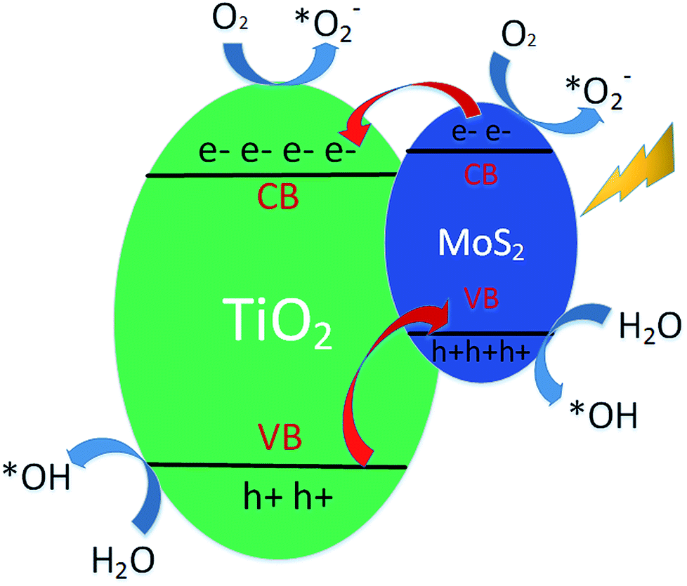 | ||
| Fig. 8 Schematic of the energy band structure and separation principle of carriers in MoS2-220/TiO2. | ||
4. Conclusions
A novel MoS2 nanosheet decorating TiO2 NRA heterojunction composite with outstanding photocatalytic performance for the degradation of organic pollutants under visible light illumination was deposited by a hydrothermal method on the FTO substrate. SEM, XRD and Raman results confirmed that MoS2 nanosheets loaded on the surface of the TiO2 NRAs and filled the gap between TiO2 nanorods. Energy band structure of the MoS2-220/TiO2 heterojunction composite could promote charge transfer and prevent the recombination of photogenerated electron–hole pairs. The MoS2-220/TiO2 heterojunction composite exhibits the best photocatalytic activity, and the photodegradation rate and k value are 86% and 0.0105 min−1, respectively.Conflicts of interest
There are no conflicts to declare.Acknowledgements
This study was supported by the National Natural Science Foundation of China (no. 51701001, 51102072, 51472003, and 51572002), Natural Science Foundation of Anhui Higher Education Institution of China (no. KJ2015ZD32, KJ2017A924, and KJ2017A002), Doctor Scientific Research Fund of Anhui University (no. J01001927), Youth Core Teacher Fund of Anhui University (no. J01005111), Foundation of Co-operative Innovation Research Center for Weak Signal-Detecting Materials and Devices Integration Anhui University (no. Y01008411, and WRXH201703), and the Key Laboratory of Materials Physics, Institute of Solid State Physics, Chinese Academy of Sciences (no. 2016KLMP01).References
- J. Dong, X. Zhang, J. Huang, S. Gao, J. Mao, J. Cai, Z. Chen, S. Sathasivam, C. J. Carmalt and Y. Lai, Boosting heterojunction interaction in electrochemical construction of MoS2 quantum dots@TiO2 nanotube arrays for highly effective photoelectrochemical performance and electrocatalytic hydrogen evolution, Electrochem. Commun., 2018, 93, 152–157 CrossRef CAS.
- M. D. Patel, J. Zhang, J. Park, N. Choudhary, J. M. Tour and W. Choi, Directly deposited porous two-dimensional MoS2 films as electrocatalysts for hydrogen evolution reactions, Mater. Lett., 2018, 225, 65–68 CrossRef CAS.
- L. Yang, C. Xu, F. Wan, H. He, H. Gu and J. Xiong, Synthesis of RGO/BiOI/ZnO composites with efficient photocatalytic reduction of aqueous Cr(VI) under visible-light irradiation, Mater. Res. Bull., 2019, 112, 154–158 CrossRef CAS.
- C. Zhao, Y. Zhang, L. Chen, C. Yan, P. Zhang, M. A. Jia and X. Lu, Self-Assembly-Assisted Facile Synthesis of MoS2-Based Hybrid Tubular Nanostructures for Efficient Bifunctional Electrocatalysis, ACS Appl. Mater. Interfaces, 2018, 10, 23731 CrossRef CAS PubMed.
- X. Lei, K. Yu, H. Li and Z. Zhu, A functional design and synthesization for electrocatalytic hydrogen evolution material on MoS2/Co3S4 hybrid hollow nanostructure, Electrochim. Acta, 2018, 269, 262–273 CrossRef CAS.
- L. Xu and S. Wang, A novel hierarchical MoS2-ZnO-Ni electrocatalyst prepared by electrodeposition coupling with dealloying for hydrogen evolution reaction, J. Electroanal. Chem., 2018, 808, 173–179 CrossRef CAS.
- W. Zhang, Z. Xie, X. Wu, M. Sun, X. Deng, C. Liu, Z. Liu and Q. Huang, Acid-engineered defective MoS2 as an efficient electrocatalyst for hydrogen evolution reaction, Mater. Lett., 2018, 230, 232–235 CrossRef CAS.
- Q. Xiong, X. Zhang, H. Wang, G. Liu, G. Wang, H. Zhang and H. Zhao, One-step synthesis of cobalt-doped MoS2 nanosheets as bifunctional electrocatalysts for overall water splitting under both acidic and alkaline conditions, Chem. Commun., 2018, 54, 3859–3862 RSC.
- Z. Chen, D. Cummins, B. N. Reinecke, E. Clark, M. K. Sunkara and T. F. Jaramillo, Core-shell MoO3-MoS2 Nanowires for Hydrogen Evolution: A Functional Design for Electrocatalytic Materials, Nano Lett., 2011, 11, 4168–4175 CrossRef CAS PubMed.
- J. Xie, H. Zhang, S. Li, R. Wang, X. Sun, M. Zhou, J. Zhou, X. W. Lou and Y. Xie, Defect-rich MoS2 ultrathin nanosheets with additional active edge sites for enhanced electrocatalytic hydrogen evolution, Adv. Mater., 2013, 25, 5807–5813 CrossRef CAS PubMed.
- L. Liu, C. Luo, J. Xiong, Z. Yang, Y. Zhang, Y. Cai and H. Gu, Reduced graphene oxide (rGO) decorated TiO2 microspheres for visible-light photocatalytic reduction of Cr(VI), J. Alloys Compd., 2017, 690, 771–776 CrossRef CAS.
- J. Kibsgaard, Z. Chen, B. N. Reinecke and T. F. Jaramillo, Engineering the surface structure of MoS2 to preferentially expose active edge sites for electrocatalysis, Nat. Mater., 2012, 11, 963–969 CrossRef CAS PubMed.
- J. Yang and H. Shin, Recent advances in layered transition metal dichalcogenides for hydrogen evolution reaction, J. Mater. Chem. A, 2014, 2, 5979–5985 RSC.
- R. Chianelli, M. Siadati, M. P. L. Rosa, G. Berhault, J. Wilcoxon, R. Bearden Jr and B. Abrams, Catalytic Properties of Single Layers of Transition Metal Sulfide Catalytic Materials, Catal. Rev., 2006, 48, 1–41 CrossRef CAS.
- L. Zheng, S. Han, H. Liu, P. Yu and X. Fang, Hierarchical MoS2 Nanosheet@TiO2 Nanotube Array Composites with Enhanced Photocatalytic and Photocurrent Performances, Small, 2016, 12, 1527–1536 CrossRef CAS PubMed.
- D. Qi, S. Li, Y. Chen and J. Huang, A hierarchical carbon@TiO2@MoS2 nanofibrous composite derived from cellulose substance as an anodic material for lithium-ion batteries, J. Alloys Compd., 2017, 728, 506–517 CrossRef CAS.
- C. Wang, W. Wan, Y. Huang, J. Chen, H. H. Zhou and X. X. Zhang, Hierarchical MoS2 nanosheet/active carbon fiber cloth as a binder-free and free-standing anode for lithium-ion batteries, Nanoscale, 2014, 6, 5351–5358 RSC.
- S.-K. Park, J. Lee, S. Bong, B. Jang, K.-d. Seong and Y. Piao, Scalable Synthesis of Few-Layer MoS2 Incorporated into Hierarchical Porous Carbon Nanosheets for High-Performance Li- and Na-Ion Battery Anodes, ACS Appl. Mater. Interfaces, 2016, 8, 19456–19465 CrossRef CAS PubMed.
- C. Ma, X. Wang, H. Luo and D. Zhang, Synthesis of Ag/TiO2 core–shell nanowires with enhanced stability of photocatalytic activity, J. Mater. Sci.: Mater. Electron., 2017, 28, 10715–10719 CrossRef CAS.
- P. Roy, S. Berger and P. Schmuki, TiO2 Nanotubes: Synthesis and Applications, Angew. Chem., Int. Ed., 2011, 50, 2904–2939 CrossRef CAS PubMed.
- F. Zhao, Y. Rong, J. Wan, Z. Hu, Z. Peng and B. Wang, MoS2 quantum dots@TiO2 nanotube composites with enhanced photoexcited charge separation and high-efficiency visible-light driven photocatalysis, Nanotechnology, 2018, 29, 105403 CrossRef PubMed.
- W. Jian, X. Cheng, Y. Huang, Y. You, R. Zhou, T. Sun and J. Xu, Arrays of ZnO/MoS2 nanocables and MoS2 nanotubes with phase engineering for bifunctional photoelectrochemical and electrochemical water splitting, Chem. Eng. J., 2017, 328, 474–483 CrossRef CAS.
- J. Low, J. Yu, M. Jaroniec, S. Wageh and A. A. Al-Ghamdi, Heterojunction Photocatalysts, Adv. Mater., 2017, 29, 1601694 CrossRef PubMed.
- Z. Wu, S. Cao, C. Zhang and L. Piao, Effects of bulk and surface defects on the photocatalytic performance of size-controlled TiO2 nanoparticles, Nanotechnology, 2017, 28, 275706 CrossRef PubMed.
- J. Lv, R. Miao, M. Zhang, G. He, M. Zhao, B. Yu, W. Wang, B. Li and Z. Sun, Few-layers MoS2 sensitized Ag-TiO2 nanocomposite thin film for enhancing photocatalytic activity, J. Mater. Sci.: Mater. Electron., 2018, 29, 16282–16288 CrossRef CAS.
| This journal is © The Royal Society of Chemistry 2019 |