
 Open Access Article
 This Open Access Article is licensed under a Creative Commons Attribution-Non Commercial 3.0 Unported Licence
Influence of cooling-induced edge morphology evolution during chemical vapor deposition on H2 etching of graphene domains†
Bin
Wang
 a,
Yuwei
Wang
b,
Guiqiang
Wang
a and
Qingguo
Zhang
*a
a,
Yuwei
Wang
b,
Guiqiang
Wang
a and
Qingguo
Zhang
*a
aCollege of New Energy, Bohai University, 19, Keji Rd., New Songshan District, Jinzhou City, Liaoning Province 121013, China. E-mail: wgqem@bhu.edu.cn
bDepartment of Chemistry and Environmental Sciences, Jinzhou Normal College, 189, Songpo Rd., Linghe District, Jinzhou City, Liaoning Province 121000, China
First published on 18th February 2019
Abstract
In this paper, we studied the influence of edge morphology evolution during the chemical vapor deposition cooling process on H2 etching of graphene domains. Hexagonal graphene domains were synthesized on a Cu substrate and etched with H2 at atmospheric pressure. After etching, two kinds of graphene edge morphologies were observed, which were closely associated with the cooling process. A visible curvature was observed at the graphene edges via an atomic force microscope, indicating that the graphene edges sank into the Cu surface during the cooling process, which protected the graphene edges from etching. This work demonstrates the changes in graphene edges during cooling and sheds light on the etching mechanism of graphene edges on a Cu substrate.
Introduction
Graphene as a 2D one-atom-thick sheet of carbon has drawn significant attention for future opto-electronic applications1–5 because of its novel properties.6,7 Excellent graphene-based photoelectric devices require graphene processing techniques, such as optimized synthesis methods,8–10 evolved etching techniques,11–13 and surface modifications.14 In terms of synthesis, graphene grown on a Cu substrate via chemical vapor deposition (CVD) has the distinct advantages of extremely large area, homogeneity, high quality, and monolayer graphene films.15–19The effects of CVD cooling on Cu-based graphene should not be neglected. A continuous CH4 flow during cooling influences the nucleation and the domain size of as-grown graphene.20 Mismatch in the thermal expansion coefficients of graphene and the Cu substrate causes the formation of wrinkles during cooling, which is revealed through H2 (ref. 21 and 22) and O2 etching of graphene.23 G. H. Han24 reported that the Cu surface is reconstructed and forms stripes during cooling, which are associated with graphene wrinkles.22 Lu et al. reported that the surface morphology of the Cu substrate changes with the cooling rate after graphene growth.25
However, information about the effects of cooling on the graphene edges is limited. In our present work, edge morphology evolution during CVD cooling was revealed though the H2 etching of graphene domains. The graphene edges sank into the Cu substrate during cooling. As a result, the cooling-induced edge evolution protected the graphene from edge etching until the etching temperature reached 1000 °C.
H2 etching is an effective method for investigating the growth mechanism of CVD graphene. The morphology and the distribution of wrinkles are clearly observed21,23 and a specific crystallographic edge is achieved via H2 etching.26,27 In this work, we revealed that differently etched morphologies of graphene domains depended on H2 etching conditions. In addition, the effect of CVD cooling on the graphene edge morphology evolution was emphasized though H2 etching.
Experimental
CVD graphene was synthesized by using a Cu foil (99.8%, 2 cm × 2 cm strips) as the substrate. Prior to the growth process, the Cu foil was electrochemically polished in H3PO4 to reduce the surface roughness. The Cu substrate was heated to 1050 °C with a flow of 1000 sccm Ar (purity, 99.999%) at atmospheric pressure and was annealed at 1050 °C for 60 min with 1000 sccm Ar and 200 sccm H2 (purity, 99.999%). After annealing, 1000 sccm Ar, 10 sccm H2, and 1 sccm dilute CH4 (mixed with Ar) were introduced to the CVD system for the graphene growth. The growth time was 40 min. After the growth, the samples were naturally cooled down to room temperature with a flow of 1000 sccm Ar. The thermal hydrogen etching conditions (time, temperature, and gas flow rate) for each sample are described in the corresponding section.Results and discussion
Hexagonal graphene domains were synthesized using a copper-catalyzed CVD method using Ar, H2, and Ar-diluted CH4 in a ratio of 1000![[thin space (1/6-em)]](https://www.rsc.org/images/entities/char_2009.gif) :10:1 at 1050 °C for 40 min. Fig. 1a shows the scanning electron microscopy (SEM) image of the synthesized hexagonal graphene domain. All hexagonal sides are straight, as shown by the red dotted line. Fig. 1b displays the Raman spectrum of the domain region A. The value of typical I2D was twice that of IG over the whole area within the graphene domain. A negligible D band signal was observed, indicating that the graphene domain was a single-layer graphene domain with low defect content. In the Raman spectrum of the domain edge B (Fig. 1c), pronounced ID was observed, which indicated high structural defect content on the domain edge.
:10:1 at 1050 °C for 40 min. Fig. 1a shows the scanning electron microscopy (SEM) image of the synthesized hexagonal graphene domain. All hexagonal sides are straight, as shown by the red dotted line. Fig. 1b displays the Raman spectrum of the domain region A. The value of typical I2D was twice that of IG over the whole area within the graphene domain. A negligible D band signal was observed, indicating that the graphene domain was a single-layer graphene domain with low defect content. In the Raman spectrum of the domain edge B (Fig. 1c), pronounced ID was observed, which indicated high structural defect content on the domain edge.
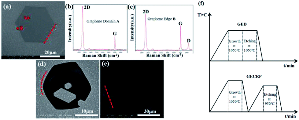 | ||
| Fig. 1 (a) SEM image of the synthesized hexagonal graphene domain. (b and c) Raman spectra of domain region A and edge B, respectively. (d) SEM image of the graphene domain etched directly after growth. (e) SEM image of the graphene domain etched after cooling and reheating. (f) Simple view of the growth and etching process of the two kinds of samples. | ||
Our H2 etching experiment on graphene domains was bifurcated. One was directly etched at 1050 °C for 30 min in the same chamber immediately after the growth process (Fig. 1d). The other one was naturally cooled to room temperature and reheated to 950 °C for 30 min to initiate H2 etching (Fig. 1e). The H2 etching was conducted with 2:5 H2–Ar gas flow rate (HAGFR) at atmospheric pressure. Fig. 1d presents the SEM image of graphene etched directly after the growth process (GED). A small amount of etched hexagons was observed on GED as a result of point defects.28 Some etched hexagons were enlarged to form a contiguous area. The straight domain edges were etched to an arc shape (please see the red dotted arc line in Fig. 1d), resulting in graphene with round shape and small size. Fig. 1e presents the SEM image of graphene etched after cooling and reheating (GECRP). Only a small amount of etched trenches was observed on the hexagonal graphene surface; these trenches were associated with the wrinkles formed on graphene during cooling to room temperature.21 The hexagonal shape was maintained over the full range of the domain size; the domain size did not change, and the hexagonal edges were still straight, as indicated by the red dotted line. This finding revealed that the graphene domain edges were not etched under this condition.
Fig. 1f shows a simple view of the growth and etching of the two kinds of graphene etching processes in our experiment. Given the different etching processes, GED displayed edge etching, a round shape, and etched hexagons inside. In contrast, GECRP maintained its shape and showed etched trenches. Thus, the different etching morphologies indicated that graphene has considerably evolved since cooling and reheating.
In addition, H2 etching was conducted on graphene domains with jagged edges (GDJE). This kind of graphene domain also underwent the cooling and reheating process. The etching condition was similar to that of GECRP. Fig. S1† shows that the etching trenches are also observed on the GDJE surface after etching, and the jagged edges are not etched away (the red dotted line region corresponds to the jagged edges), which indicate that edge etching is not related to the morphology of the edge.
The etched trench was caused by hydrogenation on the wrinkles formed during cooling. The density and the shape of wrinkles were associated with Cu crystal orientation.21 We conducted a verification experiment to determine whether the edge etching is also associated with the Cu crystal orientation. Fig. S2a† displays an optical microscopy image of the two types of etched trenches ((A) striated and (B) reticular) corresponding to different Cu crystal orientations. The etched trenches with different morphologies were observed via SEM images (Fig. S2b and c†). However, the etching from the edge was not observed. Thus, edge etching is independent of Cu crystal orientation.
We studied the influence of etching parameters such as time and temperature on the H2 etching degree of the graphene domain. The gas flow rate of etching did not change (200 sccm H2 and 500 sccm Ar).
First, a series of H2 etching was conducted on graphene at incremental time intervals of 30, 120, and 240 min with the etching temperature of 200 °C. The etching was random, and the etching trenches originally appeared to be narrow, as shown in the optical microscopy image in Fig. 2a. After prolonging the etching time to 120 min, we observed that the trenches exhibited minimal change (Fig. 2b). When the etching time was further increased to 240 min, the density and the width of trenches evidently increased compared with those of the trenches etched for 30 min (Fig. 2c).
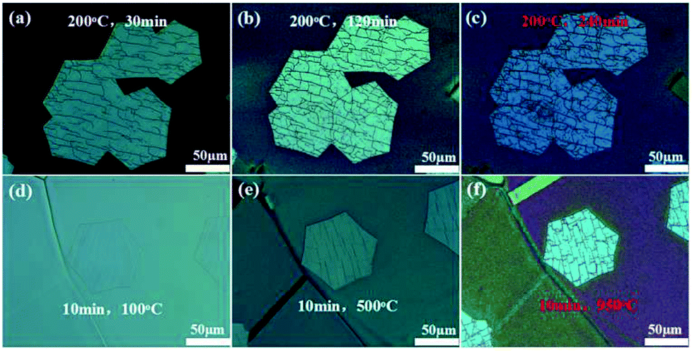 | ||
| Fig. 2 Optical microscopy images of graphene domains after etching. (a–c) Degree of etching depending on the etching times of 30, 120, and 240 min, respectively. The etching temperature was 200 °C. (d–f) Degree of etching depending on the etching temperatures of 100, 500, and 950 °C. The etching time was 10 min. The gas flow rate of etching was 2:5 (200 sccm H2 and 500 sccm Ar). | ||
Then, the effects of temperature on H2 etching of graphene were further investigated by increasing the etching temperature from 100 to 950 °C for 10 min. Initially, the etching trenches were not visible (etching temperature was 100 °C, Fig. 2d). When the temperature was increased to 500 °C, the etching trenches appeared and resulted in imperfections of the graphene surface (Fig. 2e). When the temperature was increased to 950 °C, the width of preceding trenches increased to a certain extent, and some other small trenches appeared (Fig. 2f). The etching degree for this etching condition (10 min, 950 °C) was similar to that for the previous condition (240 min, 200 °C). Thus, the etching temperature is a more significant factor for the H2 etching of graphene than the etching time. We concluded that edge etching mainly depends on the etching temperature.
We conducted a verification experiment to determine whether edge etching is associated with a higher etching temperature. After cooling down to room temperature, the as-grown graphene domains were reheated up to 1000 °C in Ar. The etching was performed with 20 sccm H2 and 500 sccm Ar for 10 and 15 min. Considering that the H2 etching of graphene was too fast to control at a temperature higher than 1000 °C with high HAGFR, the HAGFR from 2:5 to 2:50 and 1000 °C were selected as the etching conditions. Fig. 3a–c show the optical microscopy images of the etched graphene domains. The etching mode significantly changed. The graphene domains were etched from the wrinkles and edges. As shown in Fig. 3b, an individual graphene domain was inwardly etched to a distance of about ΔL, which was perpendicular to the corresponding edge, whereas the graphene edges remained straight. A few etched trenches were observed at the graphene surface. The same result was observed on coterminous graphene domains (Fig. 3a). All edges were inwardly etched with a uniform degree compared with the diversely etched trenches on the graphene surface. Fig. 3c shows the optical microscopy image of a graphene domain etched for 15 min. The edges were inwardly etched to a greater degree, which resulted in the formation of a graphene island. Compared with the etching morphologies of GECRP, the etched arc-shaped edges and the hexagonal openings inside were significantly observed in the optical microscopy image of GED (Fig. 3d). Fig. 3e and f exhibit the distinction of etching results between GECRP and GED with a schematic. For GECPR etched at 1000 °C, the inward etching was perpendicular to the corresponding edge with a uniform etching rate (indicated by the red arrows in Fig. 3e). Thus, the graphene domain maintained its hexagonal shape. On the contrary, the inward etching of GED was non-isotropic. The inward etching direction had a certain angular interval (indicated by the red arrows in Fig. 3f), and the etching rate of hexagonal angles was faster than that of the edges. As a result, the graphene domain was etched from a hexagonal shape to an oval shape. Thus, edge etching was associated with a higher etching temperature although the etching modes were distinguished.
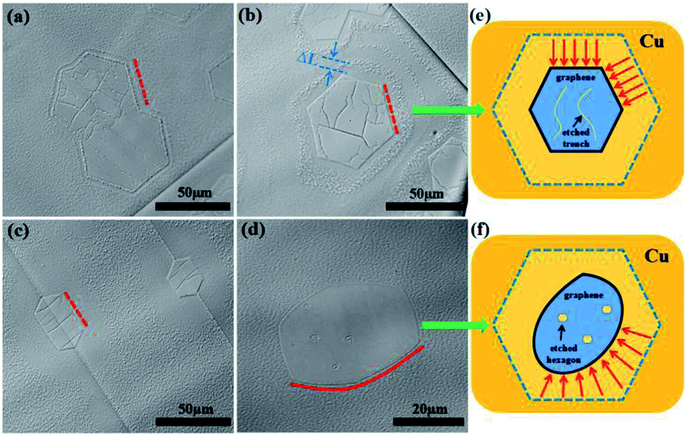 | ||
| Fig. 3 Optical microscopy images of graphene domains after etching at 1000 °C for (a and b) 10 and (c) 15 min. The gas flow rate of etching was 2:50 (20 sccm H2 and 500 sccm Ar). (d) Optical microscopy image of GED at 1050 °C. (e and f) Schematics of different etching results between GECRP and GED. | ||
AFM analysis was conducted to elucidate the evolution of the graphene edge after cooling. Fig. 4a displays the AFM image of a hexagonal graphene domain grown on a Cu substrate. The discernible brown hexagon indicated that the graphene edges were sinking into the Cu substrate. An incurvation was detected at the edges of the graphene domain, corresponding to AB and CD directions in the AFM height image (Fig. 4b). The incurvation trace further revealed the sinking of graphene edges into the Cu substrate with an approximate depth of 15 nm. The protrusion along the direction CD (indicated by the red arrow in Fig. 4b) was the accumulation of silicon-containing particles.29 The bending of the graphene edge towards the Cu substrate (<1 nm) at the growth stage has been reported before.30,31 Single-layer graphene has a negative thermal expansion coefficient and is strongly dependent on the temperature (−8 × 10⁻⁶ K−1 at room temperature, reported by Yoon et al.,32 and −4.8 × 10⁻⁶ K−1 in the range of 0–300 K, reported by Zakharchenko et al.33). Considering the difference between the thermal expansion coefficients of graphene and the Cu substrate (17.5 × 10⁻⁶ K−1), the graphene expands, and the Cu substrate shrinks during cooling. The shrinking of the Cu substrate enhanced the bending configurations of graphene edges, which resulted in sinking of the graphene edges into the Cu substrate during cooling. Thus, the sunken edge C atoms were enfolded and protected by the surrounding shrinking Cu atoms, which limited the edge etching of GECPR at 950 °C. On the contrary, the edges of GED did not sink into the Cu substrate and exhibited weak protection for Cu atoms. Thus, GED was etched from the edges. Fig. 4c and d show the 3D image of the graphene domain (Fig. 4d has a pitch of 50°). The sunken graphene edges are shown in Fig. 4d, which provides visual evidence for our analysis.
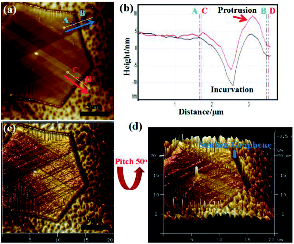 | ||
| Fig. 4 (a) AFM image of the synthesized hexagonal graphene domain. (b) Corresponding line profiles taken along the AB and CD arrows in (a). (c and d) 3D images of (a). | ||
Fig. 5 displays the model of the entire morphological variation of graphene during cooling and etching. As shown in Fig. 5a, C atoms were deposited on the Cu surface to form graphene domains, and the domain edges bent into the Cu substrate at the growth stage.30,31,34 After the growth, when graphene was directly etched at 1050 °C, the etching occurred at the defect positions and the domain edges, which resulted in edge etching, round shape, and etched hexagons inside (Fig. 5b). After the growth, when graphene was cooled down to room temperature, wrinkle structures formed on the graphene surface, and the domain edges sank into the Cu substrate. Fig. 5c illustrates the distinction between etching at 950 and 1000 °C. When graphene was etched at 950 °C, the etching primarily occurred at the wrinkle positions, and the etching at point defects was not evident. Thus, the graphene surface displayed different morphologies of etched trenches (Fig. 5d). When graphene was further reheated to 1000 °C, the expansion and sublimation of the Cu substrate were stronger than those of graphene at 950 °C. Thus, the edge C atoms enfolded by Cu atoms were re-exposed to the hydrogen atmosphere, and the protective effect of Cu atoms weakened, which resulted in edge etching of the graphene domain (Fig. 5e).
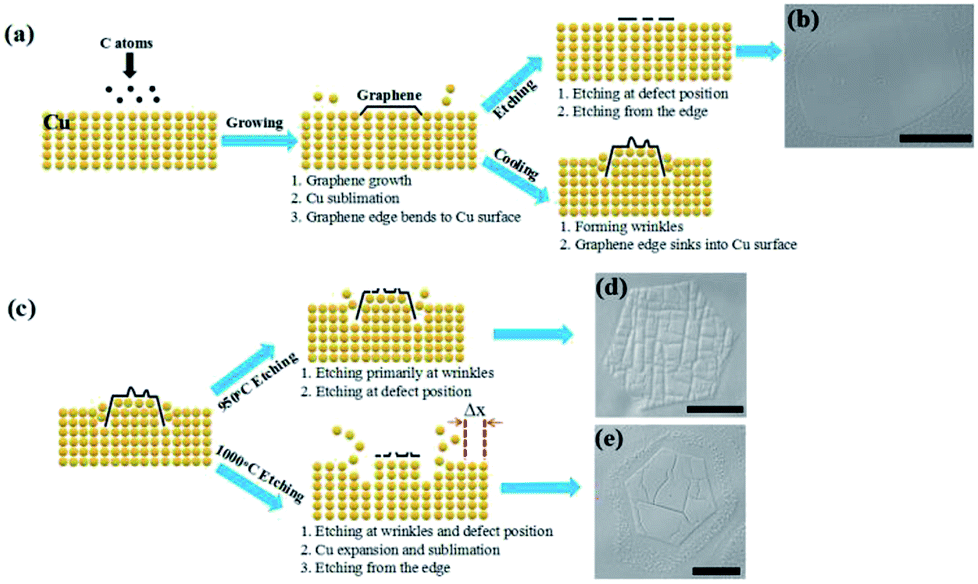 | ||
| Fig. 5 Schematic of the entire morphological variation of graphene during cooling and etching. (a) Process of graphene growth and direct etching; the graphene edge sinks into the Cu substrate during cooling. (b) Optical microscopy image of GED at 1050 °C. (c) Schematic of the distinction between etching at 950 and 1000 °C. (d and e) Optical microscopy images of GECRP at 950 and 1000 °C. The scale bar is 20 μm. | ||
Conclusions
The cooling process induced wrinkle formation on the surface of graphene and resulted in morphology evolution of graphene edges. The influence of cooling-induced edge morphology evolution on H2 etching of graphene edges was studied. The results showed that edge etching was independent of edge morphology or Cu crystal orientation, and it was related to the etching temperature. The visible curvature detected at the graphene edge via AFM indicated the sinking of graphene edge into the Cu surface during CVD cooling. Thus, the edge C atoms were enfolded and protected by the surrounding Cu atoms. As a result, the edge etching of graphene was limited until the etching temperature was increased to 1000 °C. Conclusively, the whole morphological variation of graphene during cooling and etching was illustrated. Our work further elucidated the growth and etching mechanism of CVD graphene on a Cu substrate.Conflicts of interest
There are no conflicts to declare.Acknowledgements
The authors thank Prof. Shilong Lv for assistance in SEM measurements, and thank Prof. Xiaoming Xie for assistance in AFM measurements. The authors thank Yanhui Zhang, Haoran Zhang and Guanghui Yu for useful discussions. This study was supported by the National Natural Science Foundation of China (No. 21503020).Notes and references
- K. S. Novoselov, A. K. Geim, S. V. Morozov, D. Jiang, Y. Zhang and S. V. Dubonos, et al., Electric field effect in atomically thin carbon films, Science, 2004, 306(5696), 666–669 CrossRef CAS.
- A. K. Geim and K. S. Novoselov, The rise of graphene, Nat. Mater., 2007, 6(3), 183–191 CrossRef CAS.
- H. H. Wang, B. Z. Liu, L. Wang, X. D. Chen, Z. L. Chen and Y. Qi, et al., Graphene Glass Inducing Multi-Domain Orientations in Cholesteric Liquid Crystals Devices towards Wide Viewing Angles, ACS Nano, 2018, 12(7), 6443–6451 CrossRef CAS PubMed.
- K. Chen, L. R. Shi, Y. F. Zhang and Z. F. Liu, Scalable chemical-vapour-deposition growth of three-dimensional graphene materials towards energy-related applications, Chem. Soc. Rev., 2018, 47, 3018–3036 RSC.
- R. Raccichini, A. Varzi, S. Passerini and B. Scrosati, The role of graphene for electrochemical energy storage, Nat. Mater., 2015, 14, 271–279 CrossRef CAS.
- K. I. Bolotin, F. Ghahari, M. D. Shulman, H. L. Stormer and P. Kim, Observation of the fractional quantum Hall effect in graphene, Nature, 2009, 462(7270), 196–199 CrossRef CAS.
- A. H. Castro Neto, F. Guines, N. M. R. Peres, K. S. Novoselov and A. K. Geim, The electronic properties of graphene, Rev. Mod. Phys., 2009, 81(1), 109–162 CrossRef CAS.
- J. Y. Sun, Z. L. Chen, L. Yuan, Y. B. Chen, J. Ning and S. W. Liu, et al., Direct Chemical-Vapor-Deposition-Fabricated, Large-Scale Graphene Glass with High Carrier Mobility and Uniformity for Touch Panel Applications, ACS Nano, 2016, 10, 11136–11144 CrossRef CAS.
- H. Wang, G. Z. Wang, P. F. Bao, S. L. Yang, W. Zhu and X. Xie, et al., Controllable Synthesis of Submillimeter Single-Crystal Monolayer Graphene Domains on Copper Foils by Suppressing Nucleation, J. Am. Chem. Soc., 2012, 134(8), 3627–3630 CrossRef CAS.
- K. Lee and J. Ye, Significantly improved thickness uniformity of graphene monolayers grown by chemical vapor deposition by texture and morphology control of the copper foil substrate, Carbon, 2016, 100, 1–6 CrossRef.
- R. Yang, L. C. Zhang, Y. Wang, Z. W. Shi, D. X. Shi and H. J. Gao, et al., An Anisotropic Etching Effect in the Graphene Basal Plane, Adv. Mater., 2010, 22, 4014–4019 CrossRef CAS.
- L. C. Campos, V. R. Manfrinato, J. D. Sanchez-Yamagishi, J. Kong and P. Jarillo-Herrero, Anisotropic Etching and Nanoribbon Formation in Single-Layer Graphene, Nano Lett., 2009, 9, 2600–2604 CrossRef CAS.
- G. J. Cheng, I. Calizo and R. Angela, Hight walker metal-catalyzed etching of graphene governed by metal–carbon interactions: a comparison of Fe and Cu, Carbon, 2015, 81, 678–687 CrossRef CAS.
- H. B. Wang, M. S. Xie, L. Thia, A. Fisher and X. Wang, Strategies on the Design of Nitrogen-Doped Graphene, J. Phys. Chem. Lett., 2014, 5, 119–125 CrossRef CAS.
- X. S. Li, C. W. Magnuson, A. Venugopal, J. H. An, J. W. Suk and B. Y. Han, et al., Graphene Films with Large Domain Size by a Two-Step Chemical Vapor Deposition Process, Nano Lett., 2010, 10(11), 4328–4334 CrossRef CAS.
- X. Sun, L. Lin, L. Z. Sun, J. C. Zhang, D. R. Rui and J. Y. Li, et al., Low-Temperature and Rapid Growth of Large Single-Crystalline Graphene with Ethane, Small, 2017, 1702916, 1–6 Search PubMed.
- I. Vlassiouk, P. Fulvio, H. Meyer, N. Lavrik, S. Dai and P. Datskos, et al., Large scale atmospheric pressure chemical vapor deposition of graphene, Carbon, 2013, 54, 58–67 CrossRef CAS.
- Y. Zhang, L. Y. Zhang and C. W. Zhou, Review of Chemical Vapor Deposition of Graphene and Related Applications, Acc. Chem. Res., 2013, 46(10), 2329–2339 CrossRef CAS.
- B. R. Luo, B. Y. Chen, L. Meng, D. C. Geng, H. T. Liu and J. Xu, et al., Layer-Stacking Growth and Electrical Transport of Hierarchical Graphene Architectures, Adv. Mater., 2014, 26, 3218–3224 CrossRef CAS.
- D. S. Choi, K. S. Kim, H. Kim, Y. Kim, T. Kim and S. H. Rhy, Effect of Cooling Condition on Chemical Vapor Deposition Synthesis of Graphene on Copper Catalyst, ACS Appl. Mater. Interfaces, 2014, 6, 19574–19578 CrossRef CAS.
- B. Wang, Y. H. Zhang, H. R. Zhang, Z. Y. Chen, X. M. Xie and G. H. Yu, et al., Wrinkle-dependent hydrogen etching of chemical vapor deposition-grown graphene domains, Carbon, 2014, 70, 75–80 CrossRef CAS.
- H. R. Zhang, Y. H. Zhang, B. Wang, Z. Y. Chen, Y. Q. Zhang and Y. P. Sui, et al., Stripe distributions of graphene-coated Cu foils and their effects on the reduction of graphene wrinkles, RSC Adv., 2015, 5, 96587–96592 RSC.
- Y. H. Zhang, B. Wang, H. R. Zhang, Z. Y. Chen, Y. Q. Zhang and B. Wang, et al., The distribution of wrinkles and their effects on the oxidation resistance of chemical vapor deposition graphene, Carbon, 2014, 70, 81–86 CrossRef CAS.
- G. H. Han, F. Gunes, J. J. Bae, E. S. Kim, S. J. Chae and H. J. Shin, et al., Influence of Copper Morphology in Forming Nucleation Seeds for Graphene Growth, Nano Lett., 2011, 11, 4144–4148 CrossRef CAS PubMed.
- A. Y. Lu, S. Y. Wei, C. Y. Wu, Y. Hernandez, T. Y. Chen and T. H. Liu, et al., Decoupling of CVD Graphene by Controlled Oxidation of Recrystallized Cu, RSC Adv., 2012, 2, 3008–3013 RSC.
- Y. Zhang, Z. Li, P. Kim, L. Y. Zhang and C. W. Zhou, Anisotropic Hydrogen Etching of Chemical Vapor Deposited Graphene, ACS Nano, 2012, 6, 126–132 CrossRef CAS PubMed.
- T. Ma, W. C. Ren, X. Y. Zhang, Z. B. Liu, Y. Gao and L. C. Yin, et al., Edge-controlled growth and kinetics of single-crystal graphene domains by chemical vapor deposition, Proc. Natl. Acad. Sci. U. S. A., 2013, 110, 20386–20391 CrossRef CAS.
- Y. Zhang, Z. Li, P. Kim, L. Y. Zhang and C. W. Zhou, Anisotropic Hydrogen Etching of Chemical Vapor Deposited Graphene, ACS Nano, 2012, 6(1), 126–132 CrossRef CAS.
- H. R. Zhang, Y. H. Zhang, Y. Q. Zhang, Z. Y. Chen, Y. P. Sui and X. M. Ge, et al., Edge morphology evolution of graphene domains during chemical vapor deposition cooling revealed through hydrogen etching, Nanoscale, 2016, 8, 4145–4150 RSC.
- J. F. Gao, J. J. Zhao and F. Ding, Transition Metal Surface Passivation Induced Graphene Edge Reconstruction, J. Am. Chem. Soc., 2012, 134, 6204–6209 CrossRef CAS PubMed.
- X. Y. Zhang, L. Wang, J. Xin, B. I. Yakobson and F. Ding, Role of hydrogen in graphene chemical vapor deposition growth on a copper surface, J. Am. Chem. Soc., 2014, 136, 3040–3047 CrossRef CAS PubMed.
- D. Yoon, Y. W. Son and H. Cheong, Negative thermal expansion coefficient of graphene measured by Raman spectroscopy, Nano Lett., 2011, 11, 3227–3231 CrossRef CAS PubMed.
- K. V. Zakharchenko, M. I. Katsnelson and A. Fasolino, Finite temperature lattice properties of graphene beyond the quasiharmonic approximation, Phys. Rev. Lett., 2009, 102(046808), 1–4 Search PubMed.
- H. W. Kim, J. Ku, W. Ko, I. Jeon, H. Kwon and S. Ryu, et al., Strong interaction between graphene edge and metal revealed by scanning tunneling microscopy, Carbon, 2014, 78, 190–195 CrossRef CAS.
Footnote |
| † Electronic supplementary information (ESI) available. See DOI: 10.1039/c8ra09265f |
| This journal is © The Royal Society of Chemistry 2019 |