
 Open Access Article
 This Open Access Article is licensed under a Creative Commons Attribution-Non Commercial 3.0 Unported Licence
Formation of a conductive overcoating layer based on hybrid composites to improve the stability of flexible transparent conductive films
Jin-geun Lee,
Wonseok Cho,
Youngno Kim,
Hangyeol Cho,
Hongjoo Lee and
Jung Hyun Kim *
*
Department of Chemical and Biomolecular Engineering, Yonsei University, 50 Yonsei-ro, Seodaemoon-Gu, Seoul, 03722, South Korea. E-mail: Jayhkim@yonsei.ac.kr; Fax: +82 2 312 0305; Tel: +82 2 2123 4693
First published on 4th February 2019
Abstract
A protective layer that can be applied on a flat flexible transparent conductive film was prepared by combining silica sol and organic polymer. (3-Glycidyloxypropyl)trimethoxysilane (GPTMS) was used as a precursor for the silica sol, which hydrolyzed under moisture to form silanol groups and self-condensed to form a sol under acidic conditions. Therefore, the organic polymer used was poly(4-styrenesulfonic acid) (PSSA), which is acidic and water-soluble; thus, the silica precursor can form a sol and can cause chemical condensation with the silica sol under thermal conditions. However, as this protective layer was insulating, there was difficulty in conducting electricity to the lower portion through the upper contact. Therefore, a small amount of conductive polymer, poly(3,4-ethylenedioxythiophene):poly(styrenesulfonate) (PEDOT:PSS), was added to the protective layer to make the overcoating layer itself conductive, thereby enabling electrical conduction to the underlying conductive film. The network structure of the overcoating layer surface could block oxygen and moisture, thus improving chemical stability. Therefore, under high-temperature and high-humidity conditions for 500 h, the sheet resistance increased by 145% before overcoating but increased by 33% after the overcoating layer was formed with appropriate thickness. In addition, the bonding strength of the surface was further improved. Peel-off occurred after applying a pencil having hardness of 5B or more before the overcoating treatment; however, after the overcoating treatment, no damage was caused by a pencil having hardness of 5H or less. Consequently, the overcoated conductive film maintained flexibility and transparency; it also exhibited desirable electrical characteristics, improved chemical stability, and excellent scratch resistance.
Introduction
Electronic materials having wearable characteristics have attracted attention for next-generation applications. Therefore, the demands for transparent and flexible conductive materials are increasing. In particular, conductive polymers are attracting significant attention because they satisfy the requirements of wearable devices owing to their inherent flexibility and desirable optical properties.1–3 Therefore, so far, significant research has been conducted, and conductive polymers have been found to have sufficient conductivity and transparency to be applied to electronic devices.4–6 However, these polymers have very poor stability and their inherent characteristics can easily degrade and deteriorate; hence, they are not actively applied in the industry. These polymers are easily degraded by heat owing to their inherent characteristics7,8 and are easily influenced by oxygen or moisture in the air,9 resulting in the deterioration of their electrical and optical properties.10 In addition, as conductive polymers are easily deformed by the external environment, it is essential to improve their physical and chemical stabilities as well as the desirable electrical and optical properties for their applications in the industry.Therefore, researchers have made various attempts to achieve this goal. Typically, attempts have been made to improve chemical and physical stabilities through the introduction of graphene oxide,11,12 polymers,13–16 inorganic materials,17 and organic silica hybrid complexes.18,19 Each of these methods has achieved the effect of improving stability but inevitably, the electrical characteristics or transparency deteriorate. Overcoating with graphene oxide can produce a highly stable conductive film based on excellent gas-barrier properties and good mechanical properties;20,21 however, owing to the inherent black color of graphene oxide itself, the transmittance in the visible region is very low. A polymer may also be used as a protective layer to improve stability. For example, if polyethylene glycol methyl ether is blended with poly(3,4-ethylenedioxythiophene):poly(styrenesulfonate) (PEDOT:PSS) as a buffer layer,13 water resistance can be improved by lowering the hygroscopicity of the material. However, the effect of improving such chemical stability is not significant, and an improvement in physical stability cannot be expected. Research has also been conducted to deposit inorganic materials. These methods provide increased hardness and desirable mechanical properties; however, as the film itself becomes brittle, it is not sufficiently flexible to be applied to flexible devices. In addition, studies have been carried out to improve stability by overcoating an organic silica hybrid composite synthesized through the sol–gel method.17 Thus, it is possible to produce composite films with desirable mechanical properties and high chemical. In this case, as the conductive layer used was a combination of PEDOT:PSS and silver nanowire, the silver nanowire was placed on the surface of the coated film, due to which electric conduction through the upper contact was possible even after overcoating.22 However, in flat conductive films, when a layer having insulating properties is applied, the electric conduction through the upper contact is limited, and a method for overcoating this has not been reported yet.
Therefore, in this study, an overcoating layer applied to a flat conductive material capable of conducting electricity through the upper contact was formed by combining a silica sol (a polymer having sulfonic groups) and a conductive polymer. Silica precursors hydrolyzed under moisture conditions to form silanol and self-condensed under acidic conditions to form sols through silanol bonds.23 In particular, (3-glycidyloxypropyl)trimethoxysilane (GPTMS) containing an epoxy group was used to form a more compact structure when the formed silica sol bonded with the polymer. These epoxy groups caused the formation of many hydroxy groups on the surface of silica sol through ring-opening reactions under acidic conditions.24–26 Poly(4-styrenesulfonic acid) (PSSA) containing sulfonic acid, which is water-soluble and acidic, was used so that the silica precursor could form a sol. Subsequently, the network structure through the binding of hydroxyl groups and sulfonic acid on the surface of silica sol was induced under thermal conditions.27–29 Since the overcoating layer formed through such bonding exhibited flexibility,30 the conductive composite film to which this layer was applied also maintained flexibility. In addition, a small amount of conducting polymer PEDOT:PSS was added to the network structure layer to induce bonding with the silica sol so that electricity could be conducted to the bottom through the upper contact on a flat film. Thus, the overcoating layer itself was endowed with conductivity. The schematic and chemical structures of this overcoating layer are shown in Fig. 1.
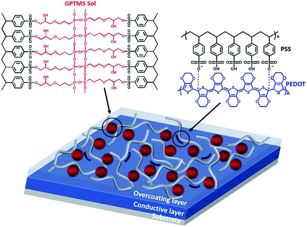 | ||
| Fig. 1 Schematic and chemical structures of the overcoating layer. The overcoating layer forms a network structure through the bond between GPTMS sol and PSSA and contains some PEDOT:PSS. | ||
The conductive film including the formed overcoating layer was flexible and transparent; it also maintained its inherent conductivity and protection from external factors such as oxygen and moisture to improve chemical stability, due to which the electrical characteristics could be maintained for a long time. In addition, the bonding strength improved, and the physical surface hardness increased to provide excellent scratch resistance.
Experimental
Materials
The aqueous dispersion of PEDOT:PSS (PH1000) was purchased from Heraeus Ltd. with a solid content of 1.0–1.3 wt% and a weight ratio of PEDOT:PSS of 1![[thin space (1/6-em)]](https://www.rsc.org/images/entities/char_2009.gif) :2.5. PSSA (Mw ∼75000, 18 wt% in H2O), GPTMS (98%), and dimethyl sulfoxide (DMSO; 98%) were purchased from Sigma-Aldrich Co., Yongin-Si, Gyeonggi-do, Korea.
:2.5. PSSA (Mw ∼75000, 18 wt% in H2O), GPTMS (98%), and dimethyl sulfoxide (DMSO; 98%) were purchased from Sigma-Aldrich Co., Yongin-Si, Gyeonggi-do, Korea.
Preparation of conductive film
First, 5.0 wt% DMSO and 0.1 wt% surfactant were added to the PEDOT:PSS aqueous dispersion, stirred for 10 min, and filtered through a 5.0 μm nylon syringe filter. This dispersion was coated on a PET substrate using an RDS coating bar #7 and dried in a convection oven at 150 °C for 4 min. The thickness of the formed conductive layer was controlled to be approximately 100 nm.Formation of overcoating layer on conductive film
To prepare the solution to be used for the overcoating layer, the PSSA solution was diluted by adding de-ionized water so that the solid content of the PSSA solution became 0.1 wt%. Subsequently, PEDOT:PSS was added to the diluted solution to achieve the desired weight concentration, and GPTMS was added to five times the solid content of PSSA. The hydrolysis and condensation reactions occurred inside the solution, which was stirred at room temperature for 2 h to form a GPTMS sol. This prepared mixed solution was coated on the conductive film using an RDS coating bar and dried in a convection oven at 150 °C for 3 min.Characterization
The atomic force microscopy (AFM) measurements were obtained using the Park Systems apparatus (XE-100) in a non-contact mode to observe the changes in the morphology of the film surface before and after the overcoating. To measure the surface resistance of the conductive film, two instruments were used. A four-point probe resistivity measurement system (NAPSON Corporation, RT-70V/RG-5) was used to measure the surface resistance of 103 Ω sq−1 or less, and a surface resistance meter (SIMCO JAPAN, ST-4) was used to measure the surface resistance of 103 Ω sq−1 or more. A surface profiler (Bruker, DektakXT Stylus Profiler) was used for thickness measurement. The transmittance of the film was measured using UV-vis-NIR spectrophotometry (JASCO Corporation, V-650). Color coordinates were measured using a specialized spectrophotometer (Nippon Denshoku, COH-400). The scratch resistance of the film was measured according to the American Society for Testing and Materials (ASTM) D 3363-92 using a pencil hardness tester (CORE TECH, CT-PC1).Results and discussion
As both the GPTMS sol and the organic polymer PSSA were insulators, the overcoating layer formed by crosslinking the two materials was also an insulator. Therefore, when such an insulating layer was applied on the conductive layer, electrical conduction through the upper contact became difficult because the upper insulating layer hindered the electrical conduction to the underlying conductive layer.Thus, the overcoating layer itself must have conductivity to allow electrical conduction through the top contact even after a long period of time after overcoating. Generally, a substance having electric conductivity between 10−6 and 102 is considered as a semiconductor; a substance having electric conductivity higher than this range is considered as a conductor, and a substance having electric conductivity lower than this range is considered as an insulator.31 Therefore, a solution of PSSA and GPTMS in a weight ratio of 1:5 was prepared; the weight concentration of PEDOT:PSS was adjusted from 0 to 0.04 in the solution, and the coating was performed for measuring conductivity. The conductivity of the overcoating layer was measured, and the results are shown in Fig. 2. Thus, compared with the result for a formulation with PEDOT:PSS weight concentration of 0.01, the conductivity increased drastically in formulations with PEDOT:PSS weight concentration of 0.02 and became similar to that of semiconductors.
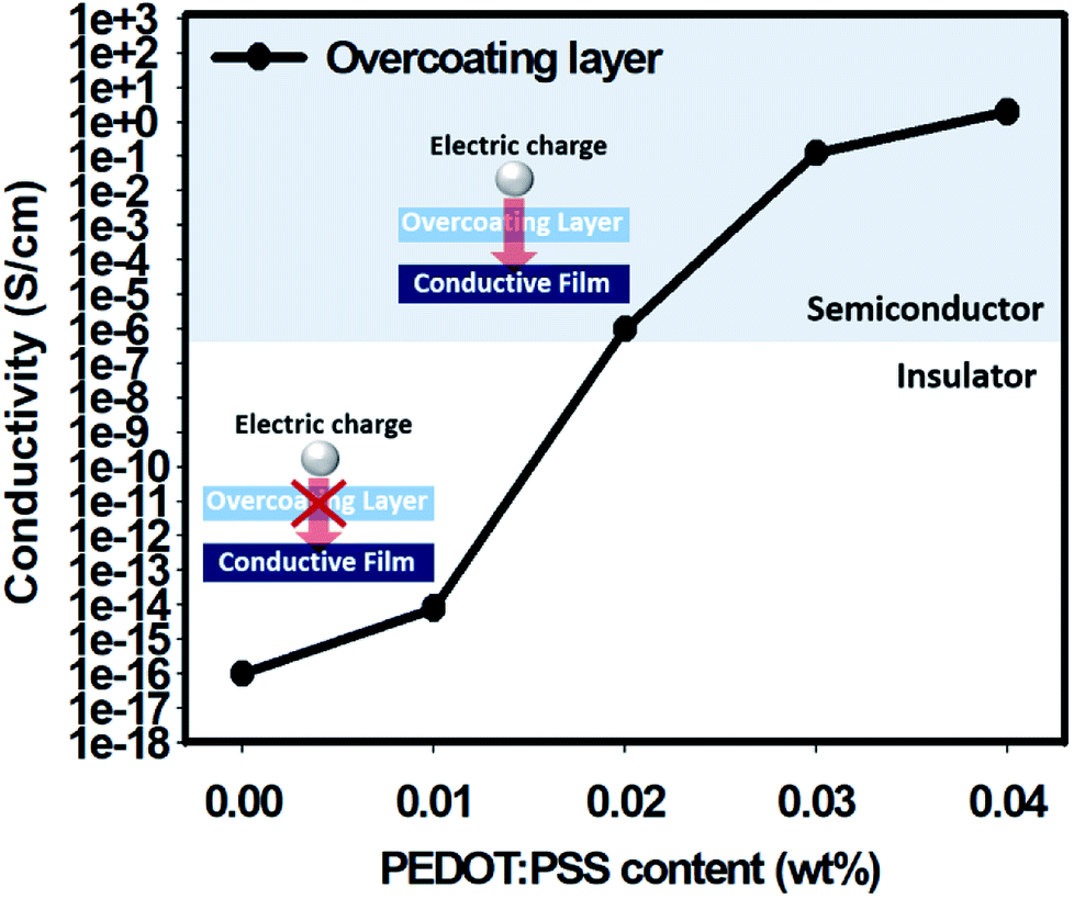 | ||
| Fig. 2 Conductivity according to the PEDOT:PSS content of the overcoating layer. When the content of PEDOT:PSS is less than 0.02 wt%, it is impossible to conduct electricity to the underlying conductive film through the overcoating layer. | ||
Each overcoating layer having different PEDOT:PSS contents was coated onto the conductive film to prepare a composite film, and the conductivity was measured through the upper contact. As a result, the composite film coated with the overcoating layer containing less than 0.02 wt% PEDOT:PSS showed inability to conduct electricity. The composite film coated with the overcoating layer containing 0.02 wt% PEDOT:PSS or more could be measured for conductivity; thus, the electric conduction was smoothly performed.
However, commercialized PEDOT:PSS is very expensive. Therefore, a large amount of PEDOT:PSS cannot be used for industrial applications. In addition, PEDOT:PSS inherently has a very dark blue color. Therefore, it can be expected that the color of the overcoating layer itself can become blue as the ratio of PEDOT:PSS in the overcoating layer increases. This was measured using a colorimeter and expressed as a b* value based on the CIE Lab color space. Here, b* indicates that the larger the negative value, the closer the color to blue. Therefore, as shown in Fig. 3(a), when the PEDOT:PSS content is increased, the color of the overcoating layer becomes dark blue and the b* value becomes high; hence, the transmittance of the overcoated conductive film was lowered and the b* value increased. Fig. 3(b) shows the effect of the increase in the thickness of the overcoating layer on the decrease in the overall transmittance. The b* value also increased as the thickness of the overcoating layer increased. These b* values do not directly affect the transparency, but they can directly cause non-transparency when viewed with the naked eye. Also, it could be seen that the transparency of the overcoated conductive film decreased when the PEDOT:PSS ratio of the overcoating layer was increased. The reason for this result can be explained by the UV-vis-NIR spectra. In Fig. 4, the transmission peak is measured via UV-vis-NIR depending on the thickness of the overcoating layer. As a result of the measurement, it was confirmed that the peak in the visible region near 550 nm gradually decreased as the thickness of the overcoating layer increased, but the difference was not large. Therefore, it could be seen that the transparency of the conductive film was not greatly affected by the overcoating treatment. These spectra also show the doping state of PEDOT present on the film surface before and after overcoating. Generally, the transmission band at approximately 600 nm is related to a neutral chain (NC); the band at approximately 900 nm is ascribed to a radical cation (RC), and the band at 1250 nm and above is attributed to a dication (DC).32 In these spectra, it can be observed that as the thickness of the overcoating layer increases, the transmittance band gradually decreases at around 900 nm, and the transmittance band gradually increases at around 1250 nm. Therefore, it can be seen that after the overcoating treatment, the polaron state PEDOT slightly increased and the bipolaron state PEDOT slightly decreased. This was because the solution used to prepare the overcoating layer contained a small amount of PSSA, but it exhibited a higher pH because most of the solvent is water. This suggested that the state of PEDOT in the overcoating solution changed from bipolaron to polaron.33 Therefore, when the overcoating treatment was performed, PEDOT in the polaron state was added to the film surface; thus, the transmission peak near 900 nm decreased and the remaining GPTMS sol in the overcoating solution bonded with PSSA on the surface of the conductive film. Moreover, PEDOT in the bipolaron state was reduced, and the transmission peak near 1250 nm increased. This indicated that if the thickness of the overcoating layer is excessively increased, the electrical properties of the entire conductive film can degrade.
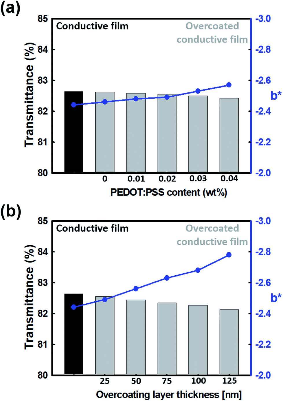 | ||
| Fig. 3 Color coordinates and transmittance according to (a) PEDOT:PSS content of the overcoating layer and (b) the thickness of the overcoating layer. | ||
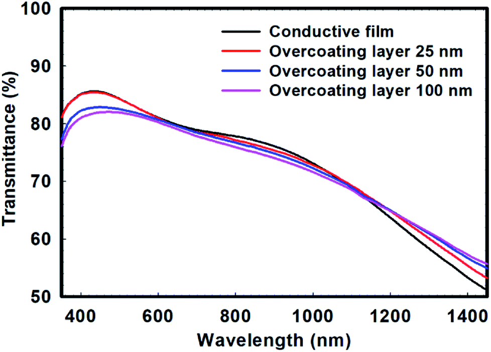 | ||
| Fig. 4 UV-vis-NIR transmission spectra of the PEDOT:PSS conductive film and overcoated conductive films with different thicknesses of the overcoating layer. | ||
PEDOT:PSS has an absorption band in the visible light region but can have transparent characteristics through various controls. This property is important for applications in various fields requiring transparency such as transparent electrodes. Therefore, the optical properties of the conductive films produced using these materials must be well maintained after the overcoating treatment. Therefore, it is necessary to minimize the thickness of the overcoating layer and to adjust the weight concentration of PEDOT:PSS to the minimum possible level of electric conduction.
In Fig. 5, the topographic image is observed through AFM to analyze the shape of the conductive film surface before and after overcoating. It can be seen that the roughness of the surface is reduced after the overcoating treatment as compared to that before the overcoating treatment, which is affected by the thickness of the overcoating layer. In general, the cause of the roughness of PEDOT:PSS is well known as the phase separation of the PEDOT chain and the PSS chain.34 From this viewpoint, the overcoating layer has a small proportion of the PEDOT chain, and the PEDOT ratio is significantly lower than that of PSS because it is mostly composed of PSSA chains and GPTMS sol. Therefore, the phase separation does not appear clearly. Furthermore, as silane was introduced, most of the surface was covered with the GPTMS sol;17 hence, the roughness value of the conductive film before the overcoating treatment was 3.49 nm, and the roughness values after the overcoating treatment were 1.84 nm, 1.72 nm and 1.55 nm depending on the thickness of the overcoating layer. Here, the gradual decrease in roughness with the increase in the thickness of the overcoating layer appeared to be due to the less uniform surface of the underlying conductive film. Therefore, when the overcoating layer having sufficient thickness was formed, roughness value of about 1.55 nm could be regarded as a roughness value of the overcoating layer itself; in other words, after the overcoating treatment, the roughness decreased and the surface became more uniform.
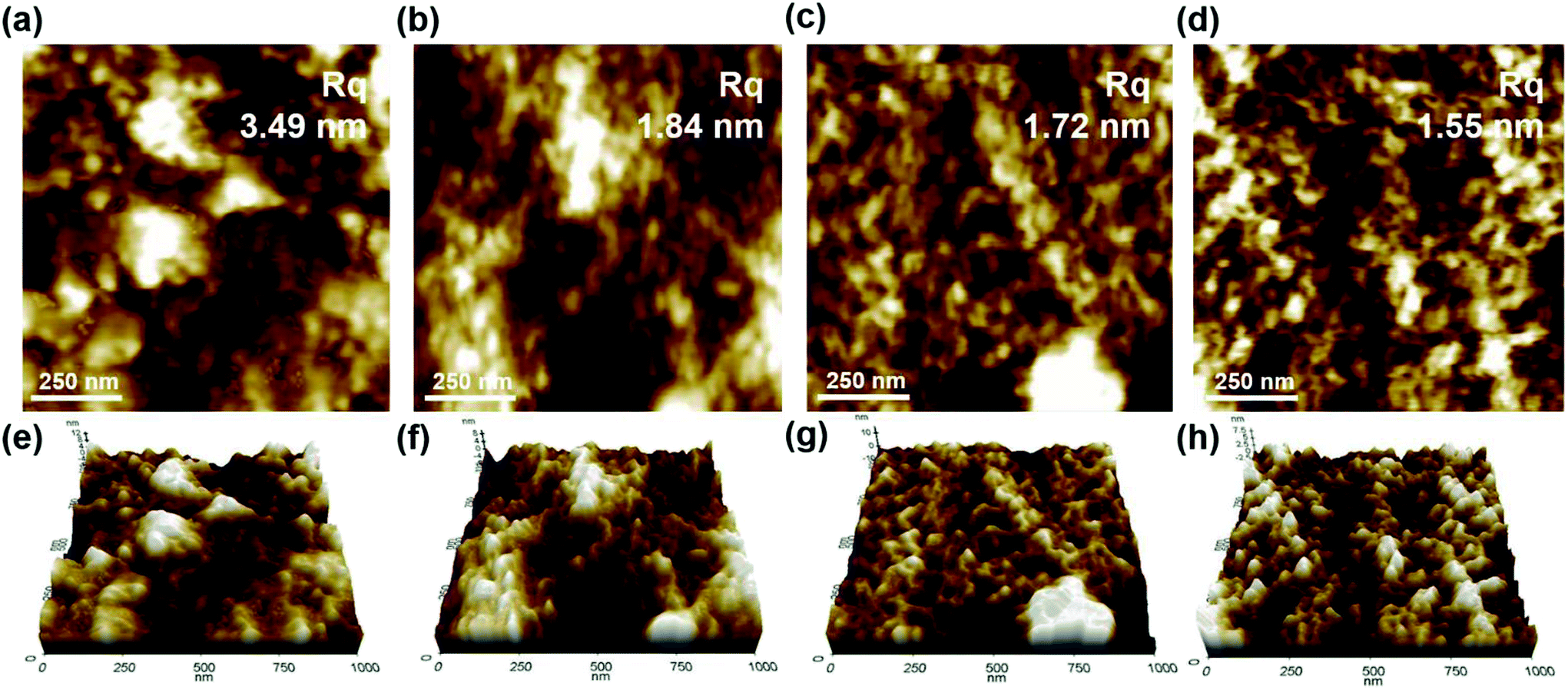 | ||
| Fig. 5 AFM topographical images of the PEDOT:PSS conductive film before and after overcoating treatment. (a and e) Non-overcoating treatment, (b and f) 25 nm, (c and g) 50 nm and (d and h) 100 nm depending on the thickness of the overcoating layer. | ||
As the overcoating layer formed a dense network structure by combining PSSA and GPTMS sol, the hygroscopic sulfonic acid groups on the surface were reduced and were less affected by moisture. In addition, this network structure prevented direct contact between oxygen in the atmosphere and the conductive layer and also improved heat resistance by preventing direct deformation by heat.19 Therefore, through the overcoating process, the sheet resistance could be maintained for a longer time than that in the case without overcoating, due to which the deterioration of the electrical characteristics could be reduced. To verify this, a long-term stability test was conducted under conditions of high temperature and high humidity (85 °C and 85% RH) for 500 h. In Fig. 6, the stability of the overcoated conductive film is compared by adjusting the thickness of the overcoating layer. Fig. 6(a) shows the increase in sheet resistance over time. As a result, the sheet resistance of the conductive film without the overcoating treatment increased sharply by approximately 145% after 500 h; however, after the overcoating treatment, the increase in the sheet resistance was remarkably decreased, and the increase rate of the sheet resistance was only 45% at thickness of 25 nm, 37% at thickness of 50 nm, and 33% at thickness of 100 nm. Thus, it was confirmed that the overcoating treatment improved the chemical stability. Fig. 6(b) shows the degradation of transmittance over time. The transmittance of the conductive film without the overcoating treatment decreased to 80.66% after 500 hours from the initial value of 82.64%. Through the overcoating treatment, when the thickness of the formed overcoating layer was 25 nm, the transmittance decreased from initial 82.55% to 80.88%; the transmittance of the overcoating layer decreased from 82.44% to 80.85% when the thickness of the overcoating layer was 50 nm, and it decreased from 82.27% to 81.04% when the thickness of the overcoating layer was 100 nm. As a result, since the overcoating layer served as a protective layer, the state of the doped PEDOT was maintained for a longer time because the conductive layer was less affected by external factors such as moisture and oxygen. As previously mentioned, as the neutral state of PEDOT increases, the transmittance of visible light decreases.33 Therefore, the transmittance of the conductive layer was maintained for a longer time when the overcoating treatment was performed compared to the result when the overcoating treatment was not performed. This also showed that as the thickness of the overcoating layer increased, the role of the protective layer could be performed in a better manner.
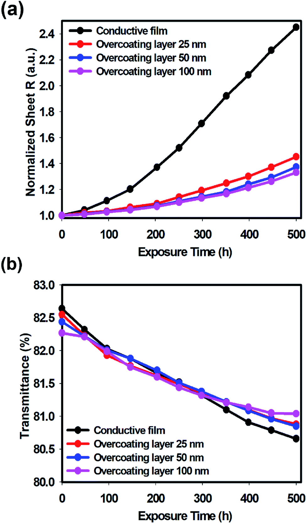 | ||
| Fig. 6 Long-term stability of (a) normalized sheet resistance and (b) transmittance according to the thickness of the overcoating layer of the conductive film under high-temperature and high-humidity (85 °C and 85% RH) conditions. | ||
Organic conductive polymers, such as PEDOT:PSS, generally have soft properties including low scratch resistance and low abrasion resistance.35 Therefore, when a hybrid layer formed by using silica sol was applied to the upper portion, the structure formed through crosslinking exhibited strong bonding force, due to which the hardness of the surface improved and high scratch resistance was obtained.36 Table 1 shows the results of the pencil hardness test according to ASTM Standard D 3363-92.37 Here, the thickness of the overcoating layer was fixed at 25 nm and the measurement was carried out. First, the conductive film before the overcoating was plastic-deformed by the 6B pencil, and the film was completely peeled-off by the 5B pencil with higher strength. However, the conductive film after overcoating did not suffer any damage up to the 5H pencil, and plastic deformation occurred only with the 6H pencil. Therefore, it can be confirmed that the scratch resistance of the conductive film is drastically improved by the overcoating treatment.
| Hardness of pencil | Conductive film | Overcoated conductive film | |
|---|---|---|---|
 |
6H | Peeled-off | Plastic deformation |
| 5H | No damage | ||
| 4H | |||
| 3H | |||
| 2H | |||
| H | |||
| F | |||
| HB | |||
| B | |||
| 2B | |||
| 3B | |||
| 4B | |||
| 5B | |||
| 6B | Plastic deformation | ||
Consequently, the chemical stability and physical hardness of the conductive film increased after the overcoating treatment; thus, it is expected that the conductive film can be stably applied to various devices requiring a conductive film such as a transparent electrode, an organic light-emitting diode, and an organic solar cell.
Conclusions
To improve the stability of the conductive film, a highly transparent and flexible organic/inorganic hybrid protective layer combined with a silica sol and a polymer was developed through a solution-based process. To confirm that this protective layer can be applied to a flat conductive film, this protective layer was overcoated on a conductive film made of PEDOT:PSS to produce a composite film. However, as this overcoating layer exhibited insulating properties, electrical conduction through the upper contact became impossible. Therefore, an appropriate amount of conductive polymer PEDOT:PSS was added to the overcoating layer to endow it with conductivity corresponding to that of a semiconductor. Thus, electric conduction to the lower conductive film through the upper contact became possible after the overcoating treatment. However, since PEDOT:PSS has a blue color in nature, when the content is increased, it may not appear transparent when viewed with the naked eye. Also, when the thickness of the overcoating layer increased, the transparency of the entire film decreased and the electrical properties degraded. Therefore, it is necessary to minimize the amount of PEDOT:PSS added to the overcoating layer and the thickness of the overcoating layer itself at a level at which electrical conduction to the lower conductive film is possible. In addition, the roughness value of the film after the overcoating treatment decreased as compared with that before the treatment, so that it became more flat and was easily applied to various devices; this also improved the stability of the conductive film because it acted as a barrier for moisture absorption and permeation of oxygen. Therefore, in the long-term stability test of 500 hours under conditions of high temperature and high humidity, the sheet resistance of the conductive film without the overcoating treatment increased by more than 145%. The sheet resistance of the conductive film with the thickest protective layer through the overcoating treatment increased only by about 33%. Also, since the doped PEDOT state was maintained, when the transmittance of the conductive film without overcoating decreased by about 2.0%, the transmittance of the conductive film having the thickest overcoating layer was reduced by only 1.2%. Regarding the surface hardness, before the overcoating treatment, plastic deformation occurred with a pencil having hardness of 6B and complete peel-off was observed using a pencil having hardness of 5B or higher. However, after overcoating, plastic deformation occurred only by a pencil with hardness of 6H. Therefore, it can be confirmed that the scratch resistance improved. As a result, we developed a composite conductive film with improved chemical and physical stability while maintaining flexibility, transparency and desirable electrical properties, and it is expected to be used in a wide range of industries requiring such stability. In addition, this overcoating process can be applied to conductive materials other than PEDOT:PSS or advanced optical materials; it is suitable for developing devices based on wearable electronic materials and is expected to have many applications.Conflicts of interest
There are no conflicts to declare.Acknowledgements
This work was supported by the Nano Material Technology Development Program through the National Research Foundation of Korea (NRF) funded by the Ministry of Science, ICT & Future Planning (MSIP, Korea) (NRF-2014M3A7B4050960/2014M3A7B4051745).Notes and references
- M. Y. Teo, N. Kim, S. Kee, B. S. Kim, G. Kim, S. Hong, S. Jung and K. Lee, ACS Appl. Mater. Interfaces, 2017, 9, 819–826 CrossRef CAS PubMed.
- I. del Agua, S. Marina, C. Pitsalidis, D. Mantione, M. Ferro, D. Iandolo, A. Sanchez-Sanchez, G. G. Malliaras, R. M. Owens and D. Mecerreyes, ACS Omega, 2018, 3, 7424–7431 CrossRef CAS PubMed.
- J. E. Lim, S. M. Lee, S. S. Kim, T. W. Kim, H. W. Koo and H. K. Kim, Sci. Rep., 2017, 7, 14685 CrossRef PubMed.
- Y. Xia, K. Sun and J. Ouyang, Adv. Mater., 2012, 24, 2436–2440 CrossRef CAS PubMed.
- N. Kim, S. Kee, S. H. Lee, B. H. Lee, Y. H. Kahng, Y. R. Jo, B. J. Kim and K. Lee, Adv. Mater., 2014, 26, 2268–2272 CrossRef CAS PubMed , 2109.
- S. Kim, B. Sanyoto, W. T. Park, S. Kim, S. Mandal, J. C. Lim, Y. Y. Noh and J. H. Kim, Adv. Mater., 2016, 28, 10149–10154 CrossRef CAS.
- E. Vitoratos, S. Sakkopoulos, E. Dalas, N. Paliatsas, D. Karageorgopoulos, F. Petraki, S. Kennou and S. Choulis, Org. Electron., 2009, 10, 61–66 CrossRef CAS.
- E. Vitoratos, S. Sakkopoulos, N. Paliatsas, K. Emmanouil and S. A. Choulis, Open J. Org. Polym. Mater., 2012, 02, 7–11 CrossRef CAS.
- L. Biessmann, L. P. Kreuzer, T. Widmann, N. Hohn, J. F. Moulin and P. Muller-Buschbaum, ACS Appl. Mater. Interfaces, 2018, 10, 9865–9872 CrossRef CAS PubMed.
- A. M. Nardes, M. Kemerink, M. M. de Kok, E. Vinken, K. Maturova and R. A. J. Janssen, Org. Electron., 2008, 9, 727–734 CrossRef CAS.
- D. Y. Lee, S. I. Na and S. S. Kim, Nanoscale, 2016, 8, 1513–1522 RSC.
- M. Hilal and J. I. Han, Sol. Energy, 2018, 167, 24–34 CrossRef CAS.
- J. J. Lee, S. H. Lee, F. S. Kim, H. H. Choi and J. H. Kim, Org. Electron., 2015, 26, 191–199 CrossRef CAS.
- D. Alemu Mengistie, P.-C. Wang and C.-W. Chu, J. Mater. Chem. A, 2013, 1, 9907–9915 RSC.
- H.-E. Yin, C.-F. Lee and W.-Y. Chiu, Polymer, 2011, 52, 5065–5074 CrossRef CAS.
- W. Cho, J. K. Hong, J. J. Lee, S. Kim, S. Kim, S. Im, D. Yoo and J. H. Kim, RSC Adv., 2016, 6, 63296–63303 RSC.
- W. Cho, S. Im, S. Kim, S. Kim and J. Kim, Polymers, 2016, 8, 189 CrossRef.
- H.-E. Yin, F.-H. Huang and W.-Y. Chiu, J. Mater. Chem., 2012, 22, 14042–14051 RSC.
- S. Kim, A. Cho, S. Kim, W. Cho, M. H. Chung, F. S. Kim and J. H. Kim, RSC Adv., 2016, 6, 19280–19287 RSC.
- I. K. Moon, J. I. Kim, H. Lee, K. Hur, W. C. Kim and H. Lee, Sci. Rep., 2013, 3, 1112 CrossRef.
- Y. Ahn, Y. Jeong and Y. Lee, ACS Appl. Mater. Interfaces, 2012, 4, 6410–6414 CrossRef CAS PubMed.
- S. Kim, S. Y. Kim, M. H. Chung, J. Kim and J. H. Kim, J. Mater. Chem. C, 2015, 3, 5859–5868 RSC.
- L. P. Singh, S. K. Bhattacharyya, R. Kumar, G. Mishra, U. Sharma, G. Singh and S. Ahalawat, Adv. Colloid Interface Sci., 2014, 214, 17–37 CrossRef CAS PubMed.
- D. Işın, N. Kayaman-Apohan and A. Güngör, Prog. Org. Coat., 2009, 65, 477–483 CrossRef.
- P. Innocenzi, C. Figus, T. Kidchob, M. Valentini, B. Alonso and M. Takahashi, Dalton Trans., 2009, 9146–9152 RSC.
- A. J. Worthen, V. Tran, K. A. Cornell, T. M. Truskett and K. P. Johnston, Soft Matter, 2016, 12, 2025–2039 RSC.
- S. Gu, G. He, X. Wu, Y. Guo, H. Liu, L. Peng and G. Xiao, J. Membr. Sci., 2008, 312, 48–58 CrossRef CAS.
- A. Håkansson, S. Han, S. Wang, J. Lu, S. Braun, M. Fahlman, M. Berggren, X. Crispin and S. Fabiano, J. Polym. Sci., Part B: Polym. Phys., 2017, 55, 814–820 CrossRef.
- J. B. P. Andreas, R. Valiokas, B. Liedberg and G. Gauglitz, Biosens. Bioelectron., 2000, 15, 473–481 CrossRef.
- R. Colucci, M. H. Quadros, F. H. Feres, F. B. Maia, F. S. de Vicente, G. C. Faria, L. F. Santos and G. Gozzi, Synth. Met., 2018, 241, 47–53 CrossRef CAS.
- G. Kaur, R. Adhikari, P. Cass, M. Bown and P. Gunatillake, RSC Adv., 2015, 5, 37553–37567 RSC.
- N. Massonnet, A. Carella, O. Jaudouin, P. Rannou, G. Laval, C. Celle and J.-P. Simonato, J. Mater. Chem. C, 2014, 2, 1278–1283 RSC.
- A. Cho, S. Kim, S. Kim, W. Cho, C. Park, F. S. Kim and J. H. Kim, J. Polym. Sci., Part B: Polym. Phys., 2016, 54, 1530–1536 CrossRef CAS.
- W. Kim, S. Kim, S. U. Chai, M. S. Jung, J. K. Nam, J. H. Kim and J. H. Park, Nanoscale, 2017, 9, 12677–12683 RSC.
- I. Imae, S. Takayama, D. Tokita, Y. Ooyama, K. Komaguchi, J. Ohshita, T. Sugioka, K. Kanehira and Y. Harima, Polymer, 2009, 50, 6198–6201 CrossRef CAS.
- I. Imae, Y. Nakamura, K. Komaguchi, Y. Ooyama, J. Ohshita and Y. Harima, Sci. Technol. Adv. Mater., 2012, 13, 045005 CrossRef PubMed.
- The American Society for Testing and Materials (ASTM) D 3363-92 Test Method for Film Hardness by Pencil Test.
| This journal is © The Royal Society of Chemistry 2019 |