
 Open Access Article
 This Open Access Article is licensed under a Creative Commons Attribution-Non Commercial 3.0 Unported Licence
Pd-loaded SnO2 hierarchical nanospheres for a high dynamic range H2S micro sensor†
Yue Suabc,
Peng Chenabc,
Pengjian Wangd,
Jing Gebce,
Shi Hu d,
Yuxin Zhaof,
Gang Xiee,
Wenjie Liang*bcg and
Peng Song*a
d,
Yuxin Zhaof,
Gang Xiee,
Wenjie Liang*bcg and
Peng Song*a
aSchool of Physics, Liaoning University, Shenyang, 110036, P. R. China. E-mail: songpeng@lnu.edu.cn
bBeijing National Center for Condensed Matter Physics, Beijing Key Laboratory for Nanomaterials and Nanodevices, Institute of Physics, Chinese Academy of Sciences, Beijing, 100190, P. R. China. E-mail: wjliang@iphy.ac.cn
cCAS Center of Excellence in Topological Quantum Computation, School of Physical Sciences, University of Chinese Academy of Sciences, Beijing 100190, P. R. China
dDepartment of Chemistry, School of Science, Tianjin Key Laboratory of Molecular Optoelectronic Science, Tianjin University, Tianjin, 300072, P. R. China
eKey Laboratory of Synthetic and Natural Functional Molecule Chemistry of Ministry of Education, College of Chemistry & Materials Science, Northwest University, Xi'an, Shaanxi 710127, P. R. China
fState Key Laboratory of Safety and Control for Chemicals, SINOPEC Research Institute of Safety Engineering, Qingdao, 266071, P. R. China
gSongshan Lake Materials Laboratory, Dongguan, Guangdong 523808, China
First published on 18th February 2019
Abstract
Herein, a high dynamic range H2S micro gas sensor was achieved using hierarchical Pd-loaded SnO2 nanostructures as a sensing material. SnO2 nanospheres were synthesized using a hydrothermal method without any surfactants or templates, followed by Pd nanoparticle decoration via a facile method. A hierarchical nanostructure of Pd-loaded SnO2 was formed, and its sensing abilities were compared with those of pure SnO2 nanosphere-based sensors. The Pd-loaded SnO2 hierarchical nanostructures showed an ultra-sensitive H2S detection ability down to 10 ppb, a high dynamic range (4 orders of magnitude) up to 200 ppm, and a low working temperature (150 °C). Thus, this micro gas sensor based on Pd-loaded SnO2 hierarchical nanostructures has promising applications in universal H2S detection. The fabrication method presented herein is simple, renewable and operable and thus may be extended to synthesize other types of metal oxide-based semiconductor micro sensors for application in various fields.
1. Introduction
In the chemical industry, safety risk because of toxic gases is an important issue; therefore, the demand for the detection and monitoring of toxic gases is very high. Among dangerous gases, hydrogen sulphide (H2S) is a common toxic, colorless gas pollutant. Although the occupational exposure limit for H2S is 10 ppm for 8 h exposure, the acceptable ambient concentration of H2S (recommended by the Scientific Advisory Board on Toxic Air Pollutants USA) is under 20–100 ppb.1 Thus, the detection of H2S at the ppb level is crucial. Moreover, H2S is a corrosive gas, and at high concentrations, H2S can damage the sensor. Thus, the achievement of a large dynamic range sensor is difficult.Semiconductor sensors are widely studied and used, which mainly consist of metal-oxide semiconductors (MOSs).2–4 Compared with other types of sensors, they have a fast response, wide gas response concentration range, low cost, easy operation and portability. Common sensitive metal-oxide semiconductors are SnO2,5–7 ZnO,8,9 Fe2O3,10,11 WO3 (ref. 12 and 13) and In2O3.14,15 When exposed to the target gas, these oxides respond with resistive changes and are suitable for sensing. SnO2, ZnO and Fe2O3 have a good gas sensing property for reducing gases and combustible gases, whereas WO3 and In2O3 show good sensing property for oxidizing gases. Tin oxide (SnO2) is one of the typical n-type metal-oxide semiconductors with a wide band gap (Eg = 3.6 eV at 300 K). Due to their large surface-to-volume ratios, nanostructured SnO2, including nanoparticles, nanowires and thin films,16–19 have been developed to achieve enhanced sensing capabilities.20 Using a nanostructure with a large surface-to-volume ratio, the SnO2 gas sensors showed improved resistive responses when exposed to target gases.20–22 Further improvement, such as in terms of the detection range and selectivity, of the gas sensing performance was achieved via surface loading of noble metals,23–27 for example Au,28,29 Ag,20,30,31 Pd32,33 and Pt.34,35 Compared with other metals, palladium (Pd) has a low binding energy, and the low barriers for hydrogen dissociation and oxygen adsorption reduce the activation energy; thus, it can affect the conductivity and gas response of the sensitive membrane of the sensor.
In this study, we developed an ultra-sensitive H2S micro gas sensor with 2% Pd-loaded SnO2 hierarchical nanostructures based on pure SnO2 nanospheres, fabricated by hydrothermal and micro-nano processing technology. The micro gas sensor used interdigital Cr/Au electrodes (300 μm × 300 μm) coated with the Pd-loaded SnO2 nanostructures. Micro gas sensors have low cost, low energy consumption and ability of sensor array integration. The gas sensing ability was tested in ambient air using a precise electrical meter to measure the gas response capabilities. For comparison, a pure SnO2 nanosphere sensing film was deposited on a micro sensing chip. We demonstrated that Pd-loaded SnO2 had a hierarchical nanostructure as compared to the pure SnO2 nanospheres and showed a high gas response (5 ppm/27.6), an ultra-sensitive detection limit, a wide detection range (10 ppb to 200 ppm) and a low operating temperature (down to 150 °C).
2. Experimental
2.1 Preparation of the Pd-loaded SnO2 nanospheres
SnCl2·2H2O (0.45 g), oxalic acid (0.8 g), hydrazine hydrate (5.856 g), and hydrochloric acid (0.08 mL) were dissolved in deionized water (37.8 mL) to form a clear and colorless mixture solution. After being stirred for 30 min, the solution was put in a 40 mL Teflon liner followed by heating to 180 °C for 24 h. The resulting product was washed with double distilled water and further dried at 60 °C in air to obtain the SnO2 powder. Subsequently, the SnO2 powder was heated to 600 °C at the ramping rate of 5 °C min−1 in a tube furnace under flowing air, and the temperature was maintained at 600 °C for 2 h.The Pd-loaded SnO2 nanospheres were synthesized by solvent evaporation as follows: 100 mg SnO2 powder was suspended in 1 mL ethanol under stirring. Moreover, 1 mL PdCl2 (2 wt%, where wt% is the mean of weight percent) was added and dissolved in the obtained solution. After stirring for 10 min, the solution was transferred to a centrifuge tube to evaporate the solvent at 80 °C in a water bath until the solvent was completely removed. The final products were obtained and subsequently annealed at 500 °C for 1 h at the heating rate of 5 °C min−1 in air.
All reagents and materials used in the present experiment were of analytical grade and applied without further purification. Double-distilled water was used throughout all the experiments.
2.2 Material characterization
The crystal structure of our samples was characterized using Bruker D8 XRD with Cu-Kα radiation (λ = 1.5419 Å) at room temperature. The morphology of the final products was investigated using scanning electron microscopy (SEM, Carl Zeiss, ZEISS SIGMA). Transmission electron microscopy (TEM) and high-resolution transmission electron microscopy (HRTEM) analysis were performed using JEOL-2010 at the accelerating voltage of 200 kV.2.3 Fabrication of micro gas sensors and measurement of the gas-sensing performance
Our micro gas sensors were composed of 300 μm sized interdigitated gold electrodes covered with Pd-loaded SnO2 nanospheres as well as pure SnO2 nanospheres for comparison. The interdigitated electrodes were fabricated on silicon dioxide (SiO2) with a thickness of about 300 nm by photolithography, followed by deposition with Cr/Au (5/100 nm) by thermal evaporation. The vacuum value during evaporation was under 5 × 10⁻⁷ mbar. The deposition rate of Cr and Au was 0.1 Å s−1 and 1 Å s−1, respectively. The interdigitated electrode spacing was 30 μm, and the electrode width was 15 μm. Finally, the sensor chips were placed in acetone for 5–6 h, and the unwanted metal was removed.The as-prepared Pd-loaded SnO2 nanospheres were dispersed in terpineol at the mass ratio of 8![[thin space (1/6-em)]](https://www.rsc.org/images/entities/char_2009.gif) :5 to form a paste. After grinding for 10 min, the obtained paste was transferred to the SiO2/Si substrate with an interdigitated electrode, followed by drying at 40 °C for 12 h to remove the solvent. The obtained sensor film was annealed at 300 °C for 20 min before measurement to further improve the response and stability. Finally, the chip was fixed in a chip carrier with silver paste and wire bonded using a Si/Al wire.
:5 to form a paste. After grinding for 10 min, the obtained paste was transferred to the SiO2/Si substrate with an interdigitated electrode, followed by drying at 40 °C for 12 h to remove the solvent. The obtained sensor film was annealed at 300 °C for 20 min before measurement to further improve the response and stability. Finally, the chip was fixed in a chip carrier with silver paste and wire bonded using a Si/Al wire.
The gas-sensing measurement was performed using H2S with concentration ranging from 10 ppb to 200 ppm at the operation temperature of 150–350 °C. After the micro sensor was heated to the target temperature and its resistance was stabilized, a calculated volume of the gas was injected into the test chamber (2 liters) using a micro-injector. As is known, relative humidity can play an important role in the gas sensing performance.36,37 Therefore, we carefully monitored the relative humidity in our test environment. All measurements in this study were conducted at about 30 ± 5% relative humidity and at a room temperature of 25 ± 5 °C. The gas response was calculated based on the equation S = (Rair − Rgas)/Rgas, where Rair is the resistance of the sensor in air and Rgas is the resistance of the sensor exposed to the target gas environment.
3. Results and discussion
3.1 Structure and morphology
The morphology and structure of the pure SnO2 nanosphere particles and Pd-loaded SnO2 nanosphere particles were characterized via SEM, TEM and XRD. Fig. 1 shows the SEM images of both samples. The pure SnO2 nanospheres have a smooth surface, and their diameter is about 1 μm (Fig. 1a). On the other hand, the Pd-modified SnO2 nanospheres show a rough surface and fine nanostructures. Their surface area increased after Pd loading; however, the overall size remained unchanged (Fig. 1b and c). A layered structure could be seen, and the nanosheets protruded out of the sphere. An increase in the surface area results in more active sites for target gas sensing, and more contact sites via the nanosheets between adjacent nanospheres will enhance the sensitivities. Elementary mapping by EDX (Fig. 1d) shows that the distribution and formation of O, Sn, and Pd elements are uniform on the nanosphere surface. This confirms that Pd ions have been successfully loaded on the SnO2 surface.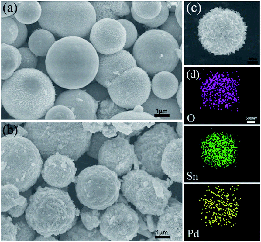 | ||
| Fig. 1 SEM images of the (a) pure SnO2 nanosphere structures, (b) Pd-loaded SnO2 nanosphere structures, and (c) single Pd-loaded SnO2 nanosphere structures, and (d) SEM-EDX elemental mapping images of (c) single Pd-loaded SnO2 nanosphere structure. | ||
XRD analysis was used to determine the phase structures of the as-prepared pure SnO2 and Pd-loaded SnO2 powders. The XRD pattern of both the SnO2 and Pd-loaded SnO2 nanosphere structures reflect the monoclinic structure of SnO2 [JCPDS card, no. 41-1445, space group: P42/mnm (136)], which was confirmed by HRTEM in Fig. 2. In these two spectra, there are no obvious characteristic peaks of Pd species mainly due to the low amount of Pd and extremely small size of the well-dispersed Pd NPs on the surface surrounded by the crystalline SnO2 nanospheres. Moreover, no diffraction peaks of the palladium metal and other impurity phase were observed.
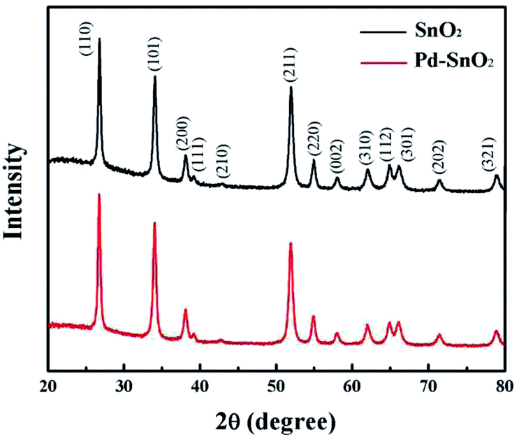 | ||
| Fig. 2 XRD patterns of the pure SnO2 nanosphere structures (top) and the Pd-loaded SnO2 nanosphere structures (bottom). | ||
The influence of Pd loading on the microstructure of the SnO2 nanoparticles was most obvious in the HRTEM image. Fig. 3a–c show the HRTEM images of the Pd-loaded nanospheres at different scales. The SnO2 nanospheres with diameter in the range of 1 μm (Fig. 3a) were surrounded by thin layers of nanosheets (Fig. 3b). Moreover, the Pd nanoparticle loadings can be clearly seen (Fig. 3c), revealing a high crystallinity of SnO2 and Pd particles. The interplanar spacing of d = 0.334 nm and d = 0.264 nm corresponded to the {110} and {101} crystal orientation of SnO2 [JCPDS card, no. 41-1445], respectively, and d = 0.224 nm matched the {111} orientation of Pd [JCPDS card, no. 87-0639]. The loaded Pd nanoparticles have been previously proven to enhance the gas response and selectivity.25,38–40 Herein, based on previous studies, 2% loading was chosen as the optimum doping percentage.40–49
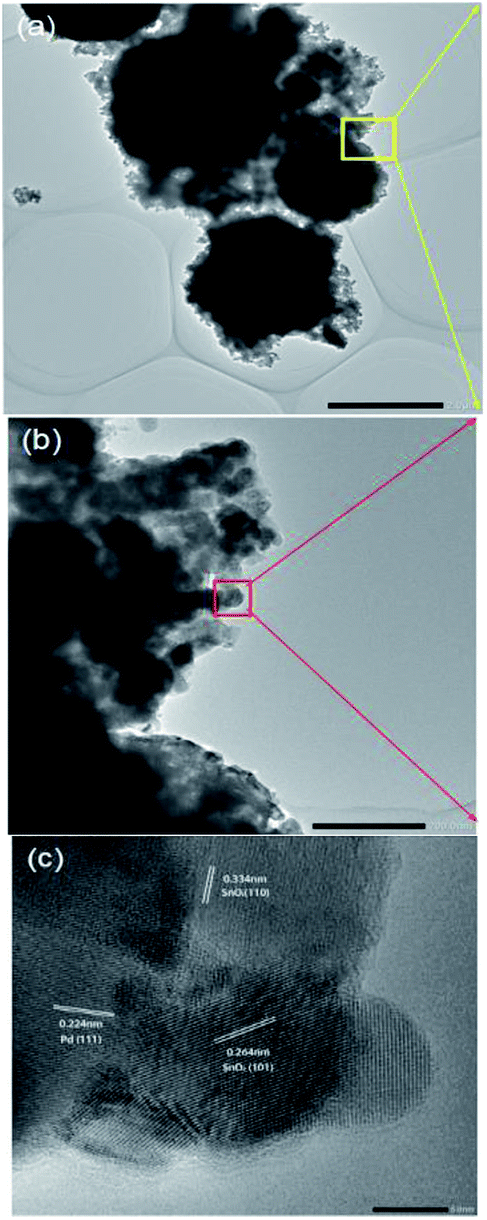 | ||
| Fig. 3 HRTEM images of the Pd-loaded SnO2 nanosphere structure at different scales. Scale bars are 2 μm in (a), 200 nm in (b), and 5 nm in (c). | ||
Based on the abovementioned analysis, the Pd-loaded SnO2 nanospheres have hierarchical structures, combining nanospheres, nanosheets and nanoparticles, ranging from 1 μm to 100 nm and 5 nm. Hierarchical structures are ideal for the purpose of gas sensing, which provide high surface area and a stable porous structure.7
3.2 Gas sensing properties of the Pd-loaded SnO2 nanosphere microsensors
When SnO2 was exposed to a reducing gas, such as hydrogen sulfide, physical and chemical absorption occurred, which changed the electronic exchange in materials and the conductivity of SnO2. When exposed to H2S gas at different concentrations, our micro gas sensors showed a wide response range from 10 ppb to 200 ppm. The typical full range H2S gas measurement of our micro sensors is illustrated in Fig. 4. Response at 10 ppb of H2S was 2% with a signal-to-noise ratio of about 4, well above the requirement for signal recognition. The gas response increased with an increase in the H2S concentration (Fig. 4b red dot) to up to 50 ppm; moreover, the response at 50 ppm was 42.8. Above 50 ppm concentration, the response of the sensors to gas was saturated, and it decreased when the sensors were exposed to a higher concentration of gas due to the poison effect.50–53 In our corrosion gas environment, poisoning effect is the strong chemisorption of H2S on the catalytic sites; this accordingly blocks the sites for catalytic reaction, and thus, the sensors lose their ability for sensing. Our micro sensor showed good gas responses up to the highest concentration of 200 ppm tested herein. Moreover, we examined the micro gas sensors with pure SnO2 nanospheres as the sensing materials. The result is shown in Fig. 4b (black dot).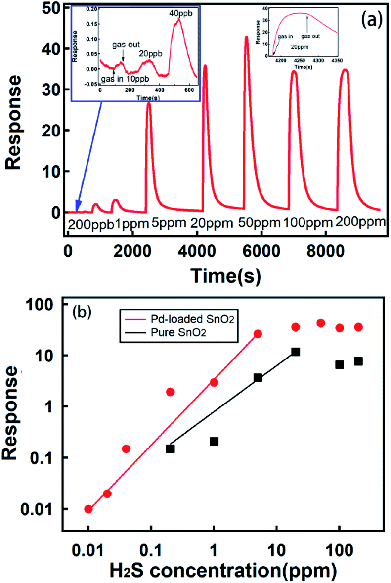 | ||
| Fig. 4 (a) The response of the Pd-loaded SnO2 nanosphere sensor towards the detection of H2S gas at various concentrations from 10 ppb to 200 ppm at an optimal operation temperature of 200 °C. The inset shows the response of the Pd-loaded SnO2 nanosphere sensor towards the detection of H2S gas with concentrations from 10 ppb to 40 ppb and 20 ppm at an operation temperature of 200 °C. (b) The response logarithm curves of the Pd-loaded and pure SnO2 nanosphere sensors to H2S gas at various concentrations at an operation temperature of 200 °C. | ||
These sensors show a credible gas response up to 200 ppb, and their observed response to gas exposure is 3 to 14 times lower than that for Pd-loaded samples in the test range. Our concentration-dependent data can be seen to follow a power law relation,54 which is used to describe the sensing characteristics of SnO2 sensors and can be written as follows:
| S = kCα |
Based on these analyses, it can be concluded that a micro gas sensor based on Pd-loaded SnO2 nanospheres has a credible gas detection ability down to 10 ppb (with a good signal-to-noise ratio of 4) and 4 orders of magnitude concentration detection ranges (up to 200 ppm). Its gas response and detection limit was much better than that of pure SnO2 nanosphere sensor. Response of the pure SnO2 nanosphere obviously increased after it was loaded with Pd; this could be attributed to the formation of hierarchical structures. Moreover, the Pd nanoparticle loading increased the rate of oxygen dissolution, and the Pd nanoparticles played the role of a catalyst. We also observed that a high concentration of grain boundaries (Fig. 3c) would play an important role in enhanced gas sensing.7
Indeed, it is hard to obtain a gas sensor with both an ultra-sensitive gas detection ability and a large detection range. To the best of our knowledge, four orders of magnitude dynamic ranges for H2S sensing are unprecedented. We attribute the combination of these two merits in one micro gas sensor to the fact that we created hierarchical structures on the SnO2 nanosphere surfaces. Obviously, nanosheets of up to 10 nm (Fig. 3c) contacting each other (Fig. 3b) were responsible for an ultra-sensitive response. The nanometer-sized sensing materials have shown superior detecting ability down to sub-ppb level in the past.55–59 Moreover, large nanospheres of up to 2 μm size possibly accounted for a high concentration (100 ppm) detection, which was the case for our pure SnO2 nanosphere sensors (Fig. 4b).
The gas sensing ability depends on the physical and chemical absorption properties of a gas, which strongly depend on temperature. We investigated the optimal working temperature of the Pd-loaded and pure SnO2 nanosphere gas sensor. The experimental conditions, as shown in Fig. 5, are as follows: environmental temperature of 25 °C ± 5 °C and humidity around 30% ± 5% with 1 ppm as the test concentration of H2S. For comparison, the pure SnO2 nanosphere and Pd-loaded SnO2 nanosphere micro gas sensors were simultaneously tested in 1 ppm H2S at a series of temperatures. We changed the test temperature from 150 to 350 °C with a 50 °C integral (Fig. 5). The Pd-loaded SnO2 nanosphere micro gas sensor and pure SnO2 nanosphere micro gas sensor were fabricated using the same method listed. Compared with the pure SnO2 nanosphere sensors, the Pd-loaded SnO2 nanosphere sensors showed a large temperature dependence. They provided highest responses at a temperature of 150 °C.
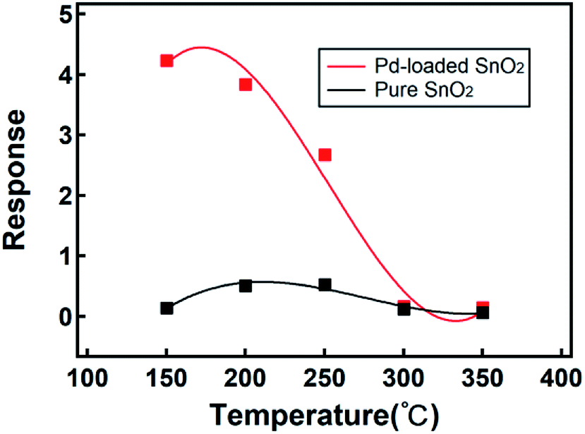 | ||
| Fig. 5 The response of Pd-loaded (red) and pure (black) SnO2 nanosphere sensors to 1 ppm H2S at different working temperatures. | ||
For the pure SnO2 samples, the highest responses appeared at 200 °C (Fig. 5). A lower working temperature indicated a lower power consumption rate, which was crucial for micro gas sensors in portable devices. Moreover, a lower working temperature indicated a more stable structure and repeatability of sensors. The response difference between the Pd-loaded samples and the pure sample at 150 °C is 30. As the working temperature increased, the response difference between the two types of sensors decreased, and finally, above 300 °C, their gas sensitivities were at the same level. If the response enhancement is lost above 300 °C, small features in the hierarchical Pd-loaded SnO2 nanostructures and their advantages at a high temperature are lost; although the exact mechanism requires further investigation, some studies have indicated that a higher carrier concentration in nanosheets at a high temperature can be a reason for the decrease in gas response.60
Selectivity is an important index for the gas sensing properties. Hence, the sensor should have a high selectivity for its application. Fig. 6a shows the response of the Pd-loaded and pure SnO2 to seven gases, i.e., CO, NH3, CH4, toluene, ethanol, and isopropanol at a concentration of 5000 ppm and H2S at 20 ppm at 200 °C. Note that the sensor exhibits highest response to H2S and lower responses to other gases. After Pd loading on the SnO2 surface, the response to the gases increased more than ten times of that expected for NH3 and CH4. In particular, the sensor was insensitive to CH4. Moreover, the experimental results indicate that the Pd-loaded SnO2 nanosphere sensor shows a high selectively for the detection of H2S gas and can distinguish a small amount of H2S among 5000 ppm of the interfering gases; this makes the proposed sensor promising for monitoring the extremely dilute leakage of H2S gas. The response and recovery times are two significant indices in assessing the gas sensing performance of sensors, which are also related to the detection speed of the sensor. The response and recovery time is defined as the time to reach 90% of the maximum sensing response when the target gas is injected into the test chamber. Similarly, the time for the maximum sensing response decreased to 10% upon air purging.76 Fig. 6b and c show the response and recovery times of the sensor based on the Pd-loaded SnO2 nanosphere thin film upon exposure to 20 ppm H2S and 5000 ppm of other interfering gases at the working temperature of about 200 °C. It is obvious that for most test gases (expect toluene), the sensor recovery time is slow as compared to the response time. A long recovery time at a low working temperature can be due to the sluggish serial reactions referring to the adsorption, dissociation, and ionization of oxygen on the surface.61 After Pd loading, the response time was reduced from 44–371 s to 15–97 s and the recovery time was reduced from 130–370 s to 80–300 s for the interfering gases at 5000 ppm and H2S at 200 °C. Therefore, the increase in the response speed caused by Pd loading can be explained by the promotion of the oxidation reaction between H2S and the negatively charged surface oxygen because of the Pd catalyst.77 In general, the Pd-loaded SnO2 nanosphere gas sensors show wonderful selectivity and response and recovery speed for the interfering and target gases; thus, the proposed sensor is helpful in detecting the extremely attenuate leakage of H2S gas.
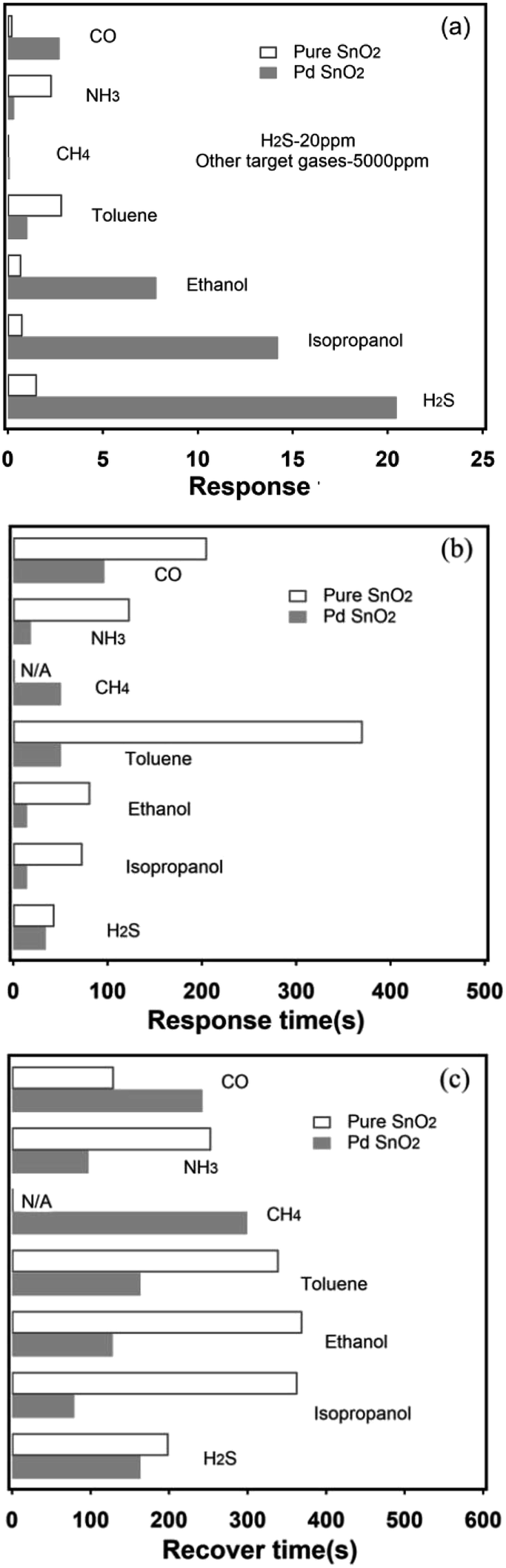 | ||
| Fig. 6 (a) The sensitivity of Pd-loaded (gray) and pure (white) SnO2 to interfering gases in a concentration of 5000 ppm and 20 ppm to H2S gases at working temperature of 200 °C. (b) Response and (c) recover times of Pd-loaded (gray) and pure (white) SnO2 upon different gases in a concentration of 5000 ppm and 20 ppm to H2S gases at working temperature of 200 °C. | ||
Table 1 presents the comparison of the sensor materials and the concentration range for the H2S sensors reported earlier and in this study. It can be clearly seen that the Pd-loaded SnO2 nanosphere structured materials show a low detectable concentration and a high dynamic range for H2S at an optimal working temperature. Compared with the case of other H2S sensors reported to date, a low detectable concentration and high dynamic range at a low operation temperature have been accomplished in this study.
| Sensor materials | Concentration range | Dynamic range | Temperature | References |
|---|---|---|---|---|
| a Please see the ESI. | ||||
| SnO2/ZnO heteronanostructures | 10 ppb | 103 | 100 °C | 9 |
| CuxO-doped SnO2 film | 500 ppb | 101 | Room temperature | 61 |
| CuO-doped SnO2 | 100 | 101 | 200 °C | 62 |
| SnO2 | 1 ppm | 101 | 200 °C | 63 |
| Pt-WO3 nanotube | 150 ppb | 101 | 450 °C | 64 |
| ZnO film | 1 ppm | 100 | 450 °C | 65 |
| ZnFe2O4 nanofiber | 100 ppb | 101 | 350 °C | 66 |
| Carbon nanotube | 5 ppb | 103 | Room temperature | 67 |
| NiO nanosheet | 25 ppm | 102 | 350 °C | 68 |
| Ag–SnO2 film | 1 ppm | 101 | 200 °C | 69 |
| Zn2SnO4 lamellar micro-spheres | 50 ppb | 102 | 170 °C | 70 |
| Au nanostars/ZnO mesocrystal | 5 ppb | 103 | 100 °C | 71 |
| ZnO nanowires | 50 ppb | 100 | 150 °C | 72 |
| K2W4O13 nanowires | 300 ppb | 102 | 300 °C | 73 |
| Sb-doped SnO2 nanoribbon | 100 ppb | 103 | 25 °C | 74 |
| Mo-doped ZnO nanowires | 200 ppb | 101 | 300 °C | 75 |
| Pd-loaded SnO2 | 10 ppb | 104 | 150 °C | This worka |
To test the repeatability and reproducibility, we investigated more than 20 Pd-loaded SnO2 sensors for a week. The results of the 9 sensors are exhibited in the ESI.† The performance was similar for different devices. Fig. 3 of the ESI† shows that a response to 1 ppm of H2S for different devices varies between 3 and 15. A similar response is noticed for concentration (please refer to Fig. 1 of the ESI†) and aging also (please refer to Fig. 3 of the ESI†); however, stability is still not ideal. For ultra-sensitive micro sensors, many factors would contribute to damage the repeatability. We are working on illustrating some of the important factors. The number of active sites and the point of contact play a decisive role, and the details will be described in the next study.
4. Conclusions
In summary, micro H2S gas sensors based on Pd-loaded SnO2 hierarchical nanospheres were achieved using a simple hydro-thermal method. Structural analysis shows a hierarchical structure with nanospheres and nanosheets, loaded with Pd nanoparticles. These micro sensors are proven to have an ultra-sensitive ppb level (10 ppb) H2S detection ability and wide detection range (up to hundreds of ppm) at the same time. The Pd-loaded SnO2 nanosphere micro-chips work best at low temperatures (150 °C); this is crucial for low-power consumption applications. Our Pd-loaded SnO2 nanosphere micro gas sensors are cost-effective, easy to make, simple to operate and ultra-sensitive for the detection of H2S with a wide detection range. The fabrication method presented herein is simple, renewable and operable and thus may be extended to synthesize other types of metal oxide-based semiconductor micro sensors for applications in various fields.Conflicts of interest
The authors declare no competing financial interests.Acknowledgements
This research was supported by the National Basic Research Program of China (2014CB920904), the National Natural Science Foundation of China (NSFC, Grant No. 21601133, 61701543), the Strategic Priority Research Program of Chinese Academy of Sciences (Grant No. XDB30000000), and the Strategic Priority Research Program of Chinese Academy of Sciences (Grant No. XDB07030100), Sinopec Innovation Scheme (A-381).Notes and references
- M. Kaur, N. Jain, K. Sharma, S. Bhattacharya, M. Roy, A. K. Tyagi, S. K. Gupta and J. V. Yakhmi, Sens. Actuators, B, 2008, 133, 456–461 CrossRef CAS.
- M. Righettoni, A. Amann and S. E. Pratsinis, Mater. Today, 2015, 18, 163–171 CrossRef CAS.
- D. Yang, M. K. Fuadi, K. Kang, D. Kim, Z. Li and I. Park, ACS Appl. Mater. Interfaces, 2015, 7, 10152–10161 CrossRef CAS PubMed.
- X.-J. Huang and Y.-K. Choi, Sens. Actuators, B, 2007, 122, 659–671 CrossRef CAS.
- I. T. Weber, A. Valentini, L. F. D. Probst, E. Longo and E. R. Leite, Sens. Actuators, B, 2004, 97, 31–38 CrossRef CAS.
- J. Gong, Q. Chen, M.-R. Lian, N.-C. Liu, R. G. Stevenson and F. Adami, Sens. Actuators, B, 2006, 114, 32–39 CrossRef CAS.
- Y. X. Li, Z. Guo, Y. Su, X. B. Jin, X. H. Tang, J. R. Huang, X. J. Huang, M. Q. Li and J. H. Liu, ACS Sens., 2017, 2, 102–110 CrossRef CAS PubMed.
- M. Chen, Z. Wang, D. Han, F. Gu and G. Guo, J. Phys. Chem. C, 2011, 115, 12763–12773 CrossRef CAS.
- D. Fu, C. Zhu, X. Zhang, C. Li and Y. Chen, J. Mater. Chem. A, 2016, 4, 1390–1398 RSC.
- Y. Cheng, Y. He, S. Li, Y. Wang, Y. Zhao, Y. Li, H. Li and L. Liu, J. Mater. Sci.: Mater. Electron., 2018, 29, 11178–11186 CrossRef CAS.
- Y. Wang, Y. Wang, J. Cao, F. Kong, H. Xia, J. Zhang, B. Zhu, S. Wang and S. Wu, Sens. Actuators, B, 2008, 131, 183–189 CrossRef CAS.
- N. M. Vuong, D. Kim and H. Kim, Sci. Rep., 2015, 5, 11040 CrossRef PubMed.
- Q.-q. Jia, H.-m. Ji, P. Gao, X. Bai and Z.-g. Jin, J. Mater. Sci.: Mater. Electron., 2015, 26, 5792–5802 CrossRef CAS.
- J. Wang, Z. Zheng, D. An, X. Tong and Q. Zhou, Mater. Sci. Semicond. Process., 2018, 83, 139–143 CrossRef CAS.
- D. Han, L. Zhai, F. Gu and Z. Wang, Sens. Actuators, B, 2018, 262, 655–663 CrossRef CAS.
- K.-W. Kim, P.-S. Cho, S.-J. Kim, J.-H. Lee, C.-Y. Kang, J.-S. Kim and S.-J. Yoon, Sens. Actuators, B, 2007, 123, 318–324 CrossRef CAS.
- A. Khanna, R. Kumar and S. S. Bhatti, Appl. Phys. Lett., 2003, 82, 4388–4390 CrossRef CAS.
- H. Song, L. Zhang, C. He, Y. Qu, Y. Tian and Y. Lv, J. Mater. Chem., 2011, 21, 5972–5977 RSC.
- Q. Wan and T. H. Wang, Chem. Commun., 2005, 3841–3843 RSC.
- J.-W. Yoon, Y. J. Hong, Y. Chan Kang and J.-H. Lee, RSC Adv., 2014, 4, 16067–16074 RSC.
- N. Barsan, M. Schweizer-Berberich and W. Gopel, Fresenius. J. Anal. Chem., 1999, 365, 287–304 CrossRef CAS.
- D. E. Williams, Sens. Actuators, B, 1999, 57, 1–16 CrossRef CAS.
- X. Wan, J. Wang, L. Zhu and J. Tang, J. Mater. Chem. A, 2014, 2, 13641–13647 RSC.
- W. Yang, P. Wan, H. Meng, J. Hu and L. Feng, CrystEngComm, 2015, 17, 2989–2995 RSC.
- D. R. Alfonso, A. V. Cugini and D. C. Sorescu, Catal. Today, 2005, 99, 315–322 CrossRef CAS.
- D. Chen, L. Ge, L. Yin, H. Shi, D. Yang, J. Yang, R. Zhang and G. Shao, Sens. Actuators, B, 2014, 205, 391–400 CrossRef CAS.
- Z. Li, W. Pan, D. Zhang and J. Zhan, Chem.–Asian J., 2010, 5, 1854–1859 CrossRef CAS PubMed.
- S. J. Choi, M. P. Kim, S. J. Lee, B. J. Kim and I. D. Kim, Nanoscale, 2014, 6, 11898–11903 RSC.
- L. Yin, D. Chen, H. Zhang, G. Shao, B. Fan, R. Zhang and G. Shao, Mater. Chem. Phys., 2014, 148, 1099–1107 CrossRef CAS.
- P. S. Kolhe, P. M. Koinkar, N. Maiti and K. M. Sonawane, Physica B, 2017, 524, 90–96 CrossRef CAS.
- A. Y. Mironenko, A. A. Sergeev, A. E. Nazirov, E. B. Modin, S. S. Voznesenskiy and S. Y. Bratskaya, Sens. Actuators, B, 2016, 225, 348–353 CrossRef CAS.
- T.-R. Rashid, D.-T. Phan and G.-S. Chung, Sens. Actuators, B, 2013, 185, 777–784 CrossRef CAS.
- J. Chen, K. Wang, R. Huang, T. Saito, Y. H. Ikuhara, T. Hirayama and W. Zhou, IEEE Trans. Nanotechnol., 2010, 9, 634–639 Search PubMed.
- K.-Y. Dong, J.-K. Choi, I.-S. Hwang, J.-W. Lee, B. H. Kang, D.-J. Ham, J.-H. Lee and B.-K. Ju, Sens. Actuators, B, 2011, 157, 154–161 CrossRef CAS.
- Y. Wang, S. Wang, Y. Zhao, B. Zhu, F. Kong, D. Wang, S. Wu, W. Huang and S. Zhang, Sens. Actuators, B, 2007, 125, 79–84 CrossRef CAS.
- Q. Kuang, C. Lao, Z. L. Wang, Z. Xie and L. Zheng, J. Am. Chem. Soc., 2007, 129, 6070–6071 CrossRef CAS PubMed.
- C. Wang, L. Yin, L. Zhang, D. Xiang and R. Gao, Sensors, 2010, 10, 2088–2106 CrossRef CAS PubMed.
- L. Yang, Z. Wang, X. Zhou, X. Wu, N. Han and Y. Chen, RSC Adv., 2018, 8, 24268–24275 RSC.
- N. Ma, K. Suematsu, M. Yuasa, T. Kida and K. Shimanoe, ACS Appl. Mater. Interfaces, 2015, 7, 5863–5869 CrossRef CAS PubMed.
- W. Tang, J. Wang, Q. Qiao, Z. Liu and X. Li, J. Mater. Sci., 2015, 50, 2605–2615 CrossRef CAS.
- A. Cabot, A. Vila and J. R. Morante, Sens. Actuators, B, 2002, 84, 12–20 CrossRef CAS.
- J. G. Duh, J. W. Jou and B. S. Chiou, J. Electrochem. Soc., 1989, 136, 2740–2747 CrossRef CAS.
- Y. Shen, T. Yamazaki, Z. Liu, D. Meng, T. Kikuta, N. Nakatani, M. Saito and M. Mori, Sens. Actuators, B, 2009, 135, 524–529 CrossRef CAS.
- A. Cabot, A. Dieguez, A. Romano-Rodriguez, J. R. Morante and N. Barsan, Sens. Actuators, B, 2001, 79, 98–106 CrossRef CAS.
- A. F. Lee, C. J. Baddeley, C. Hardacre, G. D. Moggridge, R. M. Ormerod and R. M. Lambert, J. Phys. Chem. B, 1997, 101, 2797–2805 CrossRef CAS.
- T. Skála, K. Veltruská, M. Moroseac, I. Matolínová, A. Cirera and V. r. Matolín, Surf. Sci., 2004, 566–568, 1217–1221 CrossRef.
- A. Cabot, J. Arbiol, J. R. Morante, U. Weimar, N. Barsan and W. Gopel, Sens. Actuators, B, 2000, 70, 87–100 CrossRef CAS.
- R.-q. Tan, Y.-q. Guo, J.-h. Zhao, Y. Li, T.-f. Xu and W.-j. Song, Trans. Nonferrous Met. Soc. China, 2011, 21, 1568–1573 CrossRef CAS.
- F. I. Shaikh, L. P. Chikhale, I. S. Mulla and S. S. Suryavanshi, Ceram. Int., 2017, 43, 10307–10315 CrossRef CAS.
- G. Korotcenkov and B. K. Cho, Sens. Actuators, B, 2011, 156, 527–538 CrossRef CAS.
- C. H. Bartholomew, Appl. Catal., A, 2001, 212, 17–60 CrossRef CAS.
- K. Sasaki, K. Susuki, A. Iyoshi, M. Uchimura, N. Imamura, H. Kusaba, Y. Teraoka, H. Fuchino, K. Tsujimoto, Y. Uchida and N. Jingo, J. Electrochem. Soc., 2006, 153, A2023–A2029 CrossRef CAS.
- P. Forzatti and L. Lietti, Catal. Today, 1999, 52, 165–181 CrossRef CAS.
- T. Siciliano, A. Tepore, G. Micocci, A. Serra, D. Manno and E. Filippo, Sens. Actuators, B, 2008, 133, 321–326 CrossRef CAS.
- M. D. Shirsat, M. A. Bangar, M. A. Deshusses, N. V. Myung and A. Mulchandani, Appl. Phys. Lett., 2009, 94, 083502 CrossRef.
- J. Brunet, V. P. Garcia, A. Pauly, C. Varenne and B. Lauron, Sens. Actuators, B, 2008, 134, 632–639 CrossRef CAS.
- L. He, Y. Jia, F. Meng, M. Li and J. Liu, J. Mater. Sci., 2009, 44, 4326–4333 CrossRef CAS.
- F. Rigoni, S. Tognolini, P. Borghetti, G. Drera, S. Pagliara, A. Goldoni and L. Sangaletti, Analyst, 2013, 138, 7392–7399 RSC.
- H. J. Park, N.-J. Choi, H. Kang, M. Y. Jung, J. W. Park, K. H. Park and D.-S. Lee, Sens. Actuators, B, 2014, 203, 282–288 CrossRef CAS.
- Y. Masuda, T. Itoh, W. Shin and K. Kato, Sci. Rep., 2015, 5, 10122 CrossRef PubMed.
- N. S. A. Eom, H.-B. Cho, Y. Song, G. M. Go, J. Lee and Y.-H. Choa, Sens. Actuators, B, 2018, 273, 1054–1061 CrossRef CAS.
- R. S. Niranjan, K. R. Patil, S. R. Sainkar and I. S. Mulla, Mater. Chem. Phys., 2003, 80, 250–256 CrossRef CAS.
- A. Stanoiu, C. E. Simion, A. Sackmann, M. Baibarac, O. G. Florea, P. Osiceanu, V. S. Teodorescu and S. Somacescu, Microporous Mesoporous Mater., 2018, 270, 93–101 CrossRef CAS.
- D. H. Kim, J. S. Jang, W. T. Koo, S. J. Choi, H. J. Cho, M. H. Kim, S. J. Kim and I. D. Kim, ACS Sens., 2018, 3, 1164–1173 CrossRef CAS PubMed.
- C. M. Ghimbeu, J. Schoonman, M. Lumbreras and M. Siadat, Appl. Surf. Sci., 2007, 253, 7483–7489 CrossRef CAS.
- N. Van Hoang, C. M. Hung, N. D. Hoa, N. Van Duy and N. Van Hieu, J. Hazard. Mater., 2018, 360, 6–16 CrossRef CAS PubMed.
- H. Wu, Z. Chen, J. Zhang, F. Wu, C. He, B. Wang, Y. Wu and Z. Ren, J. Mater. Chem. A, 2016, 4, 1096–1104 RSC.
- N. D. Hoa, C. M. Hung, N. Van Duy and N. Van Hieu, Sens. Actuators, B, 2018, 273, 784–793 CrossRef CAS.
- C. Jin, T. Yamazaki, K. Ito, T. Kikuta and N. Nakatani, Vacuum, 2006, 80, 723–725 CrossRef CAS.
- T. T. Xu, Y. M. Xu, X. F. Zhang, Z. P. Deng, L. H. Huo and S. Gao, Front. Chem., 2018, 6, 165 CrossRef PubMed.
- L. Zu, Y. Qin and J. Yang, J. Mater. Chem. A, 2015, 3, 10209–10218 RSC.
- H. Huang, P. Xu, D. Zheng, C. Chen and X. Li, J. Mater. Chem. A, 2015, 3, 6330–6339 RSC.
- S. Supothina, M. Suwan and A. Wisitsoraat, Microelectron. Eng., 2014, 126, 88–92 CrossRef CAS.
- J. Ma, Y. Liu, H. Zhang, P. Ai, N. Gong, Y. Wu and D. Yu, Sens. Actuators, B, 2015, 216, 72–79 CrossRef CAS.
- H.-S. Woo, C.-H. Kwak, I.-D. Kim and J.-H. Lee, J. Mater. Chem. A, 2014, 2, 6412–6418 RSC.
- Z. Li, Y. Huang, S. Zhang, W. Chen, Z. Kuang, D. Ao, W. Liu and Y. Fu, J. Hazard. Mater., 2015, 300, 167–174 CrossRef CAS PubMed.
- B.-Y. Kim, J. S. Cho, J.-W. Yoon, C. W. Na, C.-S. Lee, J. H. Ahn, Y. C. Kang and J.-H. Lee, Sens. Actuators, B, 2016, 234, 353–360 CrossRef CAS.
Footnote |
| † Electronic supplementary information (ESI) available. See DOI: 10.1039/c8ra09156k |
| This journal is © The Royal Society of Chemistry 2019 |