
 Open Access Article
 This Open Access Article is licensed under a Creative Commons Attribution-Non Commercial 3.0 Unported Licence
Optimization of makerspace microfabrication techniques and materials for the realization of planar, 3D printed microelectrode arrays in under four days
Avra Kundu a,
Crystal Nattoob,
Sarah Fremgena,
Sandra Springera,
Tariq Ausafac and
Swaminathan Rajaraman*acd
a,
Crystal Nattoob,
Sarah Fremgena,
Sandra Springera,
Tariq Ausafac and
Swaminathan Rajaraman*acd
aNanoScience Technology Center (NSTC), University of Central Florida, Research I, Office 237, 4353 Scorpius Street, Orlando, FL 32816-0120, USA. E-mail: Swaminathan.Rajaraman@ucf.edu; Tel: +1-407-823-4339
bDepartment of Electrical and Computer Engineering, University of Miami, Coral Gables, FL 33146, USA
cDepartment of Electrical & Computer Engineering, University of Central Florida, Orlando, FL 32826, USA
dDepartment of Material Science & Engineering, University of Central Florida, Orlando, FL 32826, USA
First published on 18th March 2019
Abstract
Conventional two-dimensional microelectrode arrays (2D MEAs) in the market involve long manufacturing timeframes, have cleanroom requirements, and need to be assembled from multiple parts to obtain the final packaged device. For MEAs to be “used and tossed”, manufacturing has to be moved from the cleanroom to makerspaces. In order to enable makerspace fabricated MEAs comparable to conventional MEAs, the microfabrication processes must be optimized to have similar electrical properties along with biocompatibility and number of recording sites. This work presents a makerspace microfabricated 2D MEA having electrode densities up to a commercially popular 8 × 8 array, all fabricated under four days. Additive manufacturing-based realization of the MEA devices provides immense flexibility in terms of meeting distinct design requirements. A unique non-planar MEA having meso-scale electrodes on the top side of a chip transitioning to traces onto the bottom side through electrical vias is presented in this work. This allows for (a) monolithic integration of a culture well for devices having up to a 6 × 6 MEA array, (b) selective electroplating of the meso-scale electrodes (500 μm diameter) defined by silver ink casting followed by pulsed electroplating of gold or platinum without any masking procedure, (c) casting of a uniform and planar insulation layer via a novel process of confined precision spin coating (CPSC) of SU-8 which acts as a biocompatible insulation atop the meso-scale electrodes; and (d) selective laser micromachining to define the 50 μm × 50 μm microelectrodes. For an 8 × 8 array, the culture well and MEA chip framework are 3D printed as two separate parts and sealed together with a biocompatible epoxy as in commercially available MEAs. The fabricated MEAs have an average 1 kHz impedance of 36.8 kΩ/16 kΩ with a double layer capacitance of 400 nF cm−2/520 nF cm−2 for nano-porous platinum/nano-gold which is comparable to the state-of-art commercially available 2D MEAs. Additionally, it was found out that our 3D printing-based process compares very favorably with traditional glass MEAs in terms of design to device while representing a dramatic reduction in cost, timeline for fabrication, reduction in the number of steps and the need for sophisticated microfabrication and packaging equipment.
1. Introduction
Microelectrode array (MEA) fabrication is vital to many fields that require a reliable device for interfacing between electronic circuits and biological cells such as neurons and cardiomyocytes1 in vitro. MEAs along with cells allow for prediction of a drug's behavior prior to clinical trials and evades numerous, expensive late stage drug development failures and market withdrawals.2,3 MEAs are used to monitor the electrical signals emanating from electrogenic cells or to stimulate these cells electrically. These measurements are made in real-time, allowing researchers to study how a cluster of cells reacts in a small network area in vitro in the vicinity of the microelectrode with great accuracy. The utilization of MEAs decreases the need for animals in toxicity tests and allows for better benchtop drug screening prior to animal studies or human clinical trials.4 As a result, MEAs today are used in “disease-on-a-chip” models for neural diseases such as Parkinson's, epilepsy,5,6 Amyotrophic Lateral Sclerosis (ALS), neuropathic pain and autism spectrum disorders. Additionally, it may also be used to improve the existing cardiac safety mechanisms to evaluate arrhythmia risk.7–9 MEA technology can therefore advance disease modeling, drug discovery, safety and toxicology.Conventionally, MEAs were fabricated from materials such as glass,10–12 silicon,13,14 and polymers.15–17 Glass MEAs are of particular interest for their beneficial characteristics such as biocompatibility, planarity and transparency. These properties make them optimal for optical imaging and optogenetics techniques. One can use an inverted microscope (transmitted light) to study a sample from the bottom side of a glass MEA.1 Another benefit of glass is that it is an insulator, so any conduction is mainly in the traces leading to a less noisy signal with better Signal-to-Noise Ratio (SNR). Since MEA are used with living cells in culture for several weeks and in some assays months, the biocompatible properties10,11 of glass additionally make it a good substrate material to fabricate MEAs. The process of fabricating glass MEAs typically involves microfabrication in a cleanroom environment, which involves long fabrication timelines. Additionally, glass chips need to be assembled utilizing Printed Circuit Board (PCB) techniques leading to several backend process requirements after the glass wafers are fabricated in the cleanroom.18
In recent years there has been a gradual shift in the methods by which biological micro-devices such as MEAs have been manufactured. Soft MEAs directly deposited on PDMS-, agarose-, and gelatin-based substrates using ink-jet printing as a patterning tool has been demonstrated for in vitro extracellular recording of action potentials from cardiomyocyte-like HL-1 cells which represents an important step toward the design of next-generation bioelectronic interfaces in a rapid prototyping approach.19 Single substrate interfacing approaches wherein soft devices, such as sensors, are directly printed on Kapton® substrates that are widely used for fabricating flexible printed circuit boards (FPCBs) have additionally been demonstrated for interfacing soft and hard electronics for health and performance monitoring, as well as internet of things applications.20
Makerspace fabrication is another alternative environment to cleanroom fabrication and involves lower cost equipment, materials and faster turnaround times.21 Additionally, the fabrication technique is scalable and can be quickly transitioned to having 3D structures with rapid design changes in the computer aided design (CAD) file. The large material palette allows for the realization of flexible devices and hierarchical design approaches eventually leading to the development of multimodal sensors in combination with MEAs. Transitioning the fabrication of these devices from a cleanroom environment to a makerspace environment is an ideal solution for in vitro MEAs and it can result in rapid design to device, cost effectiveness, reduction of fabrication steps and disposability.21–24 Since, these devices are mainly used for interfacing with cells, a resolution in the range of micrometers is needed, which is generally not achievable in a traditional makerspace environment. A “makerspace microfabrication” that enables a synergistic association of the various unit processes present in a makerspace combined with other traditional micromachining processes is needed for such MEAs along with the optimization of different materials. Such an associative effort can achieve the precision of traditional MEAs completely outside the cleanroom without any backend packaging steps.
The use of “makerspace microfabrication” for realization of biological microdevices has previously been reported by the authors in a novel process entitled “3D Printing, Ink Casting and Micromachined Lamination” or 3D PICLμM.22 A stereolithography (SLA) apparatus is used to cure and build up a photopolymer resin to define the framework of the devices. This resin is optically clear to allow for the transparency that makes glass MEA useful in optical assays.10 The quality of the printed device's features is mainly limited by the laser spot size of the printer and the absorption spectra of the resin used.25 This resolution can be competitive with other makerspace fabrication methods such as inkjet printed MEA.19,26 With 3D PICLμM, a 3D printed MEA with an electrode density of 3 × 3 was previously demonstrated as a proof of concept.22 Optimizing the design, process and materials of this 3D PICLμM approach would allow for a desired end product of a transparent, high density, single well MEA that could be “used and tossed” during research.15 Some issues with the previously reported 3D printed MEA include a low density array of electrodes, partially exposed silver ink which is cytotoxic,27,28 uncontrolled electrode properties as the process involved electroless plating of platinum and manual assembly of the culture well.22 A higher electrode density is desired in sensing applications because it allows for increased spatial and temporal resolution. Complete coverage of the silver electrodes with biocompatible metals would allow for better biocompatibility of the device. Additionally, if controlled quantities of nanomaterials can be precisely defined, properties of the microelectrode such as impedance and charge carrying capacity are bettered matched across the device and as a result ensure comparability to glass MEAs.
In this work, we demonstrate 2D MEA micro-manufactured by “makerspace microfabrication” having density of 5 × 5, 6 × 6 and 8 × 8 microelectrodes. Two unique aspects of the presented design are: (a) the non-planar approach which allows for the electrodes to be realized on one plane and traces to be present on another plane while being connected through electrical vias and (b) integration of the biological culture well with the MEA chip allowing for monolithic 3D printing of the entire device (for devices having up to 36 electrodes). The metallic functionality of electrodes and traces has been realized by a silver ink-casting process in 3D printed microtroughs. As the silver material is toxic to neural, cardiac and other electrogenic cells,29 the electrodes have been selectively electroplated by pulsed electrodeposition of gold or platinum, both noble biocompatible metals.30 The unique non-planar design of the MEA allows for the selective electroplating of the electrodes to enable biocompatibility. Additionally, the non-planar design enables a conformal and planar deposition of a biocompatible insulation layer of SU-8 through an innovative process termed confined precision spin coating (CPSC). Electroplating and laser micromachining of the microelectrodes further enable nanoscale topography of the materials creating higher surface area and lower impedance.31,32 These engineering aspects pave the way for a makerspace MEA that does not always require additional assembly steps and are functionally comparable to cleanroom built MEAs.
2. Results & discussion
2.1 Design and optimization
The different stages of the fabrication process for the MEA design is depicted in Fig. 1. The design is developed in 2D and subsequently extruded to create a device with overall dimensions of 19.4 mm × 19.4 mm × 1.4 mm (L × W × H) [Fig. 1(a)]. The shapes that make up the traces, and contact pads are cut out from this square base to a depth of 150 μm. The width of the traces is 250 μm. The electrode vias (500 μm diameter with pitch of 1 mm) are defined all the way through the entire thickness of the device (2.8![[thin space (1/6-em)]](https://www.rsc.org/images/entities/char_2009.gif) :1 aspect ratio) to give connective access to the back side of the device for silver ink casting [Fig. 1(b)]. Additionally, four (4) reference electrodes of dimensions 500 μm width and 1300 μm length were 3D printed as vias similar to that of the electrode vias. At this stage the electrodes on the top side can be classified as meso-scale electrodes. This non-planar approach also allows for the selective pulsed electroplating of the meso-scale electrodes without the need for a defined mask [Fig. 1(c)] and the definition of a planar, conformal insulation layer by CPSC [Fig. 1(d)]. Laser micromachining of the insulation layer atop the meso-scale electrodes results in microelectrodes having desired size of commercial MEAs [Fig. 1(e)]. It may be noted here that for realizing a 5 × 5 and 6 × 6 MEA design the culture well can be monolithically printed along with the MEA chip. As the 8 × 8 MEA design has traces on both sides of the chip, the culture well is printed separately and affixed together with a biocompatible epoxy. The culture well (either printed monolithically or affixed via biocompatible epoxy) is dimensioned to fit around all the electrodes vias [Fig. 1(f)].
:1 aspect ratio) to give connective access to the back side of the device for silver ink casting [Fig. 1(b)]. Additionally, four (4) reference electrodes of dimensions 500 μm width and 1300 μm length were 3D printed as vias similar to that of the electrode vias. At this stage the electrodes on the top side can be classified as meso-scale electrodes. This non-planar approach also allows for the selective pulsed electroplating of the meso-scale electrodes without the need for a defined mask [Fig. 1(c)] and the definition of a planar, conformal insulation layer by CPSC [Fig. 1(d)]. Laser micromachining of the insulation layer atop the meso-scale electrodes results in microelectrodes having desired size of commercial MEAs [Fig. 1(e)]. It may be noted here that for realizing a 5 × 5 and 6 × 6 MEA design the culture well can be monolithically printed along with the MEA chip. As the 8 × 8 MEA design has traces on both sides of the chip, the culture well is printed separately and affixed together with a biocompatible epoxy. The culture well (either printed monolithically or affixed via biocompatible epoxy) is dimensioned to fit around all the electrodes vias [Fig. 1(f)].
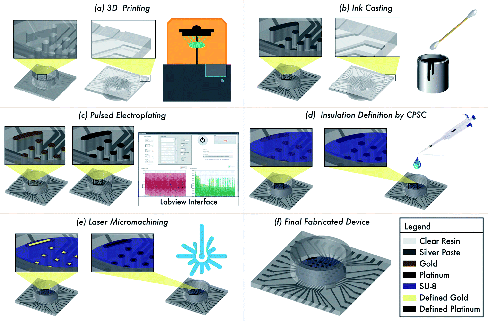 | ||
| Fig. 1 Schematic of the fabrication process involving (a) 3D printing, (b) ink casting, (c) pulsed electroplating, (d) lamination by CPSC, and (e) laser micromachining. (f) Schematic of final fabricated device with either nano-gold or nano-porous platinum microelectrodes. | ||
The unique non-planar design allows for monolithic integration of the culture well as the metallization of the traces via ink casting can be performed on the bottom side and the conductive ink transitions to the top side through the vias to yield electrodes on the topside of the MEA. With optimized printing conditions the diameter of an open via which can be successfully printed in a 1–1.5 mm thick die is 400–500 μm.22 Additionally, the width and depth of the micro troughs have been determined to be 200–250 μm and 100–150 μm respectively for successful ink casting in the subsequent steps.22 It is important to note here that electrode densities beyond a 2 × 2 array require traces to be routed through the spacing between the central electrode vias. For a 5 × 5 array, traces 250 μm wide connect the microelectrodes to the landing pads on the chip periphery. The minimum edge to edge separation between traces is 100 μm for a 5 × 5 design. Increasing the packing density even further to a 6 × 6 array, the minimum distance between the edges of adjacent traces is reduced to 60 μm while maintaining the similar width for the traces. Reducing the distance even further will not only result in print failures but also increase the chances of adjacent traces to result in a shorted connection upon ink casting. Through different routing schemes, we have observed that a 6 × 6 electrode array is the limit before multiple layers of routing have to be employed to connect all the electrodes to the periphery of the chip.
To achieve an even higher packing density, adjacent traces have to be routed even closer to each other. The increased density improves the spatial and temporal resolution of the MEA device. With proper design and optimization of the makerspace processes and materials, a packing density as high as 8 × 8 can be achieved. As the distance between the traces cannot be reduced below 60 μm for successful printing, this either forces an increase in the spacing between the electrode vias or movement of some traces to a separate layer. An increase in the spacing between the microelectrodes will not only increase the chip size but also decrease the spatial resolution of the MEA. Thus, for an 8 × 8 design traces for 16 electrodes have been transitioned to the top surface of the MEA while the remaining 48 traces are routed at the bottom. The 16 electrodes on the top surface can be visualized as a 4 × 4 matrix with trace dimensions similar to that on the bottom side. As the 8 × 8 MEA design has traces on both sides of the chip, the culture well is printed separately and affixed together with a biocompatible epoxy. For an 8 × 8 design, the number electrodes on the top side is significantly smaller than the bottom side, the traces can be routed in a manner such that the minimum edge to edge distance of 60 μm is not necessary. As the traces for the electrodes on the top side run on the top surface of the chip, the 16 electrodes are not printed as through vias. The depth of the electrodes in this case is 250 μm, which is similar to the depth of the traces. This additionally demonstrates the immense design flexibility offered by our process technology as it allows for rapid design changes.
Fig. 2(a) and (b) shows the bottom and top views of the SolidWorks model for a 6 × 6 array. Fig. 2(c) shows the Preform model with the scaffolding that are added around edges to support the device while printing and to prevent any deformation that can result from the printing process. Multiple devices can be added to the print bed to create several MEAs in a parallel fashion (up to a ∼6 inch × ∼6 inch substrate). The print time is primarily dependent on device height, so adding multiple devices to the print bed does not increase the print time. This is advantageous for batch fabrication of these devices. Fig. 2(d) and (e) shows the bottom and top views of the printed device. For the 8 × 8 MEA design, which has traces on both sides of the chip, the culture well is printed separately and affixed together with a biocompatible epoxy [Fig. 2(f)] similar to what we have reported earlier.22
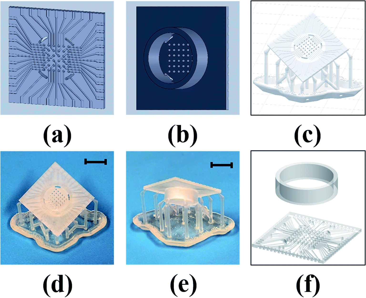 | ||
| Fig. 2 Stages of MEA fabrication: (a and b) SolidWorks model (bottom and top views of 6 × 6 design), (c) Preform model, (d and e) printed device (bottom and top views) and (f) 8 × 8 design in which the MEA chip and culture well are printed as two separate parts and affixed together with a biocompatible epoxy. Scale bars in (d) and (e) correspond to 10 mm. | ||
Throughout the process, the design had to be iteratively optimized to increase the density of the microelectrodes in the fabrication process. Due to the nature of additive manufacturing, these changes were simple to implement as necessary. One important design choice was to fabricate filled, conductive vias to connect the electrodes and traces on two opposite sides of the MEA chip. Another major design feature was to add the culture well on the top side of the MEA with the electrodes. Having the culture well connected to the MEA device allows co-design and fabrication of an important device fixture typically added as a separate feature during assembly steps. Such assembly steps are completely avoided in this approach with co-design and fabrication of the device and the package. It also leads to the benefit a reliably leak-proof MEA device.
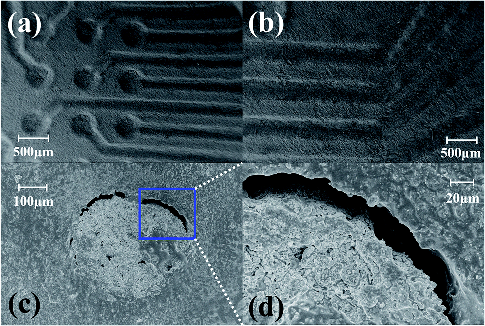
When adjusting the design in SolidWorks, the difference in dimensions between printed parts and their models had to be considered. Although the electrodes were modelled to 500 μm in diameter, they resolved at approximately 450 μm as seen in Fig. 3(a). A similar offset of 50 μm was also observed for the reference electrodes which printed 450 μm wide and 1250 μm long in contrast to design values of 500 μm and 1300 μm respectively [Fig. 3(b)]. For the traces the design to device offset was measured to be approximately 10 μm as the printed width was measured at 240 μm compared to a design value of 250 μm. The reduced design to device variation in the traces as compared to the vias is attributed to the depth of the features (150 μm versus 1.4 mm for the vias). The larger depth would correspond to more layers being 3D printed adding to the probability of print defects resulting in larger offsets for the additional printed layers. This offset needs to be considered with modeling features that are either small or in close proximity. As an example, adjacent traces become closer as we continue to increase the electrode density. This design to device offset can potentially increase the probability of neighboring traces shorting together. The limit that we have experimentally observed is to allow 80 μm between the traces during the design process in order to avoid having the traces short together.
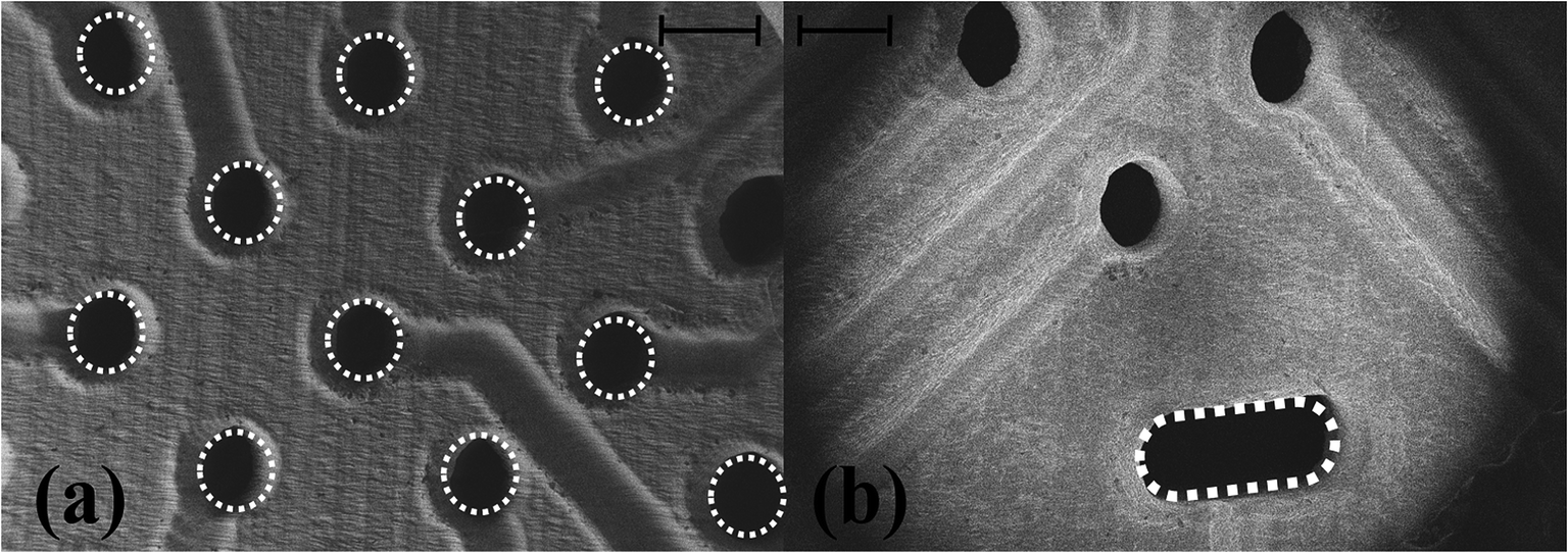 | ||
| Fig. 3 (a) SEM image of the vias and traces and (b) reference electrodes after 3D printing showing a reduced design to device offset of approximately 50 μm. The diameter of the dotted circles is 450 μm. The length and width of the dotted reference electrode is 450 μm wide and 1250 μm long. The width of the micro troughs for subsequent ink casting is measured as 240 μm showing a design to device offset of ∼10 μm. Scale bars in figures corresponds to 500 μm. | ||
2.2 Ink casting optimization
The ink casting process when performed using the manual casting method is repeatable. The viscosity of the paste was observed to be a very important factor to properly fill the 3D printed micro-troughs for the traces. A silver ink with lower viscosity (25000–45000 cP (ref. 33)) created difficulties in the ink casting process. Switching to a silver ink with higher viscosity (190000 cP (ref. 34)) allowed for better results. In order to optimize the bake time and temperature, the devices were monitored periodically for resistance and extent of cure. The devices were probed and resistance measurements from the contact pad to the electrode were recorded in DC conditions using a multimeter (Keithley 2400 Source Meter; Keithley Instruments, Cleveland, OH, USA). If the probe affected the silver ink, the device was not fully cured. The ink can be cured for a shorter period of time at a higher temperature, but it increases the thermal budget of the process and results in device warpage.22 Due to the design choice of the trace depth (150 μm), the sanding when done carefully does not affect the conductivity in the traces. When depth of the microtroughs for the traces is not optimum, reduced deposition of the ink causes possible trace removal during the sanding process. The optimal design choice of 150 μm deep microtroughs additionally enabled an IPA rinse step to remove any silver dust particles that result from the sanding process. At this step, silver meso-scale electrodes of 500 μm diameter are created and can be used as MEAs.
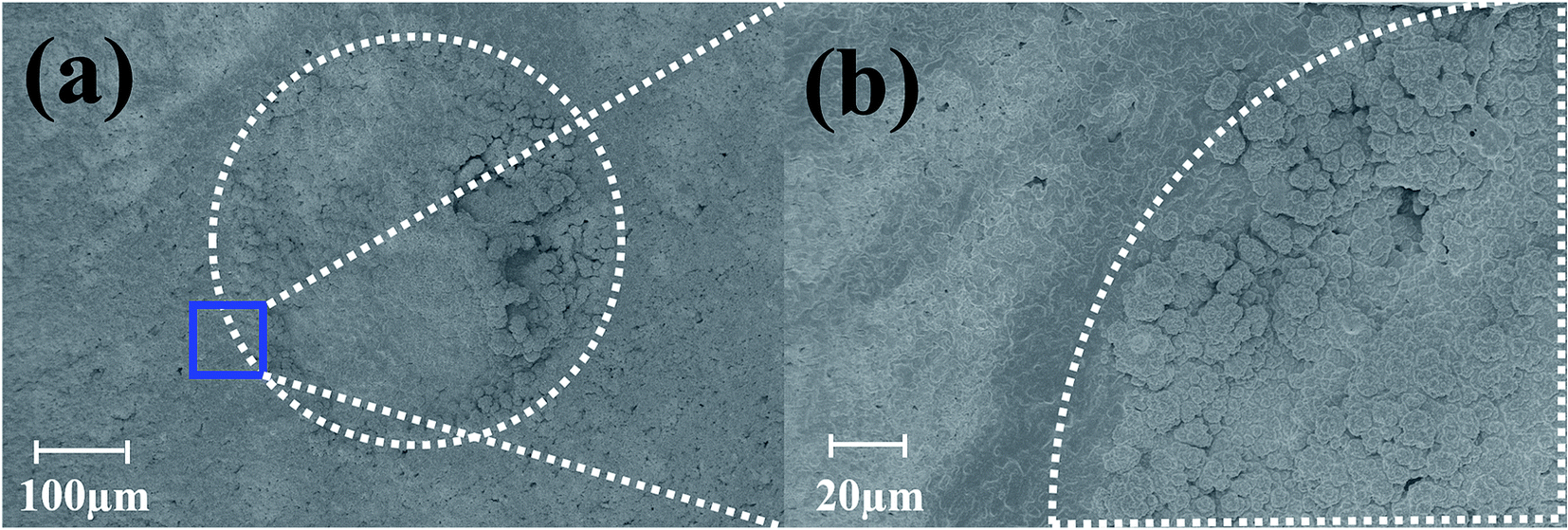
Fig. 4(a) depicts the photo micrograph of the bottom side for the ink-casted 5 × 5 device. It is observed that the ink casted traces run through the designed micro troughs without shorting adjacent electrodes. Further, it was observed that a minimum distance of 80 μm can be maintained between the traces without shorting them together in a photo micrograph of the bottom side of a 6 × 6 ink casted MEA device [Fig. 4(b)]. Fig. 4(c) and (d) show the top side containing 16 electrodes on an 8 × 8 MEA and the bottom side accommodating the remaining 48 electrodes. No evidence of shorting was observed in this repeatable process to produce an 8 × 8 grid of electrodes. SEM imaging of fabricated devices was performed to observe the electrodes and traces further in high magnification. SEM imaging confirms the optical micrograph results of the electrode vias transitioning to traces in a repeatable, uniform fashion [Fig. 5(a)] and no shorting between adjacent electrodes [Fig. 5(b)]. However, the electrical vias are not completely filled with the silver paste as seen in Fig. 5(c) and (d). This may be due to the shrinkage of the paste due to the evaporation of the solvents during the curing step.
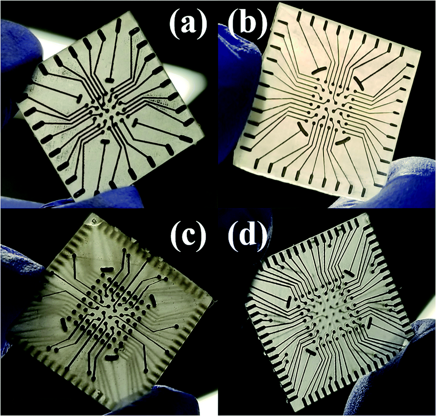 | ||
| Fig. 4 Optical micrographs of the bottom view of (a) 5 × 5 and (b) 6 × 6 ink casted device. Top view or 8 × 8 ink casted device showing (c) 16 electrodes on the top side and (d) 48 electrodes on the bottom side. Scale bar in figures correspond to 10 mm. | ||
 | ||
| Fig. 5 (a) SEM imaging depicting the microelectrodes transitioning smoothly to the traces as seen from the bottom side of the MEA chip. (b) Adjacent traces separated by a gap of ∼80 μm. SEM image of ink casted electrodes with (c) unfilled electrode edges and (d) close up of (c). | ||
2.3 Pulsed electroplating optimization
Pulsed electroplating allows for greater control over the nanomaterial properties of the planar MEA.35 Further, as silver is cytotoxic,27,28 the meso-scale electrodes can be selectively encapsulated with a biocompatible metal. The additive manufacturing process of pulsed electroplating provides improved biocompatibility, high level of control over the microelectrode properties, including matching of properties across the microelectrodes in the MEAs. Two different metals with favorable properties were electroplated: in addition to be very inert and biocompatible, platinum is a hard metallic layer and corrosion resistant making it good option as a microelectrode material36 and gold is conductive, wear resistant and biocompatible.37 DC plating is a simple process to set up but results in poor coverage and adhesion to the underlying materials.35 However, pulsed electroplating causes an increased nucleation rate leading to the formation of finer grains resulting in a controlled and adjustable process for biocompatible material definition with improved adhesion.38,39 The time of pulsed electroplating needs careful optimization and a clear effect of the plating time on the plating quality is observed in Fig. 6(a–f). At the higher end of the electroplating time spectrum (120 seconds) for both platinum and gold, the metal layer is clearly over plated as seen in Fig. 6(e) and (f). At the lower end of the time spectrum (40 seconds), the unfilled areas of the electrode vias which occurred due to the shrinkage of the silver paste do not completely fill the edges of the vias and this effect is observed for both platinum and gold electroplating more clearly during SEM imaging. An optimized electroplating time of 60 seconds was sufficient to fill the edges of the vias as observed in the SEM images of Fig. 7(a) and (b). Fig. 8(a) shows SEM image of a silver electrode with an optical photo micrograph in the inset. Fig. 8(b) and (c) depict SEM images of the nano-porous platinum and nano-structured gold microelectrodes respectively. The nanoscale topography of both the materials is clearly observed for these images. ImageJ analysis40 of the SEM topographies indicates a ∼13% and ∼25% porosity of the electroplated nano-porous platinum and nano-gold respectively. This is evidence of an optimized pulsed electroplating process as opposed to rougher deposits of metal, a characteristic of DC electroplating.38,39 Our observations hold for the full MEA device.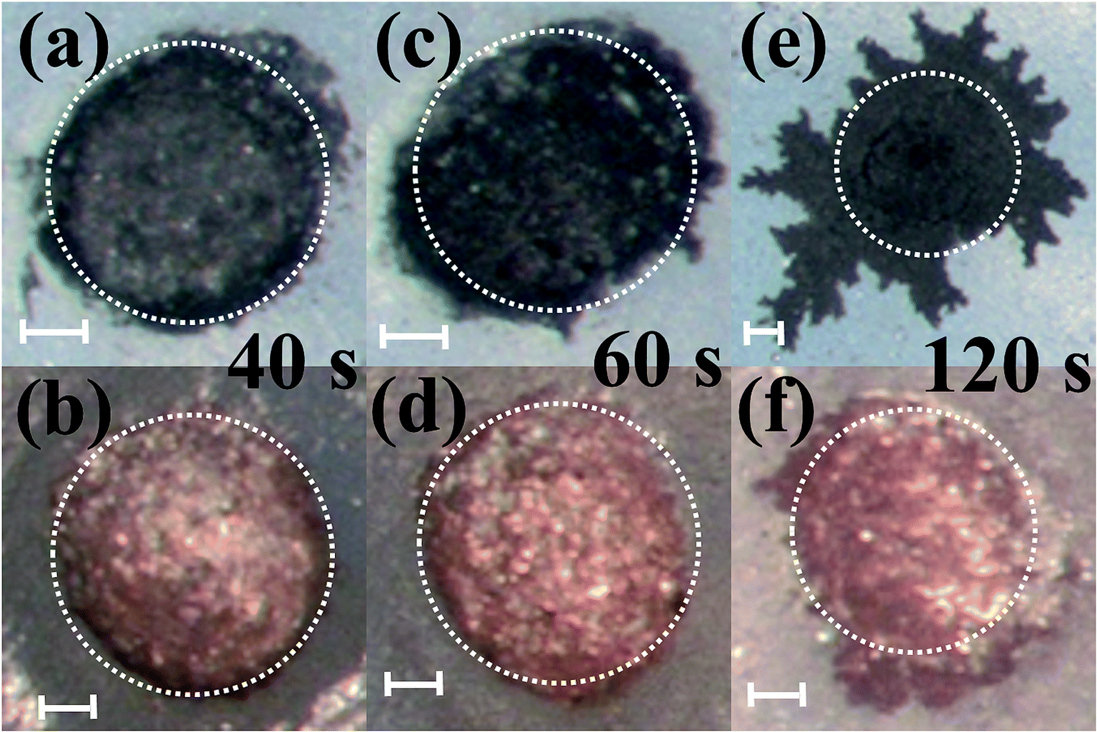 | ||
| Fig. 6 Comparison of different electrodes plated for varying amounts of time with the same current density. Top and bottom rows of images correspond to platinum and gold electroplating respectively. Time of electroplating: (a and b) 40 seconds, (c and d) 60 seconds and (e and f) 120 seconds. Scale bars on figure correspond to 100 μm. | ||
 | ||
| Fig. 7 (a) SEM images depicting pulsed electroplated platinum atop the silver ink casted electrodes with (b) depicting filling of the electrode edges. | ||
 | ||
| Fig. 8 SEM images of (a) silver electrodes with photo micrograph of ink casted silver electrode as inset (scale bar of the inset image corresponding to 100 μm), (b) nano-porous platinum electrode, and (c) nano-gold electrodes. (d) SU-8 CPSC MEA device after platinum electroplating showing a conformal layer of uniform insulation. | ||
2.4 Confined precision spin coating (CPSC) and laser micromachining optimization
In order to enable biocompatibility and transition the meso-scale electrodes to microelectrodes, the inside of the culture well is coated utilizing a newly developed insulation technology. This method has been named Confined Precision Spin Coating (CPSC). The unique non-planar design of the MEA allows for a major advantage during the insulation definition process. As the traces for the electrodes are on the bottom side for most designs, a planar and conformal coating on the electrodes in the top side are obtained after CPSC. The spin coating process not only covers the electrodes but also the inner walls of the culture well so that the 3D printed resin does not come in contact with the cell culture media or the cells. Allowing the SU-8 to spread inside culture well manually before spin-coating, the CPSC method, resulted in a more uniformly thin insulation layer (4 ± 1 μm).41 Fig. 8(d) shows the SEM image of the SU-8 cast MEAs with a conformal and uniform layer of insulation.As already discussed the pulsed electroplated platinum and gold layers have nanoscale topographies and MATLAB® analysis of Fig. 8(b) and (c) indicate that the electroplated platinum layer has an average pore radius of 400 nm as compared to the average pore radius of 600 nm for the electroplated gold. Fig. 9(a) and (b) shows the relative frequency of different pore radii of the pulse electroplated platinum and gold layers respectively. Although the average pore radius of both the layers are moderately comparable, the increased porosity of the gold layer over the platinum layer (∼25% for Au as compared to ∼13% for Pt) would result in higher effective surface area when compared to the geometric area of the microelectrode.
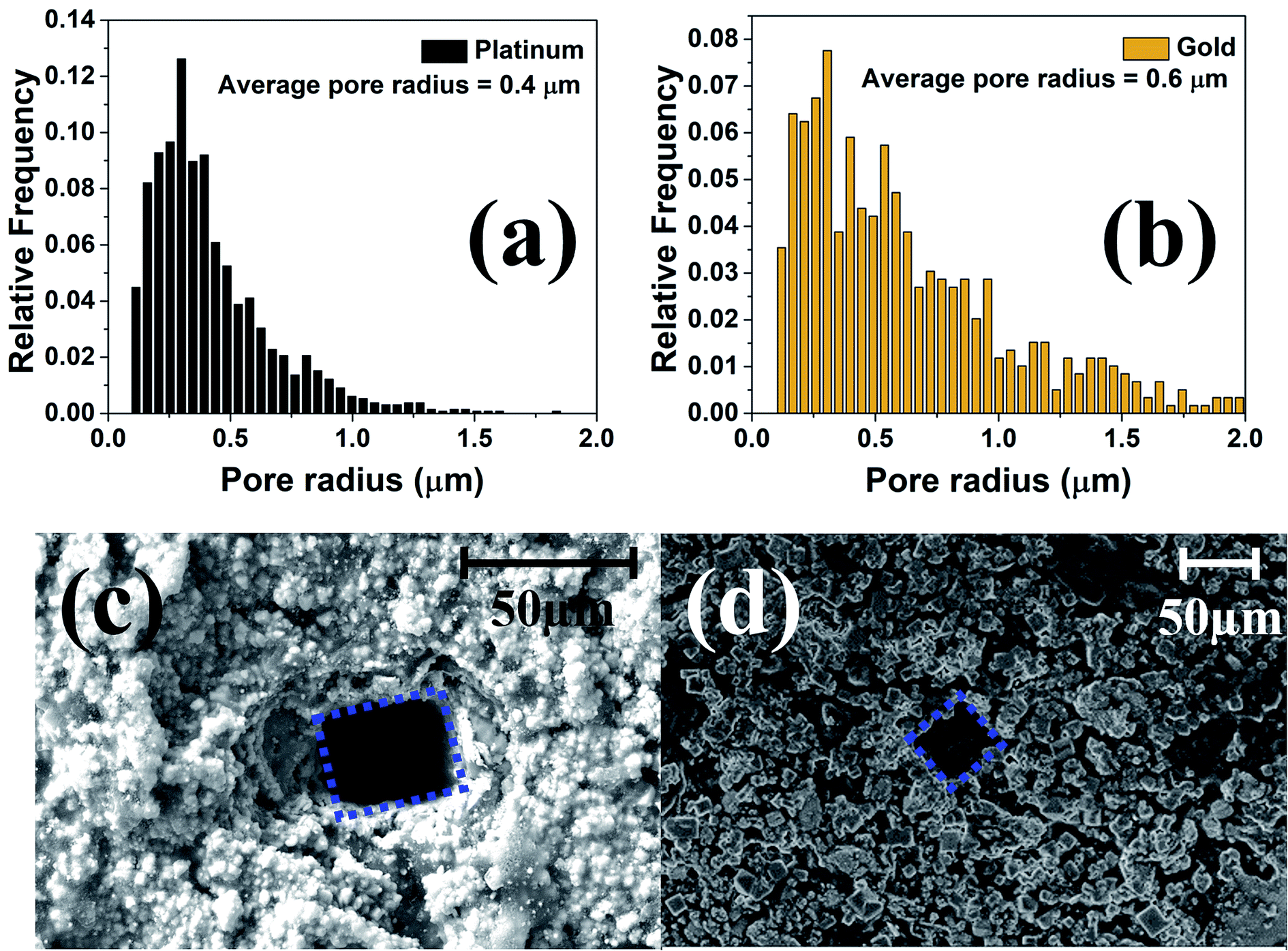 | ||
| Fig. 9 Pore size distribution of the (a) nano-porous platinum and (b) nano-gold layers. SEM image of laser micromachining on (c) SU-8 CPSC over platinum and (d) SU-8 CPSC over gold. The defined microelectrode of ∼50 μm × 50 μm area is outlined. | ||
Laser micromachining of the SU-8 layer enables the definition of the recording sites on the meso-scale electrodes after CPSC to realize the microelectrodes. The laser micromachining is performed, after CPSC and fully cross linking the material, to selectively define nano-porous platinum [Fig. 9(c)] and nano-gold [Fig. 9(d)] microelectrodes of 50 μm × 50 μm size in the SU-8 layer. It is worth noting that the electroplating process performed after CPSC and laser ablation, resulted in limited success with the plating process. We believe this is due to surface hydrophobicity and liquid tension that impede the electroplating solution from gaining access to the recording site. Switching the electroplating process to before insulation definition allowed for reliable fabrication of plated electrodes. Fig. 10(a–c) show the final fabricated devices from previously reported 3 × 3 array22 to a monolithically integrated 6 × 6 array and a standard, commercial density 8 × 8 MEA.
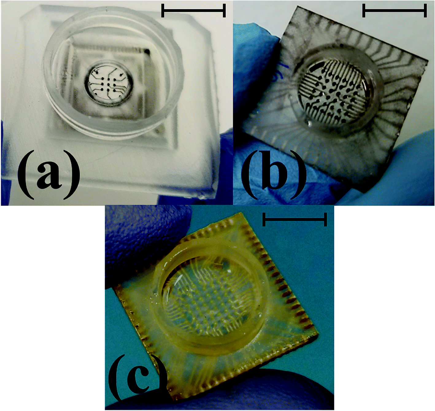 | ||
| Fig. 10 Optical images of the final fabricated device ready for testing transitioning from the previously reported 3 × 3 array22 (a) to a monolithically integrated 6 × 6 array (b) and a high density 8 × 8 array MEA (c). Scale bar in the images corresponds to 10 mm. | ||
2.5 Characterization
For characterization of these device, a full spectrum impedance measurements were performed. The full spectrum impedance allows for a complete view of the impedance of the device at different frequencies. Microelectrode noise is directly proportional to the square root of the real part of the impedance value and as a result, a low noise electrode implies a low impedance value and improved signal to noise (SNR) during signal acquisition (voltage measurements) in electrophysiology.42,43 From the resistance measurements performed at DC during ink casting, the conductivity was already observed to be consistently excellent due to an average resistance of 4.46 Ω with a standard deviation of 4.9 mΩ (N = 25). Fig. 11(a) shows the full spectrum impedance of the silver ink casted, nano-porous platinum, and nano-gold electrodes prior to insulation definition (meso-scale electrodes). It is observed that the impedance values at the electrophysiologically significant frequency of 1 kHz (ref. 42 and 43) decreases significantly after pulsed electroplating of either metal.44 Fig. 11(b) depicts the full spectrum impedance of gold and platinum electrodes after laser micromachining of the SU-8 insulation. As the electrode size is now 50 μm × 50 μm, the impedance at 1 kHz increases significantly because the electrode impedance is inversely proportionally to the geometric size of the electrode.45 Specifically, the nano-porous platinum microelectrodes exhibit an average impedance of 36.8 kΩ at 1 kHz (N = 3) while the nano-gold microelectrodes show an average impedance of 16 kΩ at 1 kHz (N = 3). Fig. 11(c) depicts the phase response (in degrees) of the fabricated MEAs. An equivalent electrical circuit based on the well-established Randles impedance model46,47 was developed (Fig. 11(b–d)). Using this model, key circuit components of the fabricated MEAs were extracted. The extracted circuit elements have been represented in Fig. 11(d) and the analytically obtained curves for impedance and phase spectra have been presented along with the experimentally obtained values in Fig. 11(b) and (c). It is observed that the increased porosity of the gold electrode results in lower RCT values for the nano-gold MEAs as RCT is inversely proportional to the surface area of the electrode.47 This causes the impedance spectral of the nano-gold MEAs to be lower than the nano-porous platinum MEAs in the very low frequency regime (∼100 Hz). The increased porosity of the nano-gold MEAs also results in higher CDL (520 nF cm−2) when compared to CDL value of 400 nF cm−2 for the nano-porous platinum MEAs. The presence of the Warburg element48 is observed in both the MEAs with similar values of solution resistance (RS).49 The phase spectrum as observed in Fig. 11(c) has shifted from −60° to near 0° with an increase in frequency which implies that the overall characteristics of the electrode–electrolyte interface is governed by the double layer capacitance (CDL) at mid-range of frequencies (102–105 Hz) and becomes more resistive at higher frequencies (>105 Hz) as the solution resistance of the electrolyte begins to dominate the electrode–electrolyte interfacial impedance as it has been observed with other reported MEAs.46,49 For comparison, typical 2D MEAs fabricated in a cleanroom having similar sizes have a high impedance (real part) at lower frequencies and decrease in impedance as the frequency increases with an impedance of 20–40 kΩ at the electrophysiologically significant frequency of 1 kHz.15,42,43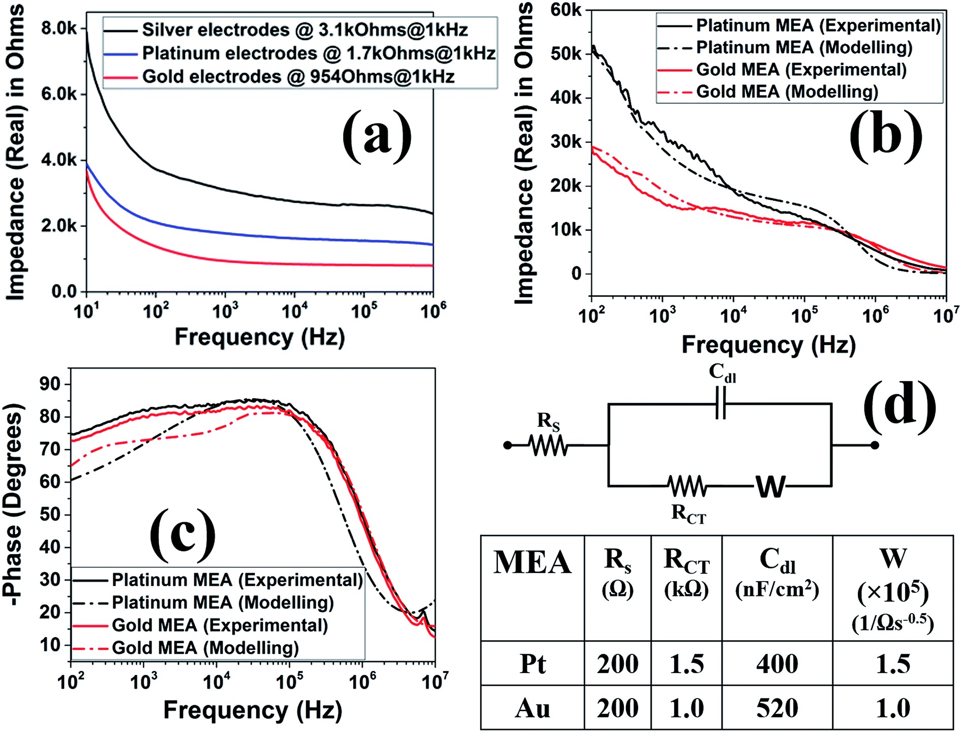 | ||
| Fig. 11 Full spectrum impedance graphs for (a) 450 μm diameter electrodes and (b) 50 μm × 50 μm laser micromachined electrodes (as obtained experimentally and by modelling), (c) phase (degrees) of the 50 μm × 50 μm laser micromachined electrodes (as obtained experimentally and by modelling). (d) Randles equivalent model used for extraction of the MEA circuit elements and the estimated values for the nano-porous platinum and nano-gold MEAs. | ||
2.6 Comparison of the glass MEAs and 3D printed MEAs
A manufacturing technology-based comparison of glass MEAs and planar, additive manufacturing based MEAs was performed to understand whether AM technologies can compete with traditional silicon/glass MEMS technologies with respect to various feature sizes. Fig. 12 represents the comparison of the deviations in dimensions of glass MEAs and 3D printed MEAs (values represent an average of N = 3 devices for both MEA types). The values show the relative deviation of the measured average from the designed dimension. Measurements of dimensions of microelectrodes, reference electrodes, traces, contact pads and SU-8 openings were performed. The relative deviation of the measured average from the expected design values were determined to achieve a comparison of the two technologies. The data represents less than 5% deviation from design for the 3D printing-based approach in more than the half of the categories that were measured, which is comparable to the glass approach. The 3D printing-based process compares very favorably in terms of design to device with traditional glass-based cleanroom processes while representing a dramatic reduction in cost, timeline for fabrication, reduction in the number of steps and the need for sophisticated equipment. A technological summary comparing the two technologies is conducted in Table 1, where it is observed that the additive manufacturing approach compares favorably with the traditional approach in environment, number of process steps, time, cost and equipment/materials. Resolution of cleanroom-based approaches is superior but laser micromachining and advanced 3D printing technologies50,51 can bridge the gap between both technologies even in this space. Furthermore, both fabrication techniques use SU-8 as insulation, which is self-planarizing and it reduces surface roughness issues.52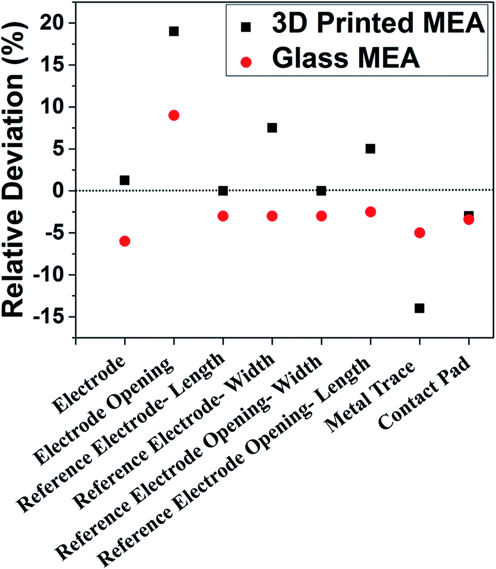 | ||
| Fig. 12 Comparison of the deviations in dimensions of glass micromachined and 3D printed MEAs (values represent a measured average of N = 3 devices for both MEA types). The values show the relative deviation from the measured average to the designed dimension. | ||
| Glass micromachining | 3D printed | |
|---|---|---|
| a Laser micromachining (QuickLaze 50ST2, Eolite Lasers, Portland, OR, USA).b Nanoscribe GmbH (Nanoscribe, Eggenstein-Leopoldshafen, Germany).c Asiga Digital Light Processing (DLP) 3D printer (MAX X27); (Asiga, Sydney, Australia). | ||
| Environment | Cleanroom | Makerspace/benchtop |
| Process steps | >10 | <10 |
| Resolution | <1 μm | ∼2 μma,b, ∼27 μmc |
| Total time | Upto 4 months | ∼4 days |
| Cost | $$$$ | $ |
| Fabrication equipment | Mask aligner, fumehood, spinner, hot plate, wirebonder, die attach, E-beam evaporator, mask maker/high res. printer, dicing saw, etc. | 3D printer, oven, UV-lamp, micromill, laser, spinner, benchtop sputterer or E-beam evaporator, current source |
| Backend equipment | Yes | None |
| Materials | Glass wafer, photoresist, photo mask, metal pellets/metal target, insulation, solvents, PCB, gold wire, etc. | 3D printing resin, isopropanol, stencil mask, conductive ink, electroplating materials, insulation |
3. Experimental
3.1 Design and 3D printing
The total die size is 19.5 mm × 19.5 mm × 1 mm to maintain compatibility with the Axion BioSystems (Atlanta, GA, USA) commercial MUSE electronics (Axion BioSystems, Atlanta, GA, USA) and AxIS software (version 2.3, Axion BioSystems, Atlanta, GA, USA). After choosing a desired electrode density and a routing strategy, SolidWorks (SolidWorks 2017; Dassault Systèmes, Waltham, MA, USA) was used to realize the design. The design file is then converted in the software PreForm (PreForm Software 2.16.0; Formlabs, Somerville, MA, USA) to orient and add support structures to the model for printing. The model is subsequently printed (Form 2; Formlabs, Somerville, MA, USA) using a clear resin (Clear Resin FLGPCL04; Formlabs, Somerville, MA, USA). After the print is completed, the support structures are removed from the print bed and the devices are soaked in isopropyl alcohol (70% IPA; Thermo Fisher Scientific Inc., Waltham, MA) for 10 minutes. The rinse process is repeated again in a fresh IPA bath to remove any uncured resin.3.2 Ink casting
Once the MEA framework is subject to a drying process using a nitrogen gun, silver nanoparticle ink (PRIMA-SOLDER™ EG8050; AI Technology, Princeton Junction, NJ, USA) is added to the bottom side of the device. The ink is deposited evenly using a cotton swab and excess ink is removed. The ink removal is carefully controlled in order to reduce the probability of loss of conductivity of the traces. After casting the ink, the device is cured in an oven (Precision Compact Oven; Thermo Fisher Scientific Inc., Waltham, MA, USA). The optimal curing time at 45 °C was 24 hours. Upon removal from the oven, the top side of the ink cast MEA was sanded (UEETEK Dry Wet Waterproof Sandpaper Sheets 1000 Grit) to get rid of any excess silver and prevent and shorting of traces.3.3 Pulsed electroplating
Electroplating solution of either gold (TSG 250; Transene Company Inc., Danvers, MA, USA) or platinum (hexachloro platinic acid with HCl and Lead Acetate, as defined in our prior work22) is added into the culture well and a platinum wire, used as the counter electrode, is inserted into the solution. The gold electroplating solution was pre-heated to 80 °C in a glass beaker prior to being transferred to the culture well. The current and voltage control that is required to perform electroplating was performed using a programmed Source Meter with two probes (Keithley 2400 Source Meter; Keithley Instruments, Cleveland, OH, USA). One of the probes is connected to the cathode which is attached to a piece of copper tape (Copper tape; Tapes Master, Monterey Park, CA, USA) shorting all of the contact pads of the device together and the other probe is connected to the anode. The Keithley 2400 Source Meter was programmed to have a graphical user interface using Labview (LabVIEW NXG 2.1; National Instruments, Austin, TX, USA) to conduct waveform specific electroplating. This process involved using an instrument driver and programming an example interface that can serve to input the electroplating parameters. The final executable program, allows for adjustment of process parameters such as duty cycle, source amplitude, pulse time, number of pulses, compliance amplitude, and waveform type (pulsed or constant). The chosen process parameters are entered into the LabView executable program, for implementing the electroplating process sequence. After process development a final recipe was developed consisting of a square wave pulse having a duty cycle of 50% was chosen with a current density of 1 A cm−2. The voltage compliance amplitude was set at 10 V and the electroplating was performed for 40 seconds, 60 seconds and 120 seconds for both platinum and gold. After the desired electroplating time, the Source Meter automatically stops and the probes are disconnected from the device. Additionally, the plating solution is removed and the culture well is rinsed with DI water and IPA.3.4 CPSC process development
A 60 μL drop of SU-8 (SU-8 GM 1050; Gersteltec, Pully, Switzerland) is added into the culture well and spin-coated (G3P-8 Coater; Specialty Coating Systems, Inc., Woodland Dr, Indianapolis, IN, USA) for 40 seconds at 2660 rpm. The SU-8 layer is subsequently cross linked for 10 minutes under a UV flood light (Loctite Zeta 7411 UV Flood Curing System; Loctite, Henkel Technologies, Düsseldorf Germany). This creates a thin layer of biocompatible insulation15 that will protect any cells from the undesired toxicity of the 3D printed resin. Additionally, this layer planarizes the top layer of the MEA and exhibits sufficient dielectric properties for reliable signal transmission during the use of the device in electrical, electrochemical and electrophysiological characterizations.3.5 Laser micromachining
A multi-modal laser micromachining tool (QuikLaze 50ST2; Eolite Lasers, Portland, OR, USA) is used to ablate through the SU-8 layer and define the recording sites (microelectrodes). The multi-modal laser was operated in the 50 Hz ultraviolet (UV) wavelength in order to ablate the SU-8 layer. Each square hole created by the laser, when being used in the UV mode with 100% aperture size, is 50 μm × 50 μm in size. To ablate all the way through the SU-8 layer, the laser is pulsed at an individual electrode using 100% aperture and 50% power with a burst of 2 shots (7.2 mJ).3.6 Measurements
Full spectrum impedance measurements of both meso-scale and microelectrodes were performed using a Bode 100 (Bode 100; Omicron Labs, Houston, TX, USA) for logarithmic frequency sweeps from 10 Hz to 10 MHz on each electrode with Phosphate Buffer Solution (PBS) (Dulbecco's Phosphate Buffer Solution; Thermo Fisher Scientific, Waltham, MA, USA) as the electrolyte and a platinum wire (Pt/Ti Wire Anode; eDAQ, Denistone East, Australia) as the counter electrode. Imaging of the devices was conducted with a Scanning Electron Microscope (SEM) (ULTRA-55 FEG SEM; Carl Zeiss, Oberkochen, Germany) and a stereomicroscope (SMZ800 Zoom Stereomicroscope; Nikon, Tokyo, Japan).4. Conclusions
We present a complete makerspace enabled fabrication of a single well 8 × 8 MEA for in vitro electrophysiology and biosensing applications. The reported process can result in rapid, robust, benchtop based, and design-to-device in a matter of 4 days as opposed to cost and time intensive, cleanroom-based approaches. The process is extremely cost-effective for MicroTAS and BioMEMS devices to be manufactured in low resource settings. A unique non-planar design approach for the microfabrication of the MEAs enables both silver ink casting without shorts and selective pulsed electroplating (another additive manufacturing process) of biocompatible electrode materials such as gold and platinum selectively on the microelectrodes. The non-planar design choice additionally helps in realizing a planar and conformal layer of SU-8 insulation by a Confined Precision Spin Coating (CPSC) technique. The culture well was integrated in the design of the device for most designs which allowed for monolithically 3D printing the entire device. The addition of the SU-8 insulation and electroplating of the electrodes with platinum/gold make the device biocompatible for in vitro applications. The fabricated 50 μm × 50 μm MEA having a maximum of 64 electrodes has an 1 kHz impedance of 36.8 kΩ/16 kΩ with a double layer capacitance of 400 nF cm−2/520 nF cm−2 for nano-porous platinum/nano-gold respectively which is comparable to the state-of-art commercially available 2D MEAs. We believe our results are very significant for the cell-based biosensors, environmental sensors and other communities since this technology can result in quick turnaround of ideas to a prototype that can be tested rapidly reducing cycle time between iterations and advancing the end applications such as toxicity screening and drug discovery.Conflicts of interest
We have one conflict of interest to disclose: Prof. Rajaraman is a co-founder of Axion BioSystems Inc., which designs, manufactures and sells planar, high-throughput MEAs. He has financial interests in the company but no active role in its operations.Acknowledgements
The authors would like to thank the National Science Foundation for support of this work through a Summer Research Experience Undergraduate (REU) program (site EEC 1560007) that supported Ms Crystal Nattoo. We would further like to thank Deutschen Akademischen Austauschdienstes (DAAD) in combination with PROMOS and resources of the Bundesministeriums für Bildung und Forschung (BMBF) Scholarships for supporting the undergraduate research studies of Ms Sandra Springer and Ms Sarah Fremgen. Additionally, we would like to thank the University of Central Florida (Orlando, FL, USA) start-up funding of Prof. Rajaraman for funding and the Materials Characterization Facility (MCF). Special thanks to Mr Charles Didier, Ms Nilab Azim and Ms Cacie Hart for providing any and all help in the laboratory.References
- V. Gomes, A. Barros, S. Martinoia, A. Pasquarelli and J. Swart, Fabrication of 60 channel microelectrode arrays for future use with cultured neuronal networks, in Microelectronics Technology and Devices (SBMicro), 2015 30th Symposium on, IEEE, 2015, pp. 1–4 Search PubMed.
- C. Hart, A. Kundu, K. Kumar, S. Varma, J. Thomas and S. Rajaraman, Rapid Nanofabrication of Nanostructured Interdigitated Electrodes (nIDEs) for Long-Term In Vitro Analysis of Human Induced Pluripotent Stem Cell Differentiated Cardiomyocytes, Biosensors, 2018, 8(4), 88 CrossRef PubMed.
- J. A. DiMasi, H. G. Grabowski and R. W. Hansen, Innovation in the pharmaceutical industry: new estimates of R&D costs, Journal of Health Economics, 2016, 47, 20–33 CrossRef PubMed.
- M. Chiappalone, A. Vato, M. Marcoli, F. Davide and S. Martinoia, Networks of neurons coupled to microelectrode arrays: a neuronal sensory system for pharmacological applications, Biosens. Bioelectron., 2003, 18(5–6), 627–634 CrossRef CAS PubMed.
- C. M. Woodard, B. A. Campos, S.-H. Kuo, M. J. Nirenberg, M. W. Nestor, M. Zimmer, E. V. Mosharov, D. Sulzer, H. Zhou and D. Paull, iPSC-derived dopamine neurons reveal differences between monozygotic twins discordant for Parkinson's disease, Cell Rep., 2014, 9(4), 1173–1182 CrossRef CAS PubMed.
- K. A. Jewett, C. A. Christian, J. T. Bacos, K. Y. Lee, J. Zhu and N.-P. Tsai, Feedback modulation of neural network synchrony and seizure susceptibility by Mdm2-p53-Nedd4-2 signaling, Mol. Brain, 2016, 9(1), 32 CrossRef PubMed.
- J. López-Erauskin, T. Tadokoro, M. W. Baughn, B. Myers, M. McAlonis-Downes, C. Chillon-Marinas, J. N. Asiaban, J. Artates, A. T. Bui and A. P. Vetto, ALS/FTD-Linked Mutation in FUS Suppresses Intra-axonal Protein Synthesis and Drives Disease Without Nuclear Loss-of-Function of FUS, Neuron, 2018, 816–830 CrossRef PubMed.
- Y. Yang, M. A. Mis, M. Estacion, S. D. Dib-Hajj and S. G. Waxman, Na V 1.7 as a Pharmacogenomic Target for Pain: Moving Toward Precision Medicine, Trends Pharmacol. Sci., 2018, 258–275 CrossRef PubMed.
- B. A. DeRosa, J. El Hokayem, E. Artimovich, C. Garcia-Serje, A. W. Phillips, D. Van Booven, J. E. Nestor, L. Wang, M. L. Cuccaro and J. M. Vance, Convergent Pathways in Idiopathic Autism Revealed by Time Course Transcriptomic Analysis of Patient-Derived Neurons, Sci. Rep., 2018, 8(1), 8423 CrossRef PubMed.
- E. Seker, Y. Berdichevsky, M. R. Begley, M. L. Reed, K. J. Staley and M. L. Yarmush, The fabrication of low-impedance nanoporous gold multiple-electrode arrays for neural electrophysiology studies, Nanotechnology, 2010, 21(12), 125504 CrossRef PubMed.
- H. Yang, M. T. Rahman, D. Du, R. Panat and Y. Lin, 3-D printed adjustable microelectrode arrays for electrochemical sensing and biosensing, Sens. Actuators, B, 2016, 230, 600–606 CrossRef CAS PubMed.
- D. A. Koutsouras, A. Hama, J. Pas, P. Gkoupidenis, B. Hivert, C. Faivre-Sarrailh, E. Di Pasquale, R. M. Owens and G. G. Malliaras, PEDOT: PSS microelectrode arrays for hippocampal cell culture electrophysiological recordings, MRS Commun., 2017, 7(2), 259–265 CrossRef CAS.
- H. Pan, X. Lü, Z. Wang, T. Ren, T. Fang, J. Zhang, C. Zhou and L. Wang, Silicon-based microelectrode arrays for stimulation and signal recording of in vitro cultured neurons, Sci. China Inf. Sci., 2011, 54(10), 2199 CrossRef.
- M. Welkenhuysen, L. Hoffman, Z. Luo, A. De Proft, C. Van den Haute, V. Baekelandt, Z. Debyser, G. Gielen, R. Puers and D. Braeken, An integrated multi-electrode-optrode array for in vitro optogenetics, Sci. Rep., 2016, 6, 20353 CrossRef CAS PubMed.
- C. Karnati, R. Aguilar, C. Arrowood, J. Ross and S. Rajaraman, Micromachining on and of transparent polymers for patterning electrodes and growing electrically active cells for biosensor applications, Micromachines, 2017, 8(8), 250 CrossRef PubMed.
- J. Yang and D. C. Martin, Microporous conducting polymers on neural microelectrode arrays: II. Physical characterization, Sens. Actuators, A, 2004, 113(2), 204–211 CrossRef CAS.
- A. Blau, A. Murr, S. Wolff, E. Sernagor, P. Medini, G. Iurilli, C. Ziegler and F. Benfenati, Flexible, all-polymer microelectrode arrays for the capture of cardiac and neuronal signals, Biomaterials, 2011, 32(7), 1778–1786 CrossRef CAS PubMed.
- J. Ross, E. A. Brown, S. Rajaraman, M. G. Allen and B. Wheeler, Apparatus and methods for high throughput network electrophysiology and cellular analysis, Utility Patent, US9290756B2, 2016.
- N. Adly, S. Weidlich, S. Seyock, F. Brings, A. Yakushenko, A. Offenhäusser and B. Wolfrum, Printed microelectrode arrays on soft materials: from PDMS to hydrogels, Flexible Electron., 2018, 15 CrossRef.
- Y. Khan, M. Garg, Q. Gui, M. Schadt, A. Gaikwad, D. Han, N. A. Yamamoto, P. Hart, R. Welte and W. Wilson, Flexible hybrid electronics: direct interfacing of soft and hard electronics for wearable health monitoring, Adv. Funct. Mater., 2016, 26(47), 8764–8775 CrossRef CAS.
- D. I. Walsh III, D. S. Kong, S. K. Murthy and P. A. Carr, Enabling microfluidics: from clean rooms to makerspaces, Trends Biotechnol., 2017, 35(5), 383–392 CrossRef PubMed.
- A. Kundu, T. Ausaf and S. Rajaraman, 3D Printing, Ink Casting and Micromachined Lamination (3D PICLμM): A Makerspace Approach to the Fabrication of Biological Microdevices, Micromachines, 2018, 9(2), 85 CrossRef PubMed.
- D. Pranzo, P. Larizza, D. Filippini and G. Percoco, Extrusion-Based 3D Printing of Microfluidic Devices for Chemical and Biomedical Applications: A Topical Review, Micromachines, 2018, 9(8), 374 CrossRef PubMed.
- M. Sharafeldin, A. Jones and J. F. Rusling, 3D Printed Biosensor Arrays for Medical Diagnostics, 2018 Search PubMed.
- I. Gibson, D. W. Rosen and B. Stucker, Photopolymerization processes, in Additive Manufacturing Technologies, Springer, 2010, pp. 78–119 Search PubMed.
- J. Schnitker, N. Adly, S. Seyock, B. Bachmann, A. Yakushenko, B. Wolfrum and A. Offenhäusser, Rapid Prototyping of Ultralow-Cost, Inkjet-Printed Carbon Microelectrodes for Flexible Bioelectronic Devices, Adv. Biosyst., 2018, 2(3), 1700136 CrossRef.
- P. AshaRani, G. Low Kah Mun, M. P. Hande and S. Valiyaveettil, Cytotoxicity and genotoxicity of silver nanoparticles in human cells, ACS Nano, 2008, 3(2), 279–290 CrossRef PubMed.
- S. Meryon and A. Brook, In vitro comparison of the cytotoxicity of twelve endodontic materials using a new technique, Int. Endod. J., 1990, 23(4), 203–210 CrossRef CAS PubMed.
- S. Arora, J. Jain, J. Rajwade and K. Paknikar, Cellular responses induced by silver nanoparticles: in vitro studies, Toxicol. Lett., 2008, 179(2), 93–100 CrossRef CAS PubMed.
- A. Carnicer-Lombarte, H. T. Lancashire and A. Vanhoestenberghe, In vitro biocompatibility and electrical stability of thick-film platinum/gold alloy electrodes printed on alumina, Journal of Neural Engineering, 2017, 14(3), 036012 CrossRef PubMed.
- S. Rajaraman, J. D. Ross and A. Preyer, Devices, systems and methods for high-throughput electrophysiology, Utility Patent, US20150027885A1, 2016.
- S. Rajaraman, J. D. Ross and A. Preyer, Devices, systems and methods for high-throughput electrophysiology, US Patent App. 14/744,513, 2015.
- E. T. Inc, EPO-TEK® EJ2189-LV - Epoxy Technology, available: http://www.epotek.com/site/administrator/components/com_products/assets/files/Style_Uploads/EJ2189-LV.pdf.
- I. AI Technology, EG8050 - AI Technology, Inc., available: https://www.aitechnology.com/uploads/pdf/products/nasa/eg8050t.pdf.
- C. Seah, S. Mridha and L. Chan, DC/pulse plating of copper for trench/via filling, J. Mater. Process. Technol., 2001, 114(3), 233–239 CrossRef CAS.
- S. P. Experts. Platinum, available: https://www.sharrettsplating.com/coatings/platinum.
- S. T. Experts. Gold, available: https://www.sharrettsplating.com/coatings/gold.
- J.-C. Puippe and F. Leaman, Theory and practice of pulse plating, Amer Electroplaters Soc, 1986 Search PubMed.
- U. Erb, Electrodeposited nanocrystals: synthesis, properties and industrial applications, Nanostruct. Mater., 1995, 6(5–8), 533–538 CrossRef.
- https://imagej.nih.gov/ij/.
- G. E. Solutions. GM1050 for layers between 3-8μm, available: http://www.gersteltec.ch/userfiles/GM1050_v1.0.pdf.
- D. Borkholder, J. Bao, N. Maluf, E. Perl and G. Kovacs, Microelectrode arrays for stimulation of neural slice preparations, J. Neurosci. Methods, 1997, 77(1), 61–66 CrossRef CAS PubMed.
- D. Borkholder, Cell based biosensors using microelectrodes, Stanford University, 1998 Search PubMed.
- C. f. N. Education, Conductivity and Resistivity Values for Misc. Materials, http://https://www.ndeed.org/GeneralResources/MaterialProperties/ET/Conductivity_Misc.pdf.
- S. Rajaraman, S.-O. Choi, M. A. McClain, J. D. Ross, M. C. LaPlaca and M. G. Allen, Metal-transfer-micromolded three-dimensional microelectrode arrays for in vitro brain-slice recordings, J. Microelectromech. Syst., 2011, 20(2), 396–409 Search PubMed.
- R. Wang, X. Huang, G. Liu, W. Wang, F. Dong and Z. Li, Fabrication and characterization of a parylene-based three-dimensional microelectrode array for use in retinal prosthesis, J. Microelectromech. Syst., 2010, 19(2), 367–374 CAS.
- N. Joye, A. Schmid and Y. Leblebici, Electrical modeling of the cell–electrode interface for recording neural activity from high-density microelectrode arrays, Neurocomputing, 2009, 73(1–3), 250–259 CrossRef.
- A. Ledo, C. t. F. Lourenço, J. o. Laranjinha, C. M. Brett, G. A. Gerhardt and R. M. Barbosa, Ceramic-based multisite platinum microelectrode arrays: morphological characteristics and electrochemical performance for extracellular oxygen measurements in brain tissue, Anal. Chem., 2017, 89(3), 1674–1683 CrossRef CAS PubMed.
- W. Franks, I. Schenker, P. Schmutz and A. Hierlemann, Impedance characterization and modeling of electrodes for biomedical applications, IEEE Trans. Biomed. Eng., 2005, 52(7), 1295–1302 CrossRef PubMed.
- https://www.nanoscribe.de/en/.
- https://www.asiga.com/products/printers/max_series/max_x/.
- S. Fremgen, S. Springer, A. Kundu, and S. Rajaraman, Technological Comparisons between Glass and 3D Printed, Polymer Microelectrode Arrays (MEAs), presented at the 11th International Meeting on Substrate-Integrated Microelectrode Arrays, Reutlingen, Germany, 2018 Search PubMed.
| This journal is © The Royal Society of Chemistry 2019 |