
 Open Access Article
 This Open Access Article is licensed under a Creative Commons Attribution-Non Commercial 3.0 Unported Licence
Tuning the electronic and magnetic properties of MoS2 nanotubes with vacancy defects
Yanmei Yang a,
Yang Liub,
Baoyuan Manc,
Mingwen Zhaob and
Weifeng Li*b
a,
Yang Liub,
Baoyuan Manc,
Mingwen Zhaob and
Weifeng Li*b
aCollege of Chemistry, Chemical Engineering and Materials Science, Collaborative Innovation Center of Functionalized Probes for Chemical Imaging in Universities of Shandong, Key Laboratory of Molecular and Nano Probes, Ministry of Education, Shandong Normal University, Jinan, 250014, China
bSchool of Physics, State Key Laboratory of Crystal Materials, Shandong University, Jinan 250100, China. E-mail: lwf@sdu.edu.cn
cCollege of Physics and Electronics, Shandong Normal University, Jinan 250014, China
First published on 3rd June 2019
Abstract
By using density functional theory calculations, we evaluated the effects of vacancy defects on the electronic and magnetic properties of MoS2 nanotubes. While both zigzag and armchair MoS2 tubes are intrinsically semiconducting, armchair (6, 6) tubes with simple disulfur and mono-molybdenum vacancies, as well as a large vacancy cluster consisting of both Mo and S vacancies (VMoS3), and zigzag (10, 0) tubes with a mono-molybdenum defect are metallic. In particular, the (6, 6) tube with disulfur and VMoS3 defects is half-metallic, which is promising for applications in spintronic devices. In addition, the (6, 6) tube exhibits an easily tunable magnetic property by introducing vacancies. We found that disulfur, mono-molybdenum, VMoS3, and VMoS6 vacancies are able to cause spin polarization to induce net magnetic moment. This is mainly because the spin states prefer to couple through Mo atoms that are arranged along the zigzag direction (the axial direction of the armchair tube). In contrast, the zigzag (10, 0) tube is relatively hard to tune and is always nonmagnetic, except for the case of VMoS3. More importantly, atomic- and orbital-projected electron density of states analyses reveal that the net spins are mainly contributed by bare Mo atoms at or near the vacancy edge. For defect-laden MoS2 tubes that are still semiconducting, the energy gap and effective masses of the charge carriers are highly dependent on tube chirality and defect species. Our present findings highlight the worthwhile semiconducting, metallic, and half-metallic properties of MoS2 tubes, particularly armchair species, which can be obtained via defect engineering; this can find broad applications for the fabrication of nanoelectronic and spintronic devices.
1. Introduction
Since the first exfoliation by Coleman et al. in 2011,1 molybdenum disulfide (MoS2) has attracted enormous attention in the recent years. Because of its rich physical and chemical properties, MoS2 has been increasingly studied for applications in optoelectronics, sensors, field-emitting transistors, and hydrogen evolution catalysis.2–8 In addition, MoS2 has also been utilized in biomedical-related areas, such as biosensors for the detection of protein and DNA,9,10 or served as a NIR photothermal transducing agent.11 Like graphene, a MoS2 monolayer can be engineered to be a one-dimensional nanotube (NT),12–14 introducing worthwhile electronic and magnetic properties because of its reduced dimensions. However, in contrast to carbon NTs, which can be either metallic or semiconducting depending on their chirality and diameter, MoS2 NTs have uniform semiconducting features.15–17It is widely accepted that most nanomaterials, including MoS2, are rich in defects that can intricately regulate their physical and chemical properties.18–21 Numerous experimental and theoretical efforts have demonstrated that point defects on MoS2 monolayers can induce new physical properties (particularly electron transport)19,20,22,23 and chemical activities (acting as the active sites for hydrogen evolution catalysis).24–26 Further, it is found that the photoluminescence of MoS2 can be considerably enhanced by introducing defects, which are fairly essential for bioimaging applications.27,28 Despite numerous studies regarding MoS2 monolayers, little effort has been devoted toward investigating the defects in MoS2 NTs. This raises an urgent need for a systematic evaluation of the effects of point defects on the electronic and magnetic properties of MoS2 NTs.
Here, we report a theoretical study of the electronic structures and magnetic properties of MoS2 NTs with vacancy defects by performing density functional theory (DFT) calculations. While pristine MoS2 NTs are semiconducting, it is found that (6, 6) MoS2 NTs with disulfur, mono-molybdenum, or VMoS3 defects, as well as (10, 0) NTs with mono-molybdenum defects, demonstrate metallic conductivity. It is also found that (6, 6) NTs with disulfur and VMoS3 vacancies demonstrate half-metallic conductivity, which can be useful for applications in spintronic devices. Among all the kinds of defects and tubes, net magnetization can be induced for armchair MoS2 NTs with disulfur, mono-molybdenum, VMoS3, and VMoS6 defects. Zigzag MoS2 NTs are always nonmagnetic, expect for the case of VMoS3. Generally, the introduction of vacancies tends to increase the effective masses of the charge carriers. The exceptions are holes of zigzag NTs with sulfur defects, where the effective masses are smaller than that of a pristine tube. The worthwhile semiconducting, metallic, and half-metallic properties can find broad applications for the fabrication of nanoelectronic and spintronic devices.
2. Computational methods
All the DFT calculations were performed using the Vienna ab initio simulation package (VASP).29,30 Projector-augmented wave (PAW)31 potentials were used to describe the electron–ion interactions, while the electron exchange–correlation interactions were analyzed using the generalized gradient approximation (GGA)32 in the form of a Perdew–Burke–Ernzerhof (PBE) scheme. A plane-wave cutoff of 500 eV was used for all the calculations. All the atomic positions and lattice vectors were fully optimized by using a conjugate gradient algorithm to obtain the ground-state configuration. Atomic relaxation was performed until the change in total energy was smaller than 0.01 meV and all the Hellmann–Feynman forces on each atom were less than 0.01 eV Å−1, which could guarantee fully relaxed structures. Two MoS2 NTs, namely, (6, 6) and (10, 0), have been used as the representative models; their electronic and transport properties were studied in our earlier work.17 The (6, 6) and (10, 0) models comprise 108 and 120 atoms, respectively, and are periodic along the axial direction (z direction). These settings result in corresponding lattice lengths of 9.76 and 10.68 Å, which can be regarded as the separation between adjacent defects. A vacuum space of 15 Å was placed in the x and y directions to avoid mirror interactions. Three experimentally observed point vacancy defects were studied:18–21 monosulfur vacancy (VS), disulfur vacancy (VS2), and mono-molybdenum vacancy (VMo). Further, we considered two large vacancy clusters consisting of both Mo and S vacancies, namely, VMoS3 and VMoS6, which were identified in the transmission electron microscopy (TEM) studies of monolayer MoS2.18 Then, k-point sampling of 1 × 1 × 7 was used for structure relaxation, while a denser mesh of 1 × 1 × 30 was used to calculate the band structures and electron states. To quantitatively evaluate the vacancy stability, we calculated the vacancy formation energy in the neutral charge state following the standard approach:where Edefect and Eref are the total energies of the tube with specific defect and related reference ideal tube, respectively; ni is the number of removed atoms and μi is their chemical potential calculated from the bulk phase.33–35

3. Results and discussion
The structures of (6, 6) and (10, 0) tubes are shown in Fig. 1a and b, respectively. A pristine (6, 6) tube is a semiconductor with an indirect bandgap of 0.25 eV, while the (10, 0) tube has a direct bandgap of 0.33 eV. The topologies of the five vacancy defects are shown in Fig. 1c (VS), Fig. 1d (VS2), Fig. 1e (VMo), Fig. 1f (VMoS3), and Fig. 1g (VMoS6), where the removed atoms are highlighted as dashed-line balls.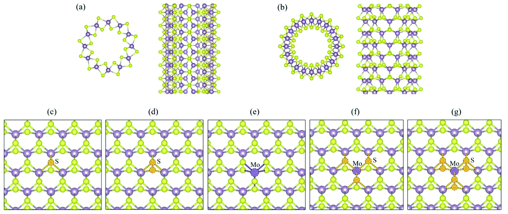 | ||
| Fig. 1 (a) Top view and side view of a (6, 6) tube; (b) top view and side view of a (10, 0) tube. Topologies of (c) VS, (d) VS2, (e) VMo, (f) VMoS3, and (g) VMoS6 vacancies. The removed atoms are highlighted as dashed-line balls. | ||
3.1 MoS2 tube with VS defect
We begin our analysis with a (6, 6) tube with a VS defect. The presence of a significant number of S vacancies in MoS2 was directly observed by high-resolution TEM.18,19,22 In our calculations, the VS vacancy has a formation energy of 2.31 eV for the (6, 6) tube and a comparable value of 2.35 eV for the (10, 0) tube. These values are higher than that for the MoS2 monolayer (1.56 eV) and than those obtained in an earlier computational study.36 The higher formation energy of the defect can be attributed to the curvature of the tube wall. In Fig. 2a and b, we show the plots of the band structures of defect-free and defect-laden (6, 6) tube for comparison. It is found that the (6, 6) tube with VS remains semiconducting with an indirect bandgap. In addition, the spin-up and spin-down branches are totally degenerated, indicating that the system is nonmagnetic. The bandgap slightly decreases from 0.25 to 0.24 eV. Another significant change is that the valence band (VB) and conduction band (CB) become flat, as shown in Fig. 2b. The flat band usually represents a spatially localized electron state in real space, corresponding to carriers with large effective masses. To quantitatively assess the regulation of defects to charge carriers, we calculated the effective mass by m* = ℏ2[∂2E(k)/∂k2]−1 at the valence band maximum (VBM, the hole) and conductance band minimum (CBM, the electron). The m* value of a hole is −2.16me, which is larger than that of the defect-free (6, 6) tube (only −0.83me).17 The m* value of an electron is 1.16me, which is also larger than that of the defect-free (6, 6) tube (only 0.53me).17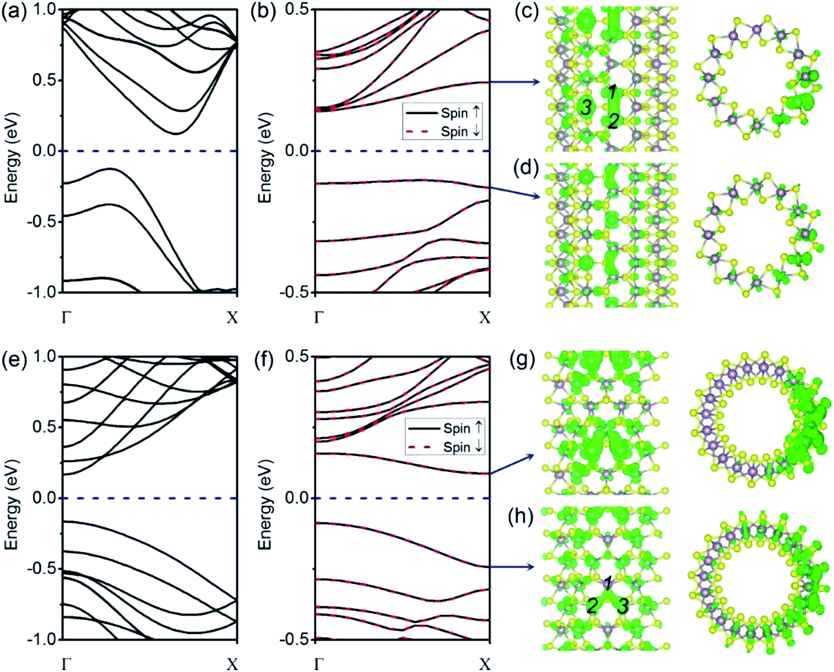 | ||
| Fig. 2 Band structures of (a) pristine (6, 6) tube and (b) (6, 6) tube with VS vacancy. Electron isosurfaces of (c) CB and (d) VB. Band structures of (e) pristine (10, 0) tube and (f) (10, 0) tube with VS vacancy. Electron isosurfaces of (g) CB and (h) VB. The isosurface cutoff is 0.001|e|/Å3. | ||
The isosurfaces of the electron states of the CB and VB are shown in Fig. 2c and d, respectively. Evidently, the CB and VB represent the unsaturated states at Mo atoms around the S vacancy. In addition, it is also found that the electron clouds between Mo 1–2 overlap along the tube's axial direction. In contrast, the cloud at Mo 3 is isolated. First, this should be mainly attributed to the small distance between Mo 1–2 (3.20 Å) as compared to the distance of 3.59 Å for Mo 1–3 or Mo 2–3. In addition, this phenomenon may refer to the fact that an electron coupling is stronger along the zigzag direction (axial direction of the tube) than that along the armchair direction.
For the case of a pristine (10, 0) tube, it is a direct-bandgap semiconductor: both the VBM and CBM are located at the Γ (0, 0, 0) point, as shown in Fig. 2e. However, when one VS is introduced, the bandgap becomes indirect: the CBM moves to the χ (0, 0, 0.5) point (Fig. 2f). The VS defect also suppresses the gap, from 0.33 eV for an ideal tube to 0.17 eV for a defect-laden tube. The spin-up and spin-down branches are totally degenerated, indicating no polarization. In Fig. 2g and h, we show the plots of the isosurfaces of the electron states of the VB and CB. It is clear that the VB and CB mainly spread around the Mo-edge atoms near the missing S. The electron clouds are dispersed within Mo 1–2 and Mo 1–3. In contrast, no electron cloud is found in Mo 2–3. We mainly attribute this electron cloud pattern to the different distances between the three Mo atoms. In detail, the distance between Mo 1–2 and Mo 1–3 is 3.24 Å; however, for Mo 2–3, this distance is larger, namely, 3.62 Å. Another feature is that the introduction of the VS defect changes the m* values of the hole and electron in an opposite trend. In detail, the m* value of the hole is −1.37me, which is smaller than that of the defect-free (10, 0) tube (−1.55me). On the contrary, the m* value of the electron is 1.68me, which is significantly larger than that of the defect-free (10, 0) tube (only 0.51me).17
3.2 MoS2 tube with VS2 defect
As compared to the VS defect, our results reveal that the VS2 defect induces dramatic changes in the (6, 6) tube. Firstly, the formation energy for a VS2 defect is relatively high, 5.07 eV for the (6, 6) tube and 5.03 eV for the (10, 0) tube. The high formation energy indicates that the removal of disulfur atoms, resulting in three Mo-edge atoms, is difficult. This is consistent with earlier studies in which it was shown that Mo-terminated edges in MoS2 are highly unstable.33 From the band structures (Fig. 3a), it is evident that the first change involves the (6, 6) tube bearing a VS2 defect becoming metallic. It is noteworthy that only one band of a spin-down channel crosses the Fermi level. However, the spin-up channel has an indirect bandgap of 0.16 eV. Therefore, the tube is half-metallic: it only allows spin-down transport while blocking spin-up transport. This property reveals the prospective applications of (6, 6) tubes in the design of spintronic devices via defect engineering. Secondly, the system is spin-polarized with net magnetic moment of 1.75 μB. To reveal the origin of spin polarization, the atomic- and orbital-projected electron densities of states (PDOS) were analyzed, and these results are shown in Fig. 3b and c. The net spin was found to be mainly contributed by Mo atoms, with only minor contributions from S atoms. In addition, the spin polarization mainly happened for the d-orbital electrons of Mo. In addition, the isosurface of net spin (magnetic moment) is shown in Fig. 3d. The shape of the net spin is mainly located on Mo 1 and Mo 2 and has a character of dx2−y2/dxy hybrid orbitals. This is consistent with the above PDOS analyses. For a MoS2 monolayer, the dx2−y2 and dxy orbitals contribute to the Mo–S bonds becoming energy-degenerated.17 The net spin near the VS2 defect is mainly contributed by the unsaturated electrons because of the missing S atoms. In addition, among the three Mo atoms at the defect edge, the spin mainly spreads around Mo 1 and Mo 2, which aligns along the tube's axial direction (namely, the zigzag direction). Hence, the spin coupling in MoS2 NTs is similar to the case of graphene ribbons, where a ferromagnetic coupling can only form in the zigzag-edged graphene ribbons. While for armchair ribbons, the coupling between adjacent spins are weak.37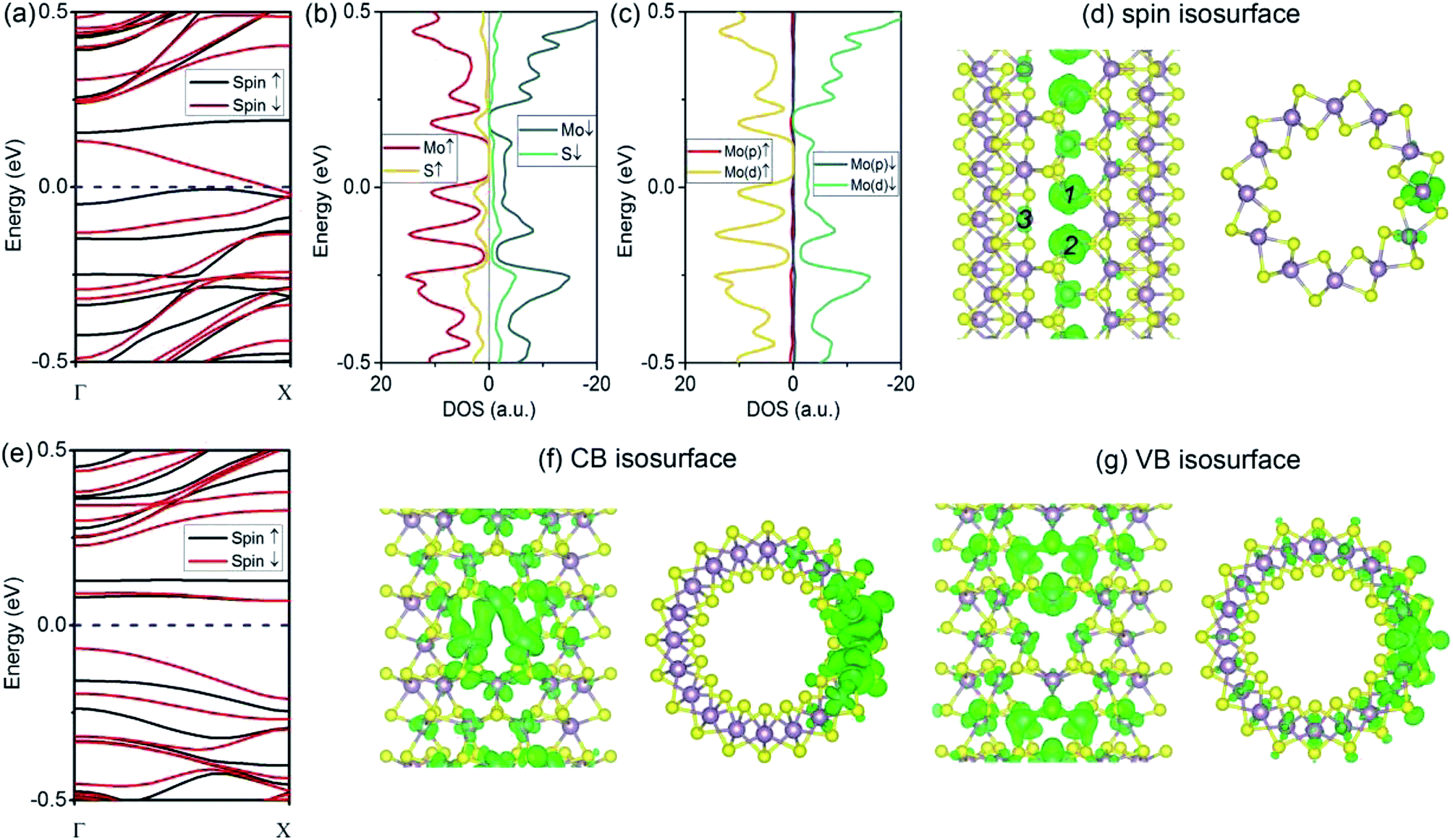 | ||
| Fig. 3 (a) Band structures of a (6, 6) tube with a VS2 defect; (b) atomic-projected DOS; (c) Mo-orbital-projected DOS; (d) spin isosurface (cutoff = 0.003|e|/Å3); (e) band structures of a (10, 0) tube with a VS2 defect; (f and g) charge isosurfaces of CB and VB (cutoff = 0.001|e|/Å3). | ||
In contrast to the (6, 6) tube (which becomes half-metallic upon the introduction of a VS2 defect), the (10, 0) tube remains semiconducting. However, the gap becomes indirect because the VBM is located at the Γ point, while the CBM moves to the X point (Fig. 3e). In addition, all the branches of the bands are polarized, although the net spin is zero. Such a spin-polarized band structure exhibits two distinct energy gaps for the two spin components: the gap is 0.23 eV for spin-up, while it is only 0.14 eV for spin-down. In addition, the CB is considerably flat, indicating that the electron carriers are highly localized at the defect site (Fig. 3f) with considerably large m*. Our results indicate that for electron carriers, the values of m* are 5.99me (spin-up) and 4.47me (spin-down). These values are considerably larger than that of an ideal (10, 0) tube (0.51me). Hence, the CB is better recognized as an “impurity state.” Similarly, the VB of spin-up is also considerably flat at the VBM, resulting in large m* values for holes (−4.65me) (as compared to −1.55me for an ideal tube). In Fig. 3f and g, we show the plots of the isosurfaces corresponding to the VB and CB. It is clear that the electron states are localized. The only exception is that the VB of spin-down is more dispersed in energy, representing holes of −1.32me.
3.3 MoS2 tube with VMo defect
The introduction of a VMo defect corresponds to the formation energy of 2.25 eV for (6, 6) tubes and 1.89 eV for (10, 0) tubes. This value is comparable to that of a VS vacancy. The removal of a single Mo atom leaves S-edge atoms, which are predicted to be stable from an earlier study.33 The VMo defect also induced significant changes to the (6, 6) tube. As depicted by the spin-polarized band structures (Fig. 4a), the system becomes metallic, with one band representing spin-up and one band representing spin-down crossing the Fermi level. Therefore, in contrast to the (6, 6) tube bearing a VS2 defect, the tube with the VMo defect has no spin selectivity. As the electron occupations are different for the two spin components, the system has a net magnetic moment of 1.10 μB, which is smaller than that of VS2. From the PDOS analyses (Fig. 4b and c), the net spin was mainly attributed to the d-orbital electrons from the Mo atoms. This phenomenon is consistent with the case of (6, 6) tubes with VS2 defects. The spin isosurface is shown in Fig. 4d, from which it is evident that spin polarization takes place not at the bare S atoms at the VMo edge, but mainly at the Mo atoms around the defect. | ||
| Fig. 4 (a) Band structures of a (6, 6) tube with a VMo defect; (b) atomic-projected DOS; (c) Mo-orbital-projected DOS; (d) spin isosurface (cutoff = 0.001|e|/Å3); (e) band structures of a (10, 0) tube with a VMo defect; (f and g) charge isosurfaces of two bands at the Fermi level (cutoff = 0.001|e|/Å3). | ||
Finally, we assess the effects of VMo defects on (10, 0) tubes. From the band structures shown in Fig. 4e, it is clear that all the bands that represent spin-up and spin-down are degenerated; therefore, the system is nonpolarized. This is similar to the cases of the (6, 6) and (10, 0) tubes with VS defects. The most significant change is that there are two bands at the Fermi level, contributing to metallic conductivity. From the isosurfaces of the electron states representing these two bands (Fig. 4f and g), it can be seen that the conducting states are mainly contributed by the Mo atoms that are spread along the tube's axial direction.
3.4 MoS2 tube with VMoS3 defect
Next, we consider the vacancy type with a relatively large size, i.e., VMoS3. From our calculations, the introduction of a VMoS3 vacancy requires a formation energy of 5.21 eV for the (6, 6) tube and 5.33 eV for the (10, 0) tube. These values are comparable to that of the VS2 vacancy in MoS2 tubes, as discussed above. In fact, the two species of defects, VS2 and VMoS3, have been directly observed experimentally in the MoS2 monolayer. Therefore, they can exist in the MoS2 tube. For the electronic properties, we firstly considered the case of the (6, 6) tube. From the band structures shown in Fig. 5a, it is evident that the first change involves the (6, 6) tube bearing VMoS3 becoming metallic. In addition, similar to the case of the (6, 6) tube with VS2 (which is conducting only for spin-down), the bands representing the spin-down channel cross the Fermi level. However, the bandgap for the spin-up bands is 0.12 eV. Therefore, the (6, 6) tube with VMoS3 is conducting for the spin-down channel, while the spin-up channel is blocked. This phenomenon is similar to the case of the (6, 6) tube with a VS2 defect. As the bands near the Fermi level are severely modulated by the VMoS3 defect, the net magnetic moment of each vacancy is as large as 4 μB. From the PDOS analyses shown in Fig. 5b and c, it is clear that the net spin was mainly contributed by the d-orbital electrons from the Mo atoms. Spatially, the net spin is located at the Mo atoms near the vacancy edge, as shown in Fig. 5d. | ||
| Fig. 5 (a) Band structures of a (6, 6) tube with a VMoS3 defect; (b) atomic-projected DOS; (c) Mo-orbital-projected DOS; (d) spin isosurface (cutoff = 0.003|e|/Å3); (e) band structures of a (10, 0) tube with a VMoS3 defect; (f) atomic-projected DOS; (g) Mo-orbital-projected DOS; (h) spin isosurface (cutoff = 0.003|e|/Å3). | ||
For the (10, 0) tube, it is still semiconducting, which is similar to the case of a pristine (10, 0) tube. As shown in Fig. 5e, there are still worthwhile spintronics that may exist for the (10, 0) tube. In detail, it is a direct-bandgap semiconductor for the spin-down channel, while it is indirect for the spin-up channel. Secondly, the system is also spin-polarized with integer net magnetic moment of 2 μB. From the PDOS analyses shown in Fig. 5f and g, the net spin was mainly attributed to the d-orbital electrons from the Mo atoms. From the spatial distributions shown in Fig. 5h, it is clear that all of them are localized at the Mo atoms even if the S atoms at the vacancy edges have dangling bonds. By comparing the spin distributions in the (6, 6) tube with those in the (10, 0) tube, it is found that the net spins on the Mo atoms arranged along the zigzag direction (the (6, 6) tube's axial direction) can form a strong ferromagnetic coupling, as shown in Fig. 5d, which is absent in the case of the (10, 0) tube (Fig. 5h).
3.5 MoS2 tube with VMoS6 defect
Finally, we analyze the VMoS6 defect, which has the largest size. Initially, we analyzed the formation of such a defect. From our calculations, the formation energy of a VMoS6 defect is rather high: 17.31 eV for the (6, 6) tube and 16.63 eV for the (10, 0) tube. For comparison, the corresponding value in a MoS2 monolayer is estimated to be 11.0 eV.36 Although the formation energy is high, such a vacancy is still found in the experiment,18 but the concentration might be low. For the (6, 6) tube with a VMoS6 defect, the band structure (Fig. 6a) indicates that it is semiconducting. The two spin branches near the Fermi level are rather flat, indicating spatially localized states. Among all the situations in the present study, the VMoS6 defect in the (6, 6) tube induces the most significant spin polarization with net magnetic moment of 6 μB. From the atomic- and orbital-projected DOS data (Fig. 6b and c), the net spin is mainly attributed to the d-orbital of Mo atoms, which is similar to the other spin-polarized states in the aforementioned systems. The spin isosurface shown in Fig. 6d also points to the fact that the spins are highly localized at the Mo atoms at the defect edge. By labeling the four atoms in Fig. 6d that bear a net spin (atom 4 is antiferromagnetically coupled), it is also worth noticing that the adjacent spins can form a strong coupling along the zigzag direction (tube's axis). In contrast, the (10, 0) tube with a VMoS6 defect is nonmagnetic, although it is also rich in Mo-edge atoms (Fig. 6e). The CB and VB are relatively flat, representing the local states, as demonstrated in Fig. 6f and g. From the abovementioned results, it is evident that spin polarization in the (10, 0) tube can only happen by introducing VMoS3 defects.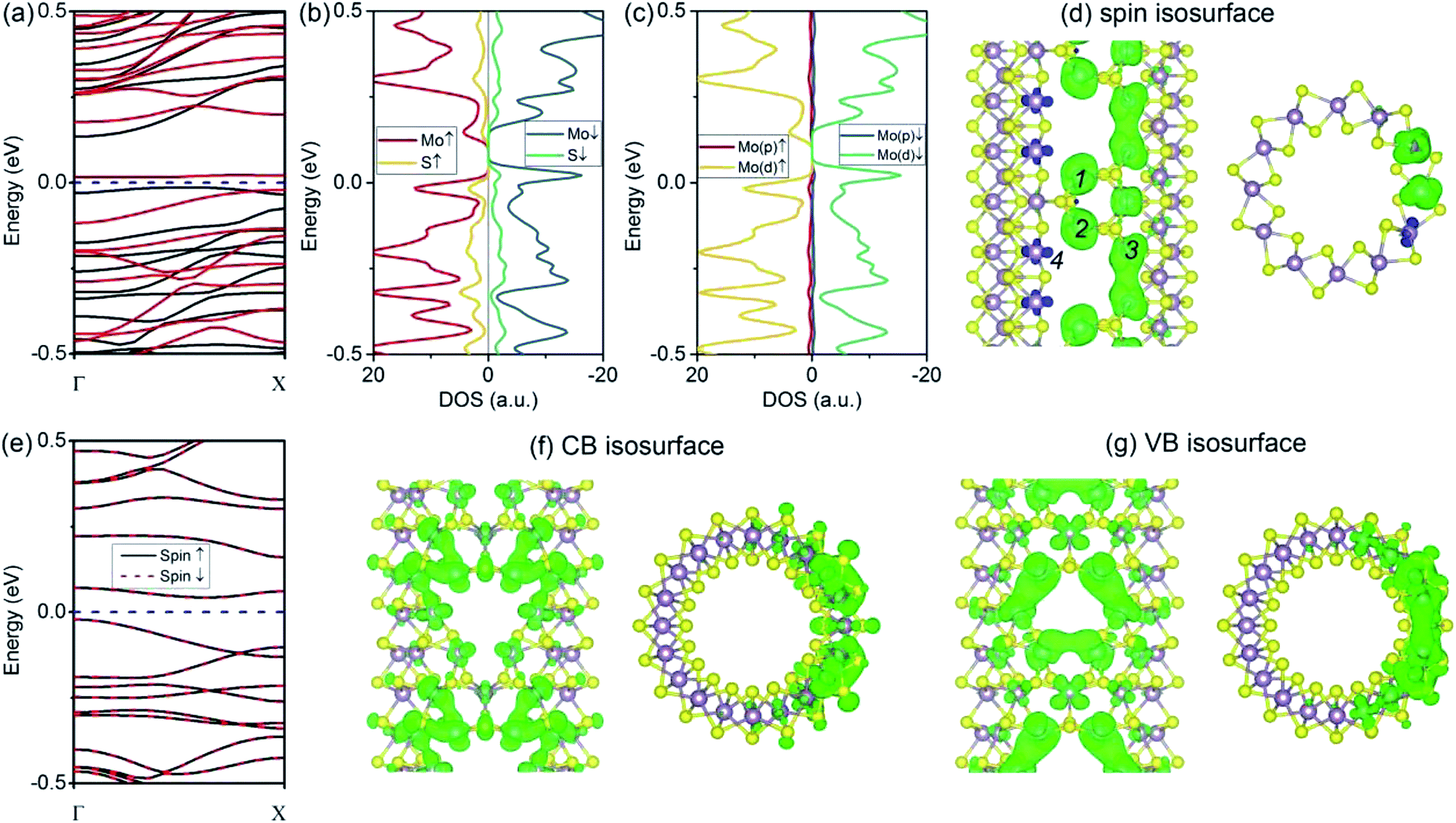 | ||
| Fig. 6 (a) Band structures of a (6, 6) tube with a VMoS6 defect; (b) atomic-projected DOS; (c) Mo-orbital-projected DOS; (d) spin isosurface (cutoff = 0.005|e|/Å3); (e) band structures of a (10, 0) tube with a VMoS6 defect; (f and g) charge isosurfaces of the CB and VB (cutoff = 0.002|e|/Å3). | ||
4. Conclusions
To summarize, we have systematically investigated the electronic and magnetic properties of MoS2 NTs with vacancy defects. We found that the (6, 6) tube with VS2/VMo/VMoS3 defects and the (10, 0) tube with VMo vacancy become metallic. It is interesting that the (6, 6) tube with VS2/VMoS3 vacancies has a half-metallic character, which only allows the transport of electrons with only one spin direction, but exhibits an indirect bandgap of 0.16 eV for the opposite spin direction. In contrast, the (6, 6) tube with VS/VMoS6 defects and (10, 0) tube with VS/VS2/VMoS3/VMoS6 defects remain semiconducting. With regard to the magnetic properties, it is found that the (6, 6) tube with VS2/VMo/VMoS3/VMoS6 defects can bear net magnetic moment. For the (10, 0) tube, magnetization was only observed for VMoS3 defects. Therefore, our results demonstrate that defect engineering is an effective way to control the electronic and magnetic properties of MoS2 NTs. By controlling the types of vacancies, metallic and half-metallic conductivities can be realized. We hope that our present findings can stimulate related experimental studies in these areas and assist formulating the ultimate functions of MoS2 materials for future nanoelectronic and spintronic devices.Conflicts of interest
There are no conflicts to declare.Acknowledgements
This work is supported by Shandong Provincial Natural Science Foundation, China (No. ZR2018MA034) and the National Natural Science Foundation of China (No. 11874238). The authors thank the National Super Computing Centre in Jinan for providing computing facilities.References
- J. N. Coleman, M. Lotya, A. O'Neill, S. D. Bergin, P. J. King, U. Khan, K. Young, A. Gaucher, S. De and R. J. Smith, Science, 2011, 331, 568–571 CrossRef CAS PubMed.
- B. Radisavljevic, A. Radenovic, J. Brivio, V. Giacometti and A. Kis, Nat. Nanotechnol., 2011, 6, 147–150 CrossRef CAS PubMed.
- B. Radisavljevic, M. B. Whitwick and A. Kis, ACS Nano, 2011, 5, 9934–9938 CrossRef CAS PubMed.
- D. J. Late, B. Liu, H. S. S. R. Matte, V. P. Dravid and C. N. R. Rao, ACS Nano, 2012, 6, 5635–5641 CrossRef CAS PubMed.
- M. Shanmugam, T. Bansal, C. A. Durcan and B. Yu, Appl. Phys. Lett., 2012, 100, 153901 CrossRef.
- C. Ataca and S. Ciraci, Phys. Rev. B: Condens. Matter Mater. Phys., 2012, 85, 195410 CrossRef.
- Y. Li, H. Wang, L. Xie, Y. Liang, G. Hong and H. Dai, J. Am. Chem. Soc., 2011, 133, 7296–7299 CrossRef CAS PubMed.
- T. F. Jaramillo, K. P. Jørgensen, J. Bonde, J. H. Nielsen, S. Horch and I. Chorkendorff, Science, 2007, 317, 100–102 CrossRef CAS PubMed.
- L. Wang, Y. Wang, J. I. Wong, T. Palacios, J. Kong and H. Y. Yang, Small, 2014, 10, 1101–1105 CrossRef CAS PubMed.
- C. Zhu, Z. Zeng, H. Li, F. Li, C. Fan and H. Zhang, J. Am. Chem. Soc., 2013, 135, 5998–6001 CrossRef CAS PubMed.
- S. Wang, K. Li, Y. Chen, H. Chen, M. Ma, J. Feng, Q. Zhao and J. Shi, Biomaterials, 2015, 39, 206–217 CrossRef CAS PubMed.
- A. Kis, D. Mihailovic, M. Remskar, A. Mrzel, A. Jesih, I. Piwonski, A. J. Kulik, W. Benoît and L. Forró, Adv. Mater., 2003, 15, 733–736 CrossRef CAS.
- M. Remskar, A. Mrzel, Z. Skraba, A. Jesih, M. Ceh, J. Demšar, P. Stadelmann, F. Lévy and D. Mihailovic, Science, 2001, 292, 479–481 CrossRef CAS PubMed.
- M. Remskar, A. Mrzel, M. Virsek, M. Godec, M. Krause, A. Kolitsch, A. Singh and A. Seabaugh, Nanoscale Res. Lett., 2011, 6, 26 Search PubMed.
- G. Seifert, H. Terrones, M. Terrones, G. Jungnickel and T. Frauenheim, Phys. Rev. Lett., 2000, 85, 146 CrossRef CAS PubMed.
- L. Xu, PhD Dissertation, Clemson University, Clemson, S. C., USA, 2007.
- W. Li, G. Zhang, M. Guo and Y.-W. Zhang, Nano Res., 2014, 7, 1–10 CrossRef.
- W. Zhou, X. Zou, S. Najmaei, Z. Liu, Y. Shi, J. Kong, J. Lou, P. M. Ajayan, B. I. Yakobson and J.-C. Idrobo, Nano Lett., 2013, 13, 2615–2622 CrossRef CAS PubMed.
- H. Qiu, T. Xu, Z. Wang, W. Ren, H. Nan, Z. Ni, Q. Chen, S. Yuan, F. Miao and F. Song, Nat. Commun., 2013, 4, 2642 CrossRef PubMed.
- Z. Yu, Y. Pan, Y. Shen, Z. Wang, Z. Y. Ong, T. Xu, R. Xin, L. Pan, B. Wang and L. Sun, Nat. Commun., 2014, 5, 5290 CrossRef CAS PubMed.
- J. Hong, Z. Hu, M. Probert, K. Li, D. Lv, X. Yang, L. Gu, N. Mao, Q. Feng and L. Xie, Nat. Commun., 2015, 6, 6293 CrossRef CAS PubMed.
- H.-P. Komsa, J. Kotakoski, S. Kurasch, O. Lehtinen, U. Kaiser and A. V. Krasheninnikov, Phys. Rev. Lett., 2012, 109, 035503 CrossRef PubMed.
- K. C. Santosh, C. L. Roberto, A. Rafik, M. W. Robert and C. Kyeongjae, Nanotechnology, 2014, 25, 375703 CrossRef PubMed.
- Y. Ouyang, C. Ling, Q. Chen, Z. Wang, L. Shi and J. Wang, Chem. Mater., 2016, 28, 4390–4396 CrossRef CAS.
- J. Xie, H. Zhang, S. Li, R. Wang, X. Sun, M. Zhou, J. Zhou, X. W. Lou and Y. Xie, Adv. Mater., 2013, 25, 5807–5813 CrossRef CAS PubMed.
- G. Ye, Y. Gong, J. Lin, B. Li, Y. He, S. T. Pantelides, W. Zhou, R. Vajtai and P. M. Ajayan, Nano Lett., 2016, 16, 1097–1103 CrossRef CAS PubMed.
- H. Nan, Z. Wang, W. Wang, Z. Liang, Y. Lu, Q. Chen, D. He, P. Tan, F. Miao, X. Wang, J. Wang and Z. Ni, ACS Nano, 2014, 8, 5738–5745 CrossRef CAS PubMed.
- F. Fabbri, E. Rotunno, E. Cinquanta, D. Campi, E. Bonnini, D. Kaplan, L. Lazzarini, M. Bernasconi, C. Ferrari, M. Longo, G. Nicotra, A. Molle, V. Swaminathan and G. Salviati, Nat. Commun., 2016, 7, 13044 CrossRef CAS PubMed.
- G. Kresse and J. Furthmuller, Comput. Mater. Sci., 1996, 6, 15–50 CrossRef CAS.
- G. Kresse and J. Furthmuller, Phys. Rev. B: Condens. Matter Mater. Phys., 1996, 54, 11169–11186 CrossRef CAS.
- P. E. Blochl, Phys. Rev. B: Condens. Matter Mater. Phys., 1994, 50, 17953–17979 CrossRef.
- J. P. Perdew, J. A. Chevary, S. H. Vosko, K. A. Jackson, M. R. Pederson, D. J. Singh and C. Fiolhais, Phys. Rev. B: Condens. Matter Mater. Phys., 1992, 46, 6671–6687 CrossRef CAS.
- H. Pan and Y.-W. Zhang, J. Mater. Chem., 2012, 22, 7280–7290 RSC.
- S. B. Zhang, J. Phys.: Condens. Matter, 2002, 14, R881–R903 CrossRef CAS.
- H. Pan, Y.-W. Zhang, V. Shenoy and H. Gao, Appl. Phys. Lett., 2010, 96, 192510 CrossRef.
- H.-P. Komsa and A. V. Krasheninnikov, Phys. Rev. B: Condens. Matter Mater. Phys., 2015, 91, 125304 CrossRef.
- Y.-W. Son, M. L. Cohen and S. G. Louie, Phys. Rev. Lett., 2006, 97, 216803 CrossRef PubMed.
| This journal is © The Royal Society of Chemistry 2019 |