
 Open Access Article
 This Open Access Article is licensed under a Creative Commons Attribution-Non Commercial 3.0 Unported Licence
A straightforward chemical approach for excellent In2S3 electron transport layer for high-efficiency perovskite solar cells†
Fengyang Yua,
Wangen Zhao*a and
Shengzhong (Frank) Liu *ab
*ab
aKey Laboratory of Applied Surface and Colloid Chemistry, National Ministry of Education, Shaanxi Engineering Lab for Advanced Energy Technology, School of Materials Science and Engineering, Shaanxi Normal University, Xi'an 710062, China. E-mail: wgzhao@snnu.edu.cn
bDalian Institute of Chemical Physics, Dalian National Laboratory for Clean Energy, Chinese Academy of Sciences, Dalian, 116023, China
First published on 8th January 2019
Abstract
Perovskite solar cells (PSCs) have attracted significant attention in recent years owing to some of their advantages: high-efficiency, low cost and ease of fabrication. In perovskite photovoltaic devices, charge transport layers play a vital role for selectively extracting and transporting photo-generated electrons and holes to opposite electrodes. Therefore, it is very important to prepare high-quality charge transport layers using simple processes at low cost. As reported, In2S-based electron selective layers display excellent performance including high solar-cell efficiency and negligible hysteresis. In this study, a simple chemical method was developed to prepare In2S3 thin films as the electron selective layers in organic–inorganic hybrid perovskite photovoltaic devices to shorten the fabrication time and simplify the technology, which can provide a new avenue for a low-cost and solution-processed method. By optimizing the preparation conditions, it was demonstrated that In2S3 thin film prepared using our straightforward chemical approach have higher electron extraction efficiency and comparable efficiency compared with archetypical TiO2 as the electron transport layer (ETL) in perovskite photovoltaic device.
Introduction
Halide perovskites undoubtedly represent one of the most prospective photovoltaic semiconductors for light-absorbing materials due to some of their appealing optoelectronic attributes; this has contributed to unbelievable achievements in power-conversion efficiency (PCE) beyond 20% just in a few years,1–7 matching with and even surpassing those of the state-of-the-art CdTe and monocrystalline silicon solar cells. Up to now, PCE of PSCs has been as high as about 23.3%,8 and the value keeps persistently improving. Generally, the classic PSC photovoltaic devices are designed using a “sandwich” architecture, in which the light-harvesting layer lies between efficient ETL and hole transporting layer (HTL). Regular n–i–p and inverted p–i–n are the two types of planar structures on account of the sequence of the charge transport layers.9–15 Therefore, in the pursuit of advancement or improvement in the performance or fabrication cost, many attempts have been made to optimize the absorption layer, electron transport layer,16–19 hole transport layer,20–28 and the interfaces between the adjacent layers.29,30 Until now, compact TiO2 layers are the most widely utilized inorganic ETLs. However, the application of TiO2 ETL in PSCs is limited due to its high-temperature fabrication and intrinsic low carrier mobility.31–33 Hence, some research communities have been investigating alternative ETL materials, including some organics (PCBM (6,6)-phenyl-C61-butyric acid methyl ester,34–36 C60,37,38 and N,N′-bis(3-(dimethylamino)propyl)-5,11-dioctylcoronene-2,3,8,9-tetracarboxdiimide (CDIN))39 and widely employed inorganic semiconductor materials such as ZnO,18,40 SnO2,41–44 WOx,45 In2O3,46 CdS,32,47,48 Fe2O3,49 Zn2SnO4,50–52 and Nb2O5.53 Recently, Yang's group found that well-organized In2S3 nanoflake arrays can be applied in perovskite solar cells as the ETL with better performance (higher efficiency and less hysteresis) compared to commonly used TiO2-based solar cells.54 The In2S3 thin film exhibited superior performance compared to TiO2 owing to its higher carrier mobility (17.6 cm2 V−1 s−1 vs. 10−4 cm2 V−1 s−1). However, the In2S3 thin film deposition is a complicated chemical bath process that requires several hours, which is time-consuming and energy-intensive.In this scenario, we fabricated In2S3 thin films using a simple method that shortened the process time to several minutes. By optimizing the concentration of the metal precursors and deposition parameters, a smooth In2S3 film was obtained. In fact, In2S3 ETL performed better than the most commonly used TiO2 in extracting and transporting electrons. Moreover, the photovoltaic devices utilizing the In2S3 thin films as the ETL exhibited PCE of 15.48%.
Results and discussion
Fig. 1 shows a schematic for the preparation of In2S3 thin film and the PSC device assembly. The In2S3 thin film was prepared by dissolving In(OH)3 in butyldithiocarbamic acid, which was formed via a reaction between carbon disulfide and butylamine in situ in ethanol at room temperature, followed by annealing. To decide a suitable sintering temperature for depositing the compact In2S3 thin film, the thermal decomposition behaviour of In-complex was studied by thermogravimetric (TG) analysis exhibited in Fig. S1.† Before the TG measurement, In-complex solution with high concentration was dried at 40 °C for a couple of days to remove the solvents and excess ligands. The acquired solid In-complex precursor was studied in the temperature range of 100–500 °C in nitrogen atmosphere. From the TG curve, it is clear that there is no further loss when the temperature increased up to 225 °C, suggesting the annealing temperature to prepare In2S3 thin films. Therefore, we determined that the In2S3 thin film could be sintered at 200 °C for 1 min to remove organic ligands and solvents and subsequently at 300 °C for 2 min to further burn off the leftovers to obtain the In2S3 thin film.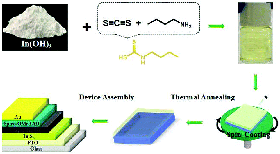 | ||
| Fig. 1 The schematic of the synthesis of In2S3 film and device assembly. | ||
For identifying the In2S3 thin film, the valence states of In and S ions in the annealed thin film were researched, as shown in Fig. S2.† It can be seen that In 3d peaks are located at 444.4 eV and 452 eV with a splitting value of 7.6 eV, and S 2p peaks are located at 160.8 eV and 162.4 eV with a splitting value of 1.6 eV, which are associated with In3+ and S2− ions, respectively.55 In addition, EDS (energy dispersive spectroscopy) analysis was also conducted to check the ratios of In and S in the prepared thin film (Fig. S3†). The results revealed that the thin film exhibited the ratio of S![[thin space (1/6-em)]](https://www.rsc.org/images/entities/char_2009.gif) :In = 11.6:7.8, which is accurately consistent with 3:2, corresponding to the stoichiometric ratio. Subsequently, the device was assembled in a typical structure with Spiro-OMeTAD as the hole transport layer; also, Au and FTO were employed as the electrodes, and organic–inorganic hybrid perovskite was used as the absorbing material.
:In = 11.6:7.8, which is accurately consistent with 3:2, corresponding to the stoichiometric ratio. Subsequently, the device was assembled in a typical structure with Spiro-OMeTAD as the hole transport layer; also, Au and FTO were employed as the electrodes, and organic–inorganic hybrid perovskite was used as the absorbing material.
The relative valence band and conductive band positions of ETL, absorbing layer and HTL affect the routes for the electron and hole transport, which is the core for designing the battery architecture. Thus, the valence band maximum (VBM) and Fermi energy of the In2S3 thin film were investigated by UPS (ultraviolet photoelectron spectroscopy) (Fig. S4†). The Fermi energy was first obtained as −3.86 eV by subtracting the spectrum onset of 17.36 eV from the ultraviolet photoelectron energy of 21.22 eV.32 By linear extrapolation in the low binding energy region, the distance between Fermi energy and VBM was calculated as 2.23 eV. Thus, the value of VBM is −6.09 eV. The optical band gap of In2S3 was calculated from ultraviolet-visible absorption spectra and Tauc formula to be 2.29 eV. Thus, the conduction band energy (Ec) was calculated to be −3.8 eV, according to the equation Ec = VBM + Eg. The valence band and conduction band values of other layers were obtained from the literature.46 The relative energy-level diagram of the PSC device is shown in Fig. 2(a). We found that In2S3 has a suitable energy level to promote the extraction of electrons. The conduction band minimum (CBM) of CH3NH3PbI3 is closer to that of In2S3 than to that of TiO2, which leads to lower energy barrier for electron injection from the perovskite layer into In2S3 ETL. Fig. 2(b) shows the transmittance spectra for In2S3 coated on FTO/glass substrates with different In precursor concentrations. The transmittance of In2S3 thin film decreased with increase in the precursor concentration. Especially, the transmittance of In2S3 film sharply decreased in the 300–500 nm range, which was due to its narrow band gap. The thicker the In2S3 thin film, the stronger the absorbance. The absorbance of In2S3 thin film can result in decrease in light for the perovskite absorber layer, which was presented by Jsc of the solar cell. The image of In2S3 thin film deposited on different concentrations is displayed in Fig. 2(c), in which it can be clearly seen that the In2S3 thin film gradually turned more yellow with increase in the precursor concentration, illustrating that a thicker In2S3 thin film was deposited.
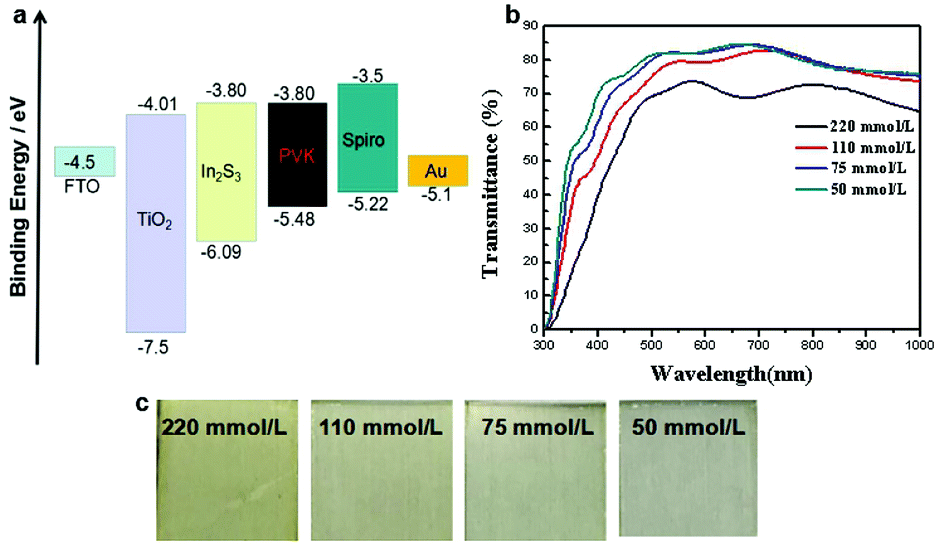 | ||
| Fig. 2 (a) The energy-level diagram of the PSC device and (b) the transmittance spectra of In2S3 thin films with different In concentrations; (c) the photograph of In2S3 thin film deposited on different concentrations. | ||
Atomic force microscopy (AFM) measurements were obtained to characterize the surface properties of In2S3 thin films (Fig. S5†). The flatness of the In2S3 film was approximate to that of TiO2, and it was even more smoother. Smooth substrates are beneficial for the formation of even perovskite layers. The top-view SEM images of the prepared In2S3 films on FTO substrates with different precursor concentrations are shown in Fig. 3(a)–(d), which demonstrate a great change in the film morphology. With decrease in the concentration of In precursor, the amount of pinholes in the films decreased except for 50 mmol L−1 concentration due to possible incomplete coverage. It can be explained that more small organic ligands escape from the film during the heating process when the concentration of the precursor is high. Therefore, seeking In2S3 with suitable In concentration and thickness is important for application in PSCs.
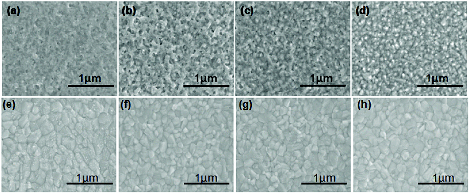 | ||
| Fig. 3 Top-view SEM (scanning electron microscopy) images of In2S3 films on FTO substrates and perovskite films coated on relative In2S3 ETLs with different precursor concentrations of (a) and (e) 220 mmol L−1, (b) and (f) 110 mmol L−1, (c) and (g) 75 mmol L−1, (d) and (h) 50 mmol L−1. | ||
CH3NH3PbI3 absorption layers were coated on In2S3 ETLs using a typical one-step solution process; the corresponding SEM images are exhibited in Fig. 3(e)–(h). The quality of the perovskite films was influenced by In2S3 substrates. All the perovskite films were compact and uniform except for the perovskite layer coated on In2S3 thin film with 220 mmol L−1 precursor, which exhibited some small granules on the perovskite surface. The appearance of the small granules may be due to incomplete decomposition of the In2S3 film. A high concentration resulted in thick thin film, which needed longer time to decompose In-complex. Thus, small organic molecules escaped from the In2S3 film during the subsequent annealing process to prepare the perovskite layer. It can be seen that the pinholes in the In2S3 films have different sizes and depths, where deeper/larger pinholes have more serious impact on the quality of the films. Fig. S6† shows the AFM height images of the CH3NH3PbI3 films based on different In2S3 films. It is clear that all the films are flat, and the RMS values of all the perovskite films are less than 10 nm. Smooth absorption layers provide high-quality surfaces for electron transport, which are necessary for high-efficiency devices.
In addition, the ultraviolet-visible-near infrared (UV-vis-NIR) absorption spectra, room-temperature photoluminescence (PL) spectra and external quantum efficiency (EQE) for the perovskite films or solar cells based on different In precursor concentrations were measured. As demonstrated in Fig. 4(a), the absorbance intensity of perovskite films coated on In2S3 ETLs enhanced with the increase of In2S3 film thickness, especially in the 300–500 nm range, which is in agreement with the transmittance of In2S3 films due to the absorbance of In2S3 thin film. The PL spectra shown in Fig. 4(b) reveal the presence of weak photoluminescence of CH3NH3PbI3 samples based on different In2S3 thin films, which indicates the low level of recombination of electron–hole pairs because the photo-generated electrons are transferred quickly to ETL. In particular, the sample with 75 mmol L−1 precursor concentration exhibited the lowest intensity, indicating that 75 mmol L−1 is the suitable concentration for fabricating perovskite solar cells. The current density–voltage (J–V) characteristics for PSCs with In2S3 ETLs with different concentrations were measured under simulated AM 1.5 G solar irradiation, as shown in Fig. 4(c). The values of short-circuit current density (Jsc), open-circuit voltage (Voc), fill factor (FF) and power-conversion efficiency (η) were obtained from the J–V curves, as summarized in Table S1.† Evidently, PSCs with In2S3 ETL prepared with the concentration of 75 mmol L−1 exhibited Jsc, Voc and FF of 21.00 mA cm−2, 1060.2 mV and 0.69, respectively, yielding PCE of 15.48%. The PCEs for the PSCs with In2S3 ETLs of different precursor concentrations are summarized in Fig. S7.† Jsc of the solar cell increased with decrease in In-complex concentration of In2S3 ETL, which indicated that very thick In2S3 ETL can hinder the absorption of the perovskite layer. Similarly, EQE measurement (Fig. 4(d)) indicated that the integrated current densities for the PSCs based on In2S3 ETL with the In precursor concentrations of 220, 110, 75 and 50 mmol L−1 were 18.22 mA cm−2, 19.42 mA cm−2, 20.01 mA cm−2 and 18.58 mA cm−2, respectively, which agreed well with the measured Jsc values.
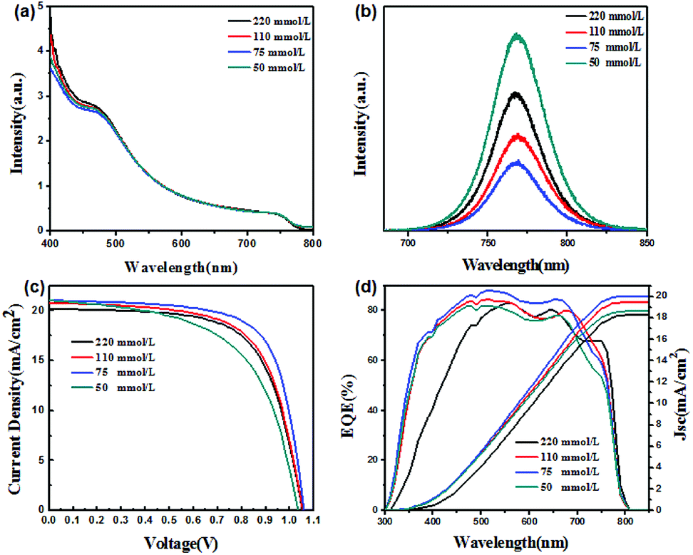 | ||
| Fig. 4 (a) Absorption spectra, (b) room-temperature photoluminescence (PL) spectra of the perovskite films based on In2S3 films with different precursor concentrations (excitation at 532 nm) and relative (c) current density–voltage curves and (d) EQE curves for perovskite solar cells based on In2S3 ETLs. | ||
To study the performance of PSCs based on In2S3 ETL in this straightforward precursor solution process, we made a comparison with the commonly used TiO2-based PSCs. First, the quality of MAPbI3 films was evaluated by crystallinity measurements. Fig. 5(a) displays the XRD patterns of the MAPbI3 films coated on In2S3 or TiO2. Both of them showed the same diffraction peaks at 14.02, 19.94, 23.36, 24.32, 28.26, 31.74, 40.56, and 43.08°, corresponding to the (110), (112), (211), (202), (220), (310), (224), and (314) crystal planes, without other impurity phases. On the other hand, the film based on In2S3 showed stronger (110), (220), and (310) diffraction peaks than TiO2, especially for the (110) peak, which revealed that the perovskite film deposited on In2S3 substrate has better crystallinity and orientation. The light absorbance spectra of the MAPbI3 films prepared based on In2S3 or TiO2 were investigated. As exhibited in Fig. 5(b), the absorbance spectra for both samples show a sharp band edge at 780 nm, which corresponds to a band gap of about 1.60 eV. Besides these, the superiority of In2S3 was also demonstrated by the photoluminescence (PL) emission results, which are shown in Fig. 5(c). Due to the enhanced electron quenching rate at the In2S3/perovskite interface, the PL intensity decreased significantly compared to that of TiO2. The time-resolved photoluminescence (TR-PL) decays of perovskite films based on In2S3 and TiO2 were measured with excitation at 325 nm (Fig. 5(d)). In2S3 exhibited time constants of τ1 = 20.860 ns and τ2 = 5.665 ns, whereas TiO2 exhibited time constants of τ1 = 64.507 ns and τ2 = 10.585 ns, which verified the faster electron injection rate from perovskite into In2S3 than into TiO2, resulting in higher electron injection quantum efficiency after electron–hole separation.
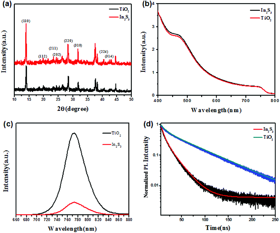 | ||
| Fig. 5 (a) XRD patterns, (b) absorption spectra, (c) room-temperature steady-state photoluminescence (PL) spectra, and (d) time-resolved photoluminescence (TR-PL) spectra of the CH3NH3PbI3 films (excitation at 325 nm and emission at 765 nm). Note: all the CH3NH3PbI3 films are coated on In2S3 and TiO2 films. | ||
Statistics analysis confirmed that PSCs based on In2S3 achieved average PCE of 13.8% on the basis of 43 devices in Fig. 6, whereas TiO2-based PSCs exhibited average efficiency of 15.1%. The little efficiency gap of In2S3-based PSCs compared to that of TiO2-based PSCs resulted from the shunt paths in the In2S3-based PSCs. Fig. 7(a) shows the J–V curves of perovskite solar cells with In2S3 and TiO2 as the ETL around the average efficiency. It can be seen that the efficiency gap between In2S3 and TiO2 exists in Jsc, whereas Voc and FF remain almost consistent. The specific parameters are listed in Table 1. On comparing the relevant parameters, it was found that the In2S3-based photovoltaic device exhibited lower shunt resistance, which illustrated that there were more shunt paths in the In2S3-based device, explaining the cause for low Jsc. Thus, we can enhance the photovoltaic efficiency by further optimizing the In2S3 thin film.
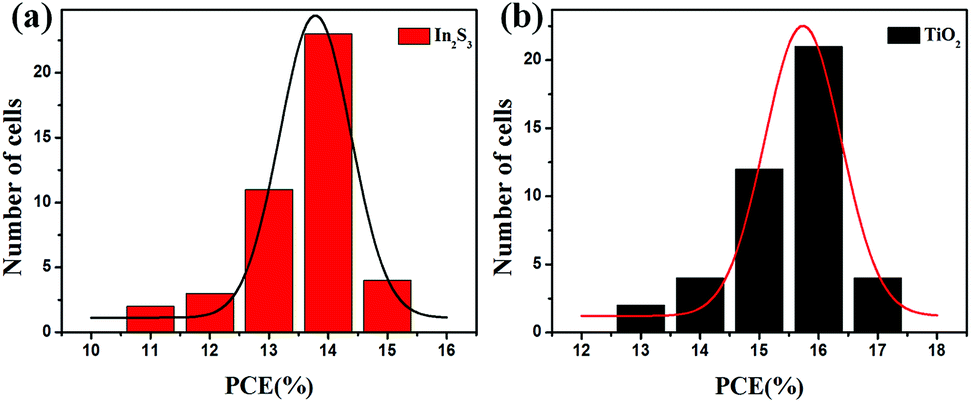 | ||
| Fig. 6 Statistical PCE distribution of perovskite solar cells based on (a) In2S3 and (b) TiO2 ETLs. | ||
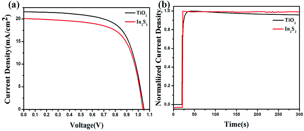 | ||
| Fig. 7 (a) The J–V characterization and (b) stability of perovskite solar cells with In2S3 and TiO2 as the ETL. | ||
| ETL type | Jsc (mA cm−2) | Voc (V) | FF (%) | PCE (%) | Rs (Ω) | Rsh (Ω) |
|---|---|---|---|---|---|---|
| TiO2 | 21.58 | 1.05 | 66.73 | 15.13 | 82.32 | 16465.43 |
| In2S3 | 20.08 | 1.04 | 67.09 | 14.02 | 76.40 | 9920.95 |
The In2S3 ETL-based device showed a faster response to photocurrent compared to the TiO2 ETL-based device. This can be ascribed to the fast trap filling process or the low density of charge traps in the CH3NH3PbI3 layer coated on In2S3 ETL. In addition, the In2S3 ETL-based device exhibited better stability compared to the TiO2-based device (Fig. 7(b)). For In2S3 ETL-based PSC, slight decrease was observed at the first few seconds and then, it remained constant, whereas the TiO2-based device exhibited a continuous descent.
Experimental
Preparation of In2S3 and TiO2 layer
In(OH)3 was used as the In source and was dissolved in carbon disulphide (CS2) and n-butylamine mixed solution, forming an In-complex precursor solution.55–57 In this system, the reaction between CS2 and n-butylamine generated butyldithiocarbamic acid (BDCA) (Fig. 1). This kind of thiol-amine acid is highly active and thus, it can react with a series of metal oxides and metal hydroxides to form an organometallic complex. First, 1 mmol In(OH)3 (99.99%, Aladdin reagent) powder was dispersed in 1 mL ethanol with magnetic stirring at room temperature. Then, 0.3 mL n-butylamine (99.5%, Aladdin reagent) was added to it. Later, 225 μL carbon disulphide (CS2) (99.9%, Aladdin reagent) was introduced into the mixed solution in a dropwise manner. The solution was further stirred for another 2 h to obtain a clear solution (Fig. 1). Here, In-complex formed is indium butyldithiocarbamates (In(S2CNHC4H9)3). The above solution was then filtered with 0.22 μm filtrator, and 1 mL filtered solution was diluted with 0.5 mL, 2 mL, 3.5 mL and 5.75 mL ethanol to form 220 mmol L−1, 110 mmol L−1, 75 mmol L−1 and 50 mmol L−1 In-complex precursors, respectively. For In2S3 thin films, different concentrations of In-complex precursor were spin-coated at a speed of 5000 rpm for 40 s on cleaned fluorine-doped tin oxide (FTO). The FTO/glass substrates were treated by UV-ozone treatment for 15 min before deposition of the In2S3 films. This was followed by annealing on a hot plate in an N2-purged glove box at 200 °C for only 1 min and at 300 °C for 2 min.TiO2 layers were grown by chemical bath deposition on cleaned FTO substrates. The deposition was made by putting the FTO/glass substrates in a glass container filled with titanium chloride solution in a 70 °C lab oven for 1 h. The deposited substrates were rinsed with deionized water for 2 min to remove any loosely bound materials, dried in a stream of N2, and annealed for 30 min at 200 °C on a hot plate.
Device assembly
The PSC adopted the structure of FTO/TiO2 or In2S3/CH3NH3PbI3/Spiro-OMeTAD/Au. All TiO2/FTO/glass substrates were treated by UV-ozone treatment for 15 min before deposition of the perovskite films. PbI2 was purchased from Alfar Aesar (99.99%), and CH3NH3I was purchased from Xi'an Polymer Light Technology Corp (99.5%). First, 1.1064 g PbI2 and 0.3816 g CH3NH3I were disolved in 1.4 mL γ-butyrolactone (GBL, 99.9%, Aldrich) and 0.6 mL dimethyl sulfoxide (DMSO, 99.9%, Aldrich) in a glovebox with constant stirring at room temperature to form the perovskite solution. Then, the perovskite solution was spin-coated on top of the ETLs (TiO2 or In2S3) at 1000 rpm for 10 s and at 4000 rpm for 40 s while dripping chlorobenzene (as the antisolvent) onto the substrate during the second spinning step. All the samples were then heated at 100 °C for 10 min, resulting in the formation of dark perovskite films. Also, 900 mg Spiro-OMeTAD (90 mg was dissolved in 1 mL chlorobenzene doped with 36 μL 4-tert-butylpyridine (TBP, Sigma-Aldrich) and 22 μL (520 mg mL−1) lithium bis imide acetonitrile solution) was deposited by spin-coating (5000 rpm for 30 s) as the hole transport layer on top of pervoskite film. Finally, a 100 nm-thick gold electrode was deposited by thermal evaporation using a shadow mask to form an active area of 9 mm2.Characterizations
X-ray diffraction was used to monitor perovskite film formation (XRD; DX-2700) via Cu-Kα radiation (λ = 1.5416 Å). The absorption spectra of the In2S3 film coated on FTO were measured by using an UV-Vis spectrometer (Lambda 950, PerkinElmer). A field emission scanning electron microscope (FESEM; SU-8020, Hitachi) was used to investigate the morphology of the perovskite films. An atomic force microscope (AFM; MULTIMODE 8, Bruker) was used to image the topography and measure the surface roughness in peak force mode. The photovoltaic performances were characterized in air without encapsulation under simulated sunlight illumination generated by a solar simulator (XES-40S2-CE, San-Ei Electric, AM 1.5 G filter at 100 mW cm−2), which was calibrated by using a certified silicon photodiode. J–V characteristics were obtained by using a source meter (2400, Keithley) at a sweep rate of 0.1 V s−1 in forward and backward scan mode.Conclusion
In conclusion, we have demonstrated a convenient, simple solution processable approach for the fabrication of In2S3 film as the ETL for high-performance planar perovskite solar cells. In2S3 ETL facilitates the injection and transport of photogenerated electrons from the perovskite absorber with reduction in charge recombination. In addition, the photoresponse rate is enhanced using In2S3 ETL compared to that obtained using TiO2. Meanwhile, In2S3 thin film used in the simplified method exhibited efficiency comparable to that of traditional TiO2 ETL in PSCs. The optimization of electron and hole transport materials and interfacial engineering are expected to further boost the conversion efficiency.Conflicts of interest
There are no conflicts to declare.Acknowledgements
The authors acknowledge support from the National University Research Fund (GK261001009), the Changjiang Scholar and Innovative Research Team (IRT_14R33), the Overseas Talent Recruitment Project (B14041) and the National Natural Science Foundation of China (61704100, 91733301).Notes and references
- Y. Cho, A. M. Soufiani, J. S. Yun, J. Kim, D. S. Lee, J. Seidel, X. Deng, M. A. Green, S. Huang and A. W. Y. Ho-Baillie, Adv. Energy Mater., 2018, 8(20), 1703392 CrossRef.
- Y.-C. Wang, J. Chang, L. Zhu, X. Li, C. Song and J. Fang, Adv. Funct. Mater., 2018, 28, 1706317 CrossRef.
- Y. Zhang, G. Grancini, Y. Feng, A. M. Asiri and M. K. Nazeeruddin, ACS Energy Lett., 2017, 2, 802 CrossRef CAS.
- D. Luo, L. Zhao, J. Wu, Q. Hu, Y. Zhang, Z. Xu, Y. Liu, T. Liu, K. Chen, W. Yang, W. Zhang, R. Zhu and Q. Gong, Adv. Mater., 2017, 29, 1604758 CrossRef PubMed.
- M. Saliba, T. Matsui, J.-Y. Seo, K. Domanski, J.-P. Correa-Baena, M. K. Nazeeruddin, S. M. Zakeeruddin, W. Tress, A. Abate, A. Hagfeldt and M. Grätzel, Energy Environ. Sci., 2016, 9, 1989 RSC.
- S.-H. Turren-Cruz, M. Saliba, M. T. Mayer, H. Juárez-Santiesteban, X. Mathew, L. Nienhaus, W. Tress, M. P. Erodici, M.-J. Sher, M. G. Bawendi, M. Grätzel, A. Abate, A. Hagfeldt and J.-P. Correa-Baena, Energy Environ. Sci., 2018, 11, 78 RSC.
- S. Wang, C. Zhang, Y. Feng, Y. Shao, Y. Yan, Q. Dong, J. Liu, B. Hu, S. Jin and Y. Shi, J. Mater. Chem. A, 2018, 6, 8860 RSC.
- NREL, Best Research-Cell Efficiences chart, http://www.nrel.gov/pv/assets/images/efficiency-chart-20180716.jpg Search PubMed.
- V. Zardetto, F. di Giacomo, H. Lifka, M. A. Verheijen, C. H. L. Weijtens, L. E. Black, S. Veenstra, W. M. M. Kessels, R. Andriessen and M. Creatore, Adv. Mater. Interfaces, 2018, 5(9), 1701456 CrossRef.
- W. Zhao, D. Yang and S. F. Liu, Small, 2017, 13, 1604153 CrossRef PubMed.
- Q.-Q. Ye, Z.-K. Wang, M. Li, C.-C. Zhang, K.-H. Hu and L.-S. Liao, ACS Energy Lett., 2018, 3, 875 CrossRef CAS.
- J. Zheng, L. Hu, J. S. Yun, M. Zhang, C. F. J. Lau, J. Bing, X. Deng, Q. Ma, Y. Cho, W. Fu, C. Chen, M. A. Green, S. Huang and A. W. Y. Ho-Baillie, ACS Appl. Energy Mater., 2018, 1, 561 CrossRef CAS.
- Z. Liu, J. Chang, Z. Lin, L. Zhou, Z. Yang, D. Chen, C. Zhang, S. F. Liu and Y. Hao, Adv. Energy Mater., 2018, 8(19), 1703432 CrossRef.
- W. Zhao, D. Yang, Z. Yang and S. Liu, Materials Today Energy, 2017, 5, 205 CrossRef.
- F. Zhang, Z. Wang, H. Zhu, N. Pellet, J. Luo, C. Yi, X. Liu, H. Liu, S. Wang, X. Li, Y. Xiao, S. M. Zakeeruddin, D. Bi and M. Grätzel, Nano Energy, 2017, 41, 469 CrossRef CAS.
- H. Yu, H. I. Yeom, J. W. Lee, K. Lee, D. Hwang, J. Yun, J. Ryu, J. Lee, S. Bae, S. K. Kim and J. Jang, Adv. Mater., 2018, 30, 1704825 CrossRef PubMed.
- Y. Zhu, K. Deng, H. Sun, B. Gu, H. Lu, F. Cao, J. Xiong and L. Li, Adv. Sci., 2018, 5, 1700614 CrossRef PubMed.
- R. Azmi, W. T. Hadmojo, S. Sinaga, C.-L. Lee, S. C. Yoon, I. H. Jung and S.-Y. Jang, Adv. Energy Mater., 2018, 8, 1701683 CrossRef.
- Z. Yang, J. Xie, V. Arivazhagan, K. Xiao, Y. Qiang, K. Huang, M. Hu, X. Yu and D. Yang, Nano Energy, 2017, 40, 345 CrossRef CAS.
- W. Yu, F. Li, H. Wang, E. Alarousu, Y. Chen, B. Lin, L. Wang, M. N. Hedhili, Y. Li, K. Wu, X. Wang, O. F. Mohammed and T. Wu, Nanoscale, 2016, 8, 6173 RSC.
- N. Wijeyasinghe, A. Regoutz, F. Eisner, T. Du, L. Tsetseris, Y.-H. Lin, H. Faber, P. Pattanasattayavong, J. Li, F. Yan, M. A. McLachlan, D. J. Payne, M. Heeney and T. D. Anthopoulos, Adv. Funct. Mater., 2017, 27, 1701818 CrossRef.
- Q. Xue, M. Liu, Z. Li, L. Yan, Z. Hu, J. Zhou, W. Li, X.-F. Jiang, B. Xu, F. Huang, Y. Li, H.-L. Yip and Y. Cao, Adv. Funct. Mater., 2018, 28, 1707444 CrossRef.
- H. Zhang, H. Wang, H. Zhu, C.-C. Chueh, W. Chen, S. Yang and A. K. Y. Jen, Adv. Energy Mater., 2018, 8(13), 1702762 CrossRef.
- I. T. Papadas, A. Savva, A. Ioakeimidis, P. Eleftheriou, G. S. Armatas and S. A. Choulis, Materials Today Energy, 2018, 8, 57 CrossRef.
- D. Ouyang, J. Xiao, F. Ye, Z. Huang, H. Zhang, L. Zhu, J. Cheng and W. C. H. Choy, Adv. Energy Mater., 2018, 8(16), 1702722 CrossRef.
- L. S. Khanzada, I. Levchuk, Y. Hou, H. Azimi, A. Osvet, R. Ahmad, M. Brandl, P. Herre, M. Distaso, R. Hock, W. Peukert, M. Batentschuk and C. J. Brabec, Adv. Funct. Mater., 2016, 26, 8300 CrossRef CAS.
- Y. Hua, P. Liu, Y. Li, L. Sun and L. Kloo, Sol. RRL, 2018, 2(5), 1700073 CrossRef.
- E. Jokar, Z. Y. Huang, S. Narra, C.-Y. Wang, V. Kattoor, C.-C. Chung and E. W.-G. Diau, Adv. Energy Mater., 2017, 8, 1701640 CrossRef.
- P. Zhao, B. J. Kim and H. S. Jung, Materials Today Energy, 2018, 7, 267 CrossRef.
- X. Zheng, H. Lei, G. Yang, W. Ke, Z. Chen, C. Chen, J. Ma, Q. Guo, F. Yao, Q. Zhang, H. Xu and G. Fang, Nano Energy, 2017, 38, 1 CrossRef CAS.
- J. Ma, G. Yang, M. Qin, X. Zheng, H. Lei, C. Chen, Z. Chen, Y. Guo, H. Han, X. Zhao and G. Fang, Adv. Sci., 2017, 4, 1700031 CrossRef PubMed.
- J. Liu, C. Gao, L. Luo, Q. Ye, X. He, L. Ouyang, X. Guo, D. Zhuang, C. Liao, J. Mei and W. Lau, J. Mater. Chem. A, 2015, 3, 11750 RSC.
- Y. Zhou, A. L. Vasiliev, W. Wu, M. Yang, S. Pang, K. Zhu and N. P. Padture, J. Phys. Chem. Lett., 2015, 6, 2292 CrossRef CAS PubMed.
- K. Lee, J. Ryu, H. Yu, J. Yun, J. Lee and J. Jang, Nanoscale, 2017, 9, 16249 RSC.
- Z. Bin, J. Li, L. Wang and L. Duan, Energy Environ. Sci., 2016, 9, 3424 RSC.
- A. F. Akbulatov, L. A. Frolova, M. P. Griffin, I. R. Gearba, A. Dolocan, D. A. Vanden Bout, S. Tsarev, E. A. Katz, A. F. Shestakov, K. J. Stevenson and P. A. Troshin, Adv. Energy Mater., 2017, 7, 1700476 CrossRef.
- Z. Wang, D. P. McMeekin, N. Sakai, S. van Reenen, K. Wojciechowski, J. B. Patel, M. B. Johnston and H. J. Snaith, Adv. Mater., 2016, 5, 1604186 Search PubMed.
- Y.-C. Wang, X. Li, L. Zhu, X. Liu, W. Zhang and J. Fang, Adv. Energy Mater., 2017, 7, 1701144 CrossRef.
- Z. Zhu, J. Q. Xu, C. C. Chueh, H. Liu, Z. Li, X. Li, H. Chen and A. K. Jen, Adv. Mater., 2016, 28, 10786 CrossRef CAS PubMed.
- M. A. Mahmud, N. K. Elumalai, M. B. Upama, D. Wang, K. H. Chan, M. Wright, C. Xu, F. Haque and A. Uddin, Sol. Energy Mater. Sol. Cells, 2017, 159, 251 CrossRef CAS.
- J. Ma, X. Zheng, H. Lei, W. Ke, C. Chen, Z. Chen, G. Yang and G. Fang, Sol. RRL, 2017, 1, 1700118 CrossRef.
- E. Halvani Anaraki, A. Kermanpur, M. T. Mayer, L. Steier, T. Ahmed, S.-H. Turren-Cruz, J. Seo, J. Luo, S. M. Zakeeruddin, W. R. Tress, T. Edvinsson, M. Grätzel, A. Hagfeldt and J.-P. Correa-Baena, ACS Energy Lett., 2018, 3, 773 CrossRef CAS.
- W.-Q. Wu, D. Chen, Y.-B. Cheng and R. A. Caruso, Sol. RRL, 2017, 1, 1700117 CrossRef.
- Y. Lee, S. Paek, K. T. Cho, E. Oveisi, P. Gao, S. Lee, J.-S. Park, Y. Zhang, R. Humphry-Baker, A. M. Asiri and M. K. Nazeeruddin, J. Mater. Chem. A, 2017, 5, 12729 RSC.
- K. Wang, Y. Shi, Q. Dong, Y. Li, S. Wang, X. Yu, M. Wu and T. Ma, J. Phys. Chem. Lett., 2015, 6, 755 CrossRef CAS PubMed.
- P. Chen, X. Yin, M. Que, X. Liu and W. Que, J. Mater. Chem. A, 2017, 5, 9641 RSC.
- C. D. Wessendorf, J. Hanisch, D. Müller and E. Ahlswede, Sol. RRL, 2018, 2(5), 1800056 CrossRef.
- W. Zhao, Z. Yao, F. Yu and F. Liu, Part. Part. Syst. Charact., 2018, 35(8), 1800137 CrossRef.
- Z. Guo, W. Hu, T. Liu, X. Yin, X. Zhao, S. Luo, Y. Guo, Z. Yao, N. Wang, H. Lin, J. Wang and H. Liu, J. Mater. Chem. A, 2016, 5, 1434 Search PubMed.
- W.-Q. Wu, D. Chen, F. Li, Y.-B. Cheng and R. A. Caruso, Materials Today Energy, 2018, 7, 260 CrossRef.
- W. Li, Q. Jiang, J. Yang, Y. Luo, X. Li, Y. Hou and S. Zhou, Sol. Energy Mater. Sol. Cells, 2017, 159, 143 CrossRef CAS.
- W.-Q. Wu, D. Chen, Y.-B. Cheng and R. A. Caruso, J. Mater. Chem. A, 2017, 5, 10092 RSC.
- J. Feng, Z. Yang, D. Yang, X. Ren, X. Zhu, Z. Jin, W. Zi, Q. Wei and S. Liu, Nano Energy, 2017, 36, 1 CrossRef CAS.
- Y. Hou, X. Chen, S. Yang, Y. L. Zhong, C. Li, H. Zhao and H. G. Yang, Nano Energy, 2017, 36, 102 CrossRef CAS.
- W. Zhao, Y. Cui and D. Pan, Energy Technol., 2013, 1, 131–134 CrossRef CAS.
- W. Zhao, G. Wang, Q. Tian, L. Huang, S. Gao and D. Pan, Sol. Energy Mater. Sol. Cells, 2015, 133, 15–20 CrossRef CAS.
- W. Zhao, D. Pan and S. Liu, CrystEngComm, 2016, 18, 4744–4748 RSC.
Footnote |
| † Electronic supplementary information (ESI) available: TG curves, XPS, SEM-EDX UPS, and AFM height image of In2S3 thin film, AFM height images of perovskite thin films, the best PSC device parameters table, PCE distribution image and cross-sectional SEM image of the perovskite solar cells are exhibited. See DOI: 10.1039/c8ra08940j |
| This journal is © The Royal Society of Chemistry 2019 |