
 Open Access Article
 This Open Access Article is licensed under a Creative Commons Attribution-Non Commercial 3.0 Unported Licence
Photo-enhanced gas sensing of SnS2 with nanoscale defects†
Wen-Jie Yana,
Deng-Yun Chena,
Huei-Ru Fuh*bc,
Ying-Lan Lia,
Duan Zhanga,
Huajun Liud,
Gang Wua,
Lei Zhang e,
Xiangkui Rene,
Jiung Chof,
Miri Choig,
Byong Sun Chunh,
Cormac Ó. Coileáina,
Hong-Jun Xua,
Zhi Wanga,
Zhaotan Jianga,
Ching-Ray Chang*b and
Han-Chun Wu*a
e,
Xiangkui Rene,
Jiung Chof,
Miri Choig,
Byong Sun Chunh,
Cormac Ó. Coileáina,
Hong-Jun Xua,
Zhi Wanga,
Zhaotan Jianga,
Ching-Ray Chang*b and
Han-Chun Wu*a
aSchool of Physics, Beijing Institute of Technology, Beijing 100081, P. R. China. E-mail: wuhc@bit.edu.cn
bDepartment of Physics, National Taiwan University, Taipei 106, Taiwan. E-mail: crchang@phys.ntu.edu.tw
cDepartment of Chemical Engineering & Materials Science, Yuan Ze University, Taoyuan City 320, Taiwan. E-mail: hrfuh@saturn.yzu.edu.tw
dInstitute of Plasma Physics, Chinese Academy of Sciences, Hefei 230031, P. R. China
eSchool of Chemical Engineering and Technology, Tianjin University, Tianjin 300072, P. R. China
fWestern Seoul Center, Korea Basic Science Institute, Seoul 03579, Republic of Korea
gChuncheon Center, Korea Basic Science Institute, Chuncheon 24341, Republic of Korea
hDivision of Industrial Metrology, Korea Research Institute of Standards and Science, Daejeon 305-340, Republic of Korea
First published on 2nd January 2019
Abstract
Recently a SnS2 based NO2 gas sensor with a 30 ppb detection limit was demonstrated but this required high operation temperatures. Concurrently, SnS2 grown by chemical vapor deposition is known to naturally contain nanoscale defects, which could be exploited. Here, we significantly enhance the performance of a NO2 gas sensor based on SnS2 with nanoscale defects by photon illumination, and a detection limit of 2.5 ppb is achieved at room temperature. Using a classical Langmuir model and density functional theory simulations, we show S vacancies work as additional adsorption sites with fast adsorption times, higher adsorption energies, and an order of magnitude higher resistance change compared with pristine SnS2. More interestingly, when electron–hole pairs are excited by photon illumination, the average adsorption time first increases and then decreases with NO2 concentration, while the average desorption time always decreases with NO2 concentration. Our results give a deep understanding of photo-enhanced gas sensing of SnS2 with nanoscale defects, and thus open an interesting window for the design of high performance gas sensing devices based on 2D materials.
Nitrogen dioxide (NO2) is one of the most common hazardous gas pollutants produced as a by-product of industry.1–4 Notably, NO2 is also a product yielded from the thermal decomposition of organic nitrates, such as TNT, which is a useful fingerprint for controlling these substances and combating international terrorism.5 An issue of global concern, serious respiratory diseases can be caused by chronic environmental exposure to as little as 53 ppb NO2.1,4,6 Therefore, the research and development of gas sensors with high sensitivities is always of high priority.2,7–19 Recently, 2D materials have been used for gas sensing owing to their large surface-to-volume ratios.13,20 A wide variety of 2D materials, such as graphene,9,10,14 black phosphorus,2,21 metal dichalcogenides,4,12,15,18,19,22–24 have been studied as high performance gas sensors.16,20,23,25,26
As a member of the wide class 2D materials, tin disulfide (SnS2) displays many intriguing properties in electronics,27 photonics and optoelectronics,27–30 as well as gas monitoring.24,31–42 It was reported recently by Kalantar-zadeh et al. that a SnS2-based NO2 gas sensor with a sensitivity of 0.5 ppm could be improved to 30 ppb when heated to 120 °C.24 However, an elevated operating temperature typically increases power consumption and thus a more intricate setup is required.3,10,16,20,24,25,43 Furthermore, the high operating temperature might pose the risk of ignition when detecting in flammable or explosive atmospheres which would limit sensor's application.44–46 Concurrently, it is known that 2D materials produced by chemical vapor deposition (CVD) usually contain nanoscale defects, such as vacancies, grain boundaries, etc. and in particular CVD grown SnS2 is reported to naturally contain S vacancies.47 It is well known that nanoscale defects can significantly affect gas sensing performance.48 Thus it is important to investigate how S vacancies in SnS2 affect the gas sensing performance. Furthermore, it should be also noted that compared with thermally assisted gas sensing, a photon assisted arrangement can not only improve the detection limit of gas sensor but also can accelerate the desorption ratio.15,19,49–51 It is reported that SnS2 nanosheets exhibit excellent optoelectronics properties,27–30 making it feasible to improve the gas sensing performance of SnS2 with photon illumination.
In this work, we demonstrate that photon illumination can significantly enhance the performance of NO2 gas sensors based on SnS2, and an ultra-low concentration sensitivity of 2.5 ppb is achieved at room temperature. The results also show that gas sensitivity increases linearly with decreasing SnS2 nanosheet thickness. In combination with a classical Langmuir model and density functional theory simulations, we show that S vacancies work as additional adsorption sites with fast adsorption times, higher adsorption energies, and greater resistance change compared with pristine SnS2. Moreover, when electron–hole pairs are excited by photon illumination, the average adsorption time first increases and then decreases with NO2 concentration. Considering safety, energy efficiency and sensitivity, SnS2-based photo-illuminated gas sensors provide a possible way to realize the measurement of ultra-low concentrations of NO2, or other hazardous gases, for environmental, industrial and domestic monitoring.
Fig. 1(a) shows a schematic of the chemical vapor deposition (CVD) arrangement for the SnS2 nanosheet growth. A sulfur powder source was placed upstream in the furnace. Sn granules were smashed into pieces and were placed at the center of the furnace. Several pieces of a diced 300 nm SiO2/Si (1 cm × 1 cm) wafer were placed downstream as substrates for SnS2 growth. Further details of the SnS2 growth can be found in the Experimental section. After the reaction, SnS2 nanosheets were formed on the SiO2/Si substrates. Fig. 1(b) shows a scanning electron microscopy (SEM) image of a SnS2 flake grown on a SiO2/Si substrate. The flakes typically have a semi-hexagonal structure with lateral dimensions ranging from 10 μm to 228 μm (Fig. S1†). Fig. 1(c) gives the structure of SnS2 with the purple and yellow spheres representing Sn and S atoms, respectively.
 | ||
| Fig. 1 (a) A schematic of CVD growth setup. (b) A SEM image of a semi-hexagonal nanosheet of SnS2. (c) Schematic of SnS2 structure with purple and yellow spheres representing Sn and S atoms, respectively. | ||
Atomic force microscopy (AFM) was used to determine the thicknesses of the nanosheets. Fig. 2(a) shows the height profile of an ultrathin SnS2 nanosheet with a thickness ≈ 6 nm (≈10 layers, 0.6 nm per layer),30 as measured along the red dotted line in the inset image, (more examples in Fig. S2†). The SnS2 was also characterized by Raman spectroscopy, as shown in Fig. 2(b). Only a single Raman peak (A1g mode at 314 cm−1) can be clearly observed for an 8 nm thick SnS2 nanosheet, and an additional Raman peak, the Eg mode at 205 cm−1, appears for a thicker 60 nm SnS2 nanosheet, which is consistent with literature.28,52 The Eg mode is due to the scattering centers for in-plane scattering. When the thickness drops below 8 nm the intensity decreases and effectively becomes undetectable.30 The crystal structure of few-layer SnS2 was further characterized by high-resolution transmission electronic microscopy (HRTEM), indicating the single-crystalline structure of the SnS2 (Fig. 2(c)). The measured width of the lattice fringes is ≈0.32 nm which corresponds to the (100) plane of SnS2. Fig. 2(d) shows the selected-area-electron-diffraction (SAED) pattern, which displays six-fold symmetry diffraction spots, confirming the hexagonal single-crystalline nature of the flake. Additionally, Sn and S elemental mapping using Electron Energy Loss Spectroscopy (EELS), in Fig. 2(f), of the selected area shown in Fig. 2(e), indicates the atomic ratio of Sn![[thin space (1/6-em)]](https://www.rsc.org/images/entities/char_2009.gif) :S ≈ 1:1.86, suggesting the presence of S vacancies in the SnS2, which is consistent with earlier reports.47
:S ≈ 1:1.86, suggesting the presence of S vacancies in the SnS2, which is consistent with earlier reports.47
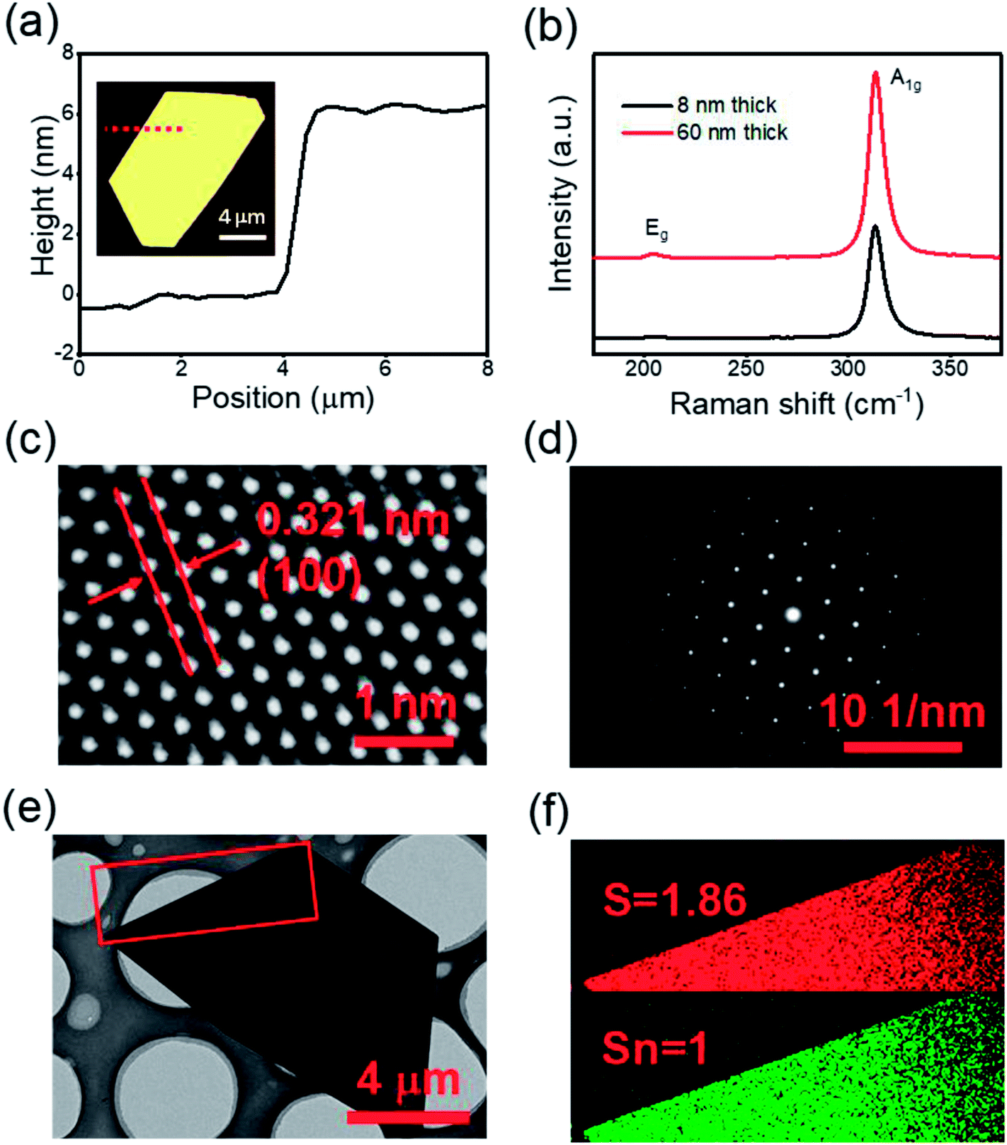 | ||
| Fig. 2 Characterization of CVD produced single crystal SnS2 nanosheet. (a) Height profiles of the dashed line shown in the inset AFM image. (b) Raman spectra of SnS2 nanosheet. (c) High-resolution TEM image and corresponding (d) selected-area-electron-diffraction (SAED) pattern of a typical grown SnS2 flake. (e) Low magnification bright field TEM image of a semi-hexagonal SnS2 nanosheet. (f) EELS elemental mapping of the selected area in (e) with the result Sn:S = 1:1.86. | ||
Before studying the photo-enhanced gas sensing properties of SnS2, we first explored its optoelectronic properties. Fig. 3(a) is an optical image of a typical device prepared from a semi-hexagonal SnS2 nanosheet on a SiO2/Si substrate with 300 nm thick SiO2. Fig. 3(b) shows the current versus voltage IDS–VDS (DS, Drain–Source) characteristics of the device with the gate voltage (VG) varied from −20 V to 20 V in steps of 5 V and Fig. 3(c) plots the relationship between IDS and VG, with VDS ranging from −10 V to +10 V in steps of 2.5 V indicating transfer characteristics of the device. From Fig. 3(b and c) it is apparent that our CVD grown SnS2 nanosheets are n-type and the mobility is around 9.7 cm2 V−1 s−1 which further supports the presence of the S vacancies.47 Fig. 3(d and e) shows the I–V characteristics of the device at VG = 0 V in the dark and under illumination by 532 nm and 650 nm lasers, in ambient conditions. It is found there is a notable change in the IDS response going from dark to illuminated, and the enhancement of IDS for the 532 nm laser is relatively larger than that observed for the 650 nm laser. Fig. 3(f) further shows the time resolved photo response of another device at VDS = 5 V, where the light intensity of the 532 nm laser was 3.0 mW cm−2. The responsivity (Rλ) and external quantum efficiency (EQE) are calculated to be 31 A W−1 and 7.7 × 10³%, respectively (details of this calculation can be found in ESI Formula (2)†).
 | ||
| Fig. 3 (a) Optical microscope image of a SnS2 device for the following measurement. (b) IDS–VDS curves for different VG from −20 to 20 V in steps of 5 V. (c) IDS–VG curves for different VDS from −10 to 10 V in steps of 2.5 V. (d) IDS–VDS curves of device under 532 nm laser illumination by different energy densities. (e) IDS–VDS curves of device under 650 nm laser illumination by different energy densities. (f) Time-resolved photon response of another SnS2 device measured in vacuum (VDS = 5 V, 532 nm laser 0.979 mW cm−2). | ||
Fig. 4(a) is an optical image of a typical SnS2-based gas sensor fabricated by conventional UV-lithography. The distance between each of the contacts is approximately 5 μm. Fig. 4(b and c) show the dynamic-sensing responses without and with 405 nm laser irradiation, respectively, where the NO2 gas concentration was varied from 6.5 ppb to 130 ppb. The sensor response is defined as ΔR/R0 = (RNO2 − RN2)/RN2, where RN2 and RNO2 are the resistances of the device when exposed to pure N2 and a NO2 gas mix, respectively. In the dark environment, the sensor has the first observable response at 78 ppb NO2. Remarkably, by illuminating the sensor with a 405 nm laser a clear response is observed at 13 ppb NO2. To confirm this, Fig. 4(d) plotted IDS–VDS curves of the same device under different NO2 concentrations. It is apparent that in the dark environment, the IDS–VDS curves for 0 ppb, 26 ppb and 52 ppb NO2 merge together. In contrast with this, clear distinctions can be observed between 0 ppb, 26 ppb and 52 ppb NO2 with 405 nm laser illumination. A similar effect was observed with 650 nm (26 ppb) and 785 nm (52 ppb) lasers (Fig. S3†). Thus, laser illumination can improve the gas sensing capabilities of such devices.
 | ||
| Fig. 4 (a) Optical microscope image of a SnS2 device for gas sensor measurements. Dynamic sensing response of ΔR/R0 change versus time for the SnS2-based sensor upon exposure to NO2 gas with concentrations ranging from 6.5 ppb to 130 ppb under (b) dark environment and (c) 405 nm laser irradiation. (d) Comparison IDS–VDS curves of the device under different light illuminations and NO2 concentrations. (e) Multi-cycle responses of sensor when exposed to concentrations of 13, 39, and 78 ppb NO2. (f) Sensitivity as a function of SnS2 thickness. | ||
The stability of a sensor is critical for practical applications. Multi-cycle dynamic sensing responses of the SnS2-based sensor against to 13, 39 and 78 ppb NO2 are used here to demonstrate the good repeatability and reproducibility of such SnS2-based sensors (Fig. 4(e)). Moreover, the response to varied concentrations of NO2 with a relative humidity 64% is also showed in Fig. S5(d).† These indicate the reliability of the illuminated SnS2-based sensor and that the presence of water does not degrade performance.
To probe the function of sensitivity versus the thickness of SnS2, we also tested more than 10 samples with different thicknesses, ranging from 17 nm to 370 nm (Fig. S4–S9†). It is found that the sensitivity increases linearly as the thickness of the SnS2-nanosheets is reduced, as shown in Fig. 4(f). Remarkably, a significant response is unmistakably observed at 2.5 ppb NO2 for a 22 nm thick SnS2 based gas sensor (Fig. S8(d)†), suggesting that SnS2 based gas sensor can achieve a NO2 detection limit better than 2.5 ppb. To the best of our knowledge, this is the lowest detection limit for NO2 achieved using SnS2 devices to date, which is an improvement by a factor greater than ten on previous work.24 Table 1 summarizes and compares the important features of SnS2-based NO2 gas sensors from literature. Kalantar-zadeh et al. heated their SnS2 flake sensor to 120 °C to achieve a 30 ppb detection limit.24 Hao et al. heated a SnS2 flower interspersed with SnO2 to 100 °C to reach a 125 ppb detection limit.31 Ahn et al. built utilized vertical SnS2 flake structures to detect NO2 at 300 ppb, probably under its optimum conditions at 160 °C.39 Li et al. heated SnS2 their flake devices to 120 °C to attain a 600 ppb detection limit.40 Wang et al. heated a SnS2–SnO2 composite flake device to 80 °C for a 1000 ppb detection limit.41 While Xue et al. used SnS1.5/Se0.5 flake devices to detect 1000 ppb NO2 at room temperature.42
| No. | Material | Limit of detection | Special method | Reference |
|---|---|---|---|---|
| 1 | SnS2 flake | 2.5 ppb | UV illumination | This work |
| 2 | SnS2 flake | 30 ppb | Heater | 24 |
| 3 | SnS2/SnO2 flakes | 125 ppb | Heater | 31 |
| 4 | SnS2 flakes | 300 ppb | Heater | 39 |
| 5 | SnS2 flakes | 600 ppb | Heater | 40 |
| 6 | SnS2/SnO2 | 1000 ppb | Heater | 41 |
| 7 | SnS1.5/Se0.5 | 1000 ppb | Room temperature | 42 |
To better illustrate the photo-enhanced gas sensing properties, we summarized the signal/noise (S/N) ratios of the ΔR/R0 from response in Fig. 4(b and c) into Fig. 5(a).53–57 It is clear that there are 3 distinct regions. At high concentrations of NO2 the S/N is almost constant (dark and 785 nm). This means the surface adsorption is almost saturated and has reached its upper limit. Increasing gas concentration does not increase the signal. In the medium concentration range (classic region), S/N increases linearly with gas concentration. In the low NO2 concentration regime (<52 ppb) no effective signal is detected for dark conditions. But a signal is detected with illumination, which is especially prominent for the short wavelength light, indicating extra energy is required to desorb NO2 from surface of SnS2.
 | ||
| Fig. 5 (a) Comparison of S/N ratio of the dynamic response of the SnS2 sensor for dark and illuminated environments. Green line is a linear fitting of dark environment data between 52 to 130 ppb NO2. Black line and blue line are linear fitting of 405 nm illumination data between 6.5 to 52 ppb and 52 to 130 ppb NO2. (b) Desorption time as a function of gas concentration. (c) Adsorption time as a function of gas concentration. | ||
We fitted the desorption (adsorption) sections of the dynamic-sensing response curves under different laser illuminations with the expression  where τD (τA) is the average desorption (adsorption) time. The average desorption times and average adsorption times under various laser illuminations are summarized in Fig. 5(b) and (c) respectively. It is clear illumination not only enables ultra-high sensitivity but also results in faster desorption and better S/N ratios. Interestingly, with the 405 nm laser illumination, the adsorption time first increases and then decreases with gas concentration when the concentration reaches ∼78 ppb. While for dark and 785 nm laser illumination, both the desorption and adsorption times decrease with increasing gas concentration.
We replotted the dynamic-sensing response curves under 405 nm laser illumination based on the Langmuir model (Fig. 6).58 There are two classes of adsorption sites. Similar behavior has been observed under 785 nm and 650 nm laser illumination (Fig. S10†). For the adsorption process, NO2 can adsorb on both sites but prefer sites with fast adsorption times. With increasing gas concentration, more NO2 molecules will be adsorbed on sites with slower adsorption times which increases the average adsorption time. At yet higher gas concentrations all the fast adsorption time sites will be occupied. The NO2 molecules will be adsorbed on the sites with slow adsorption times, which can be treated as one site adsorption. According to the Langmuir model considering one adsorption site,  where Nc is proportional to the gas concentration. This is why the average adsorption time first increases and then decreases with gas concentration. On the other hand, for the desorption process at low concentrations it is the sites with slow desorption times that are the limiting factor. With increasing gas concentration, more molecules will be desorbed from the sites with faster desorption times, thus decreasing the average desorption time. Moreover, NO2 molecules absorb on sites with faster adsorption times will significantly decrease the overall conductance compared with NO2 molecules bound to sites with slow adsorption.
 | ||
| Fig. 6 The dI/dt–I relationship of Fig. 4(c). (a) The dI/dt–I curve of 17.5 ppb NO2 test. (b) The dI/dt–I curve of 54 ppb NO2 test. In both of two picture, the fitting lines are shown, with blue line depicting the fast desorption process, violet line depicting slow desorption process, red line depicting fast adsorption process and green line depicting slow adsorption process. | ||
To investigate whether S vacancies could give such an effect, we calculated the adsorption energy, charge density distribution, and conductance of NO2 molecules on a SnS2 monolayer with and without S vacancies. Details of the calculations can be found in the Methods section. Fig. 7(a) and (b) show the optimized atomic structures of a NO2 molecule adsorbed on pristine SnS2 and SnS2 with a surface S vacancy respectively. For a NO2 molecule adsorbed on pristine SnS2, the perpendicular distance between the O atom of a NO2 molecule and the nearest S atom of the SnS2 (R) is about 2.95 Å and it is decreased significantly to 0.5 Å for a NO2 molecule on SnS2 with a S vacancy, indicating the S vacancy induces strong adsorption between SnS2 and NO2. To understand the adsorption mechanism, the adsorption energy as a function of distance R is plotted in Fig. 7(c). The adsorption energy is 1.011 eV when a NO2 molecule adsorbed on SnS2 with a S vacancy. While for a NO2 molecule adsorbed on pristine SnS2, the corresponding adsorption energy is only 116 meV. Thus, NO2 molecules adsorbed on the SnS2 monolayer with S vacancies have a larger adsorption energy compared with a pristine SnS2 monolayer, indicating that extra energy is required to desorb NO2 molecule from the S vacancy site (Fig. 7(d)). The adsorption energy for chemisorption is usually an energy of 1–10 eV, but for physisorption the energy is smaller than this. Therefore, the adsorption mechanism may change from physisorption to chemisorption when a NO2 molecule adsorbed on SnS2 with S vacancy. Moreover, there is a large partial charge transfer between S and the O atoms of a NO2 molecule adsorbed on SnS2 with S vacancy in Fig. 7(e) and (f).
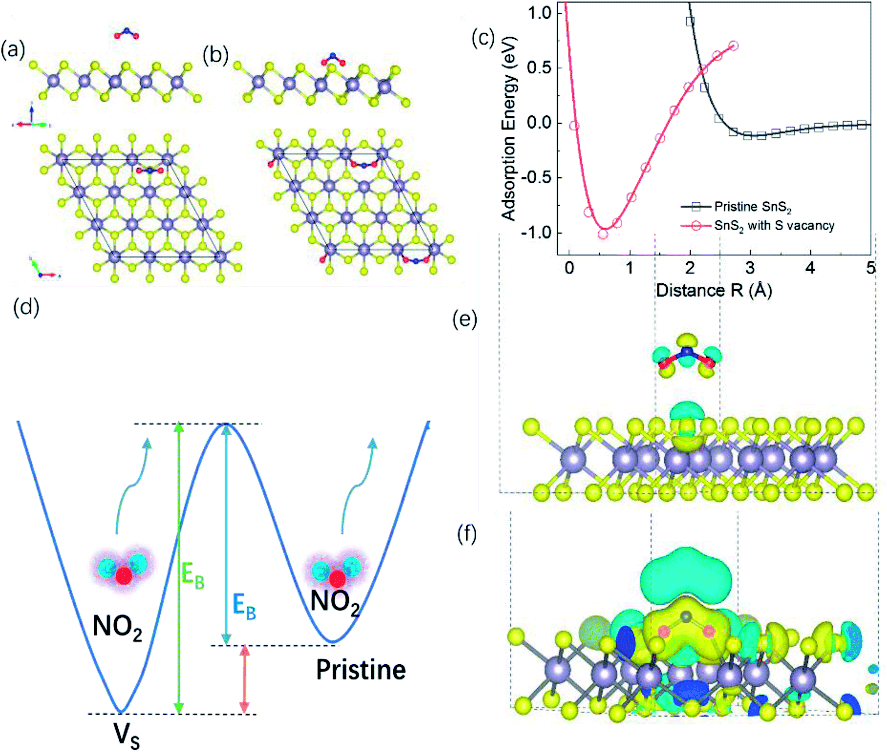 | ||
| Fig. 7 (a) and (b) Side view and top view of the atomic structure of NO2 molecule adsorbed on Sn9S18 and Sn9S17 surfaces, respectively. The large dark spheres represents Sn atoms, while the yellow, blue and red spheres represent the S, N and O atoms, respectively. (c) Adsorption energy as a function of distance R (defined as the perpendicular distance between the O atom of NO2 molecule and the nearest S atom of the SnS2) for NO2 molecule adsorbed on Sn9S18 and Sn9S17 surfaces. (d) Schematic of adsorption energies for an NO2 molecule adsorbed on pristine SnS2 and on SnS2 with a S vacancy. (e) and (f) Charge density difference distribution for NO2 molecule adsorbed on Sn9S18 and Sn9S17 surfaces, respectively. The charge density difference in yellow indicate increases in charge density, while blue indicates a decreases in charge density (isosurface = 0.0015 eV A−3). | ||
The electrical conductivity of an NO2 molecule adsorbed on pristine SnS2 and on SnS2 with a single S vacancy at 300 K are shown in Fig. 8. We found that monolayer SnS2 contains a narrow electrical conductivity tail near μ = 0 resulting from electrons crossing the Fermi level from thermal agitation at T = 300 K, shown in Fig. 8(a). When this pristine SnS2 adsorbs an NO2 molecule there is an additional conductivity peak region near μ = 0 with small values of 1.1 × 10³ and 3.0 × 10² (1/Ω m−1) for σxx and σyy, respectively, as shown in Fig. 8(b). However for SnS2 with a S vacancy adsorbing a NO2 molecule, there is a broad additional conductivity region around μ = 0 with values about 1.5 × 10⁴ and 1.9 × 10⁴ (1/Ω m−1) for σxx and σyy, respectively, shown in Fig. 8(c). These results from transport and DFT analysis are consistent with the experimental conclusions on the resistance changes, and also indicate charge transfer between NO2 and SnS2 is critical. It also suggests that the sites with fast adsorption times are S vacancies and the sites with slow adsorption times are the areas of pristine SnS2. To further highlight the importance of S vacancies for the gas sensor performance, we measured the gas performance of gas sensors based on same thick SnS2 but with different S vacancy density, where the density of S vacancies density was determined by mapping the whole sensor using the EDS equipped in the SEM chamber. A relatively low detection limit or high gas performance was achieved for the sample with higher S vacancies density. For example, for gas sensors based one 106 nm thick SnS2, the detection limit for sensor with an atomic ratio of Sn:S ≈ 1:1.72 is 6.5 ppb and that for sensor with an atomic ratio of Sn:S ≈ 1:1.84 is 13 ppb. We would like to stress that the nanoscale defects are naturally occurring defects forming during chemical vapor deposition. Therefore, they are quite stable when interacting with NO2 molecules.
 | ||
| Fig. 8 Electron conductivity of (a) SnS2 monolayer (b) SnS2 with adsorbed NO2 molecule and (c) SnS2 with S vacancy adsorbed NO2 molecule which S vacancy concentration is 3.70% at 300 K. | ||
It is reported that Schottky junction59,60 and photo-excited electron–hole pairs can contribute the gas sensing performance. Since our gas sensing performance depends crucially on the wavelength of the photons and same bias voltage is used, here we focus our discussion on effect due to photo-excited electron–hole pairs. We measured the gas sensing performance of another sensor under 365, 405, and 650 nm laser illuminations (Fig. S11†). Only 365 and 405 nm lasers can excite electron–hole pairs, because the band gap of SnS2 is around 2.2 eV. The 365 and 405 nm laser illuminations have similar detection limit, better than 650 nm. More importantly, the average adsorption time first increases and then decreases with NO2 concentration under the 365 and 405 nm laser illuminations, indicating the importance of photo-excited electron–hole pairs for the charge transfer process upon NO2 adsorption. Therefore, the observed distinct behavior of the adsorption time may be due to the photo-excited electron–hole pairs. We would like to stress that the average adsorption time is faster under the 405 nm photo illumination than the 365 nm, indicating that the 405 nm laser illumination is more efficient since the adsorption spectrum of NO2 peaks at ∼400 nm at 293 K.61
In summary, NO2 gas sensors were fabricated based on CVD grown SnS2. An ultra-high sensitivity of 2.5 ppb at room temperature was achieved by utilizing inherent defects under photon illumination. Our results further show S vacancies in SnS2 work as additional adsorption sites and the detection limit, signal to noise (S/N) value, and desorption time can be significantly improved by photo illumination, thus providing a plausible way to design high performance gas sensors based on 2D materials with nanoscale defects.
Method
The detailed experiments and characterizations are shown in the ESI.†Author contributions
H. C. W. conceived the study. D. Y. C., and Y. L. L. grew the sample. W. J. Y., H. J. X. and Z. W. fabricated the sample. J. C., M. C., and B. S. C. carried out the TEM measurements. W. J. Y. and C. C. performed the gas sensing measurements. H. R. F. and C. R. C. conducted the DFT simulation. Z. T. J. and H. J. L. gave scientific advice. H. C. W., W. J. Y., D. Y. C., and C. C. wrote the manuscript. All authors discussed the results and commented on the manuscript.Conflicts of interest
There no conflicts to declare.Acknowledgements
This work was supported by the National Key R&D Program of China (Grant No. 2017YFE0301404 and 2017YFA0303800), the National Natural Science Foundation of China (No. 61874010, 11804237), and by the Science and Technology Innovation Program for Creative Talents in Beijing Institute of Technology (No. 2017CX01006).References
- B. Liu, L. Chen, G. Liu, A. N. Abbas, M. Fathi and C. Zhou, ACS Nano, 2014, 8(5), 5304–5314 CrossRef CAS PubMed.
- A. N. Abbas, B. Liu, L. Chen, Y. Ma, S. Cong, N. Aroonyadet, M. Köpf, T. Nilges and C. Zhou, ACS Nano, 2015, 9(5), 5618–5624 CrossRef CAS PubMed.
- S. S. Shendage, V. L. Patil, S. A. Vanalakar, S. P. Patil, N. S. Harale, J. L. Bhosale, J. H. Kim and P. S. Patil, Sens. Actuators, B, 2017, 240, 426–433 CrossRef CAS.
- T. Xu, Y. Pei, Y. Liu, D. Wu, Z. Shi, J. Xu, Y. Tian and X. Li, J. Alloys Compd., 2017, 725, 253–259 CrossRef CAS.
- C. Hao, P. B. Shepson, J. W. Drummond and K. Muthuramu, Anal. Chem., 1994, 66(21), 3737–3743 CrossRef CAS.
- https://www.epa.gov/criteria-air-pollutants/naaqs-table.
- J. Kong, N. R. Franklin, C. Zhou, M. G. Chapline, S. Peng, K. Cho and H. Dai, Science, 2000, 287(5453), 622–625 CrossRef CAS PubMed.
- E. Rossinyol, A. Prim, E. Pellicer, J. Arbiol, F. Hernández-Ramírez, F. Peiró, A. Cornet, J. R. Morante, L. A. Solovyov, B. Tian, T. Bo and D. Zhao, Adv. Funct. Mater., 2007, 17(11), 1801–1806 CrossRef CAS.
- F. Schedin, A. K. Geim, S. V. Morozov, E. W. Hill, P. Blake, M. I. Katsnelson and K. S. Novoselov, Nat. Mater., 2007, 6(9), 652–655 CrossRef CAS.
- J. D. Fowler, M. J. Allen, V. C. Tung, Y. Yang, R. B. Kaner and B. H. Weiller, ACS Nano, 2009, 3(2), 301–306 CrossRef CAS PubMed.
- S. Deng, V. Tjoa, H. M. Fan, H. R. Tan, D. C. Sayle, M. Olivo, S. Mhaisalkar, J. Wei and C. H. Sow, J. Am. Chem. Soc., 2012, 134(10), 4905–4917 CrossRef CAS PubMed.
- F. K. Butt, C. Cao, W. S. Khan, Z. Ali, R. Ahmed, F. Idrees, I. Aslam, M. Tanveer, J. Li and S. Zaman, Mater. Chem. Phys., 2012, 137(137), 565 CrossRef CAS.
- F. K. Perkins, A. L. Friedman, E. Cobas, P. M. Campbell, G. G. Jernigan and B. T. Jonker, Nano Lett., 2013, 13(2), 668–673 CrossRef CAS.
- W. Yuan, A. Liu, L. Huang, C. Li and G. Shi, Adv. Mater., 2013, 25(5), 766–771 CrossRef CAS PubMed.
- N. Huo, S. Yang, Z. Wei, S.-S. Li, J.-B. Xia and J. Li, Sci. Rep., 2014, 4, 5209 CrossRef CAS PubMed.
- H. Long, A. Harley-Trochimczyk, T. Pham, Z. Tang, T. Shi, A. Zettl, C. Carraro, M. A. Worsley and R. Maboudian, Adv. Funct. Mater., 2016, 26(28), 5158–5165 CrossRef CAS.
- J. Zhang, X. Liu, G. Neri and N. Pinna, Adv. Mater., 2016, 28(5), 795–831 CrossRef CAS.
- J. Baek, D. Yin, N. Liu, I. Omkaram, C. Jung, H. Im, S. Hong, S. M. Kim, Y. K. Hong, J. Hur, Y. Yoon and S. Kim, Nano Res., 2017, 10(8), 2904 CrossRef CAS.
- Z. Feng, Y. Xie, E. Wu, Y. Yu, S. Zheng, R. Zhang, X. Chen, C. Sun, H. Zhang, W. Pang, J. Liu and D. Zhang, Micromachines, 2017, 8(5), 155 CrossRef.
- B. Cho, J. Yoon, S. K. Lim, A. R. Kim, D.-H. Kim, S.-G. Park, J.-D. Kwon, Y.-J. Lee, K.-H. Lee, B. H. Lee, H. C. Ko and M. G. Hahm, ACS Appl. Mater. Interfaces, 2015, 7(30), 16775–16780 CrossRef CAS PubMed.
- L. Kou, T. Frauenheim and C. Chen, J. Phys. Chem. Lett., 2014, 5(15), 2675–2681 CrossRef CAS PubMed.
- S. Weidong, H. Lihua, W. Haishui, Z. Hongjie, Y. Jianhui and W. Pinghui, Nanotechnology, 2006, 17(12), 2918 CrossRef.
- D. J. Late, T. Doneux and M. Bougouma, Appl. Phys. Lett., 2014, 105(23), 233103 CrossRef.
- J. Z. Ou, W. Ge, B. Carey, T. Daeneke, A. Rotbart, W. Shan, Y. Wang, Z. Fu, A. F. Chrimes, W. Wlodarski, S. P. Russo, Y. X. Li and K. Kalantar-zadeh, ACS Nano, 2015, 9(10), 10313–10323 CrossRef CAS PubMed.
- Y. Li, S. G. Leonardi, A. Bonavita, G. Neri and W. Wlodarski, Procedia Eng., 2016, 168, 1102–1105 CrossRef CAS.
- W. Yang, L. Gan, H. Li and T. Zhai, Inorg. Chem. Front., 2016, 3(4), 433–451 RSC.
- Y. Huang, E. Sutter, J. T. Sadowski, M. Cotlet, O. L. A. Monti, D. A. Racke, M. R. Neupane, D. Wickramaratne, R. K. Lake, B. A. Parkinson and P. Sutter, ACS Nano, 2014, 8(10), 10743–10755 CrossRef CAS.
- G. Su, V. G. Hadjiev, P. E. Loya, J. Zhang, S. Lei, S. Maharjan, P. Dong, P. M. Ajayan, J. Lou and H. Peng, Nano Lett., 2015, 15(1), 506–513 CrossRef CAS.
- J. Xia, D. Zhu, L. Wang, B. Huang, X. Huang and X.-M. Meng, Adv. Funct. Mater., 2015, 25(27), 4255–4261 CrossRef CAS.
- X. Zhou, Q. Zhang, L. Gan, H. Li and T. Zhai, Adv. Funct. Mater., 2016, 26(24), 4405–4413 CrossRef CAS.
- J. Hao, D. Zhang, Q. Sun, S. Zheng, J. Sun and Y. Wang, Nanoscale, 2018, 10(15), 7210–7217 RSC.
- D. Gu, X. Li, Y. Zhao and J. Wang, Sens. Actuators, B, 2017, 244, 67–76 CrossRef CAS.
- R. Li, K. Jiang, S. Chen, Z. Lou, T. Huang, D. Chen and G. Shen, RSC Adv., 2017, 7(83), 52503–52509 RSC.
- K. Xu, N. Li, D. Zeng, S. Tian, S. Zhang, D. Hu and C. Xie, ACS Appl. Mater. Interfaces, 2015, 7(21), 11359 CrossRef CAS.
- H. Chen, Y. Chen, H. Zhang, D. W. Zhang, P. Zhou and J. Huang, Adv. Funct. Mater., 2018, 28(20), 1801035 CrossRef.
- M. Ma, H. Khan, W. Shan, Y. Wang, J. Z. Ou, Z. Liu, K. Kalantar-zadeh and Y. Li, Sens. Actuators, B, 2017, 239, 711–717 CrossRef CAS.
- Y. Xiong, W. Xu, D. Ding, W. Lu, L. Zhu, Z. Zhu, Y. Wang and Q. Xue, J. Hazard. Mater., 2018, 341, 159–167 CrossRef PubMed.
- Z. Qin, K. Xu, H. Yue, H. Wang, J. Zhang, C. Ouyang, C. Xie and D. Zeng, Sens. Actuators, B, 2018, 262, 771–779 CrossRef CAS.
- C. Kim, J. C. Park, S. Y. Choi, Y. Kim, S. Y. Seo, T. E. Park, S. H. Kwon, B. Cho and J. H. Ahn, Small, 2018, 1704116 CrossRef PubMed.
- M. Ma, H. Khan, W. Shan, Y. Wang, J. Z. Ou, Z. Liu, K. Kalantar-zadeh and Y. Li, Sens. Actuators, B, 2017, 239, 711–717 CrossRef CAS.
- D. Gu, X. Li, Y. Zhao and J. Wang, Sens. Actuators, B, 2017, 244, 67–76 CrossRef CAS.
- Z. Yang, H. Liang, X. Wang, X. Ma, T. Zhang, Y. Yang, L. Xie, D. Chen, Y. Long and J. Chen, ACS Nano, 2015, 10(1), 755–762 CrossRef PubMed.
- B. Cho, M. G. Hahm, M. Choi, J. Yoon, A. R. Kim, Y.-J. Lee, S.-G. Park, J.-D. Kwon, C. S. Kim, M. Song, Y. Jeong, K.-S. Nam, S. Lee, T. J. Yoo, C. G. Kang, B. H. Lee, H. C. Ko, P. M. Ajayan and D.-H. Kim, Sci. Rep., 2015, 5, 8052 CrossRef CAS PubMed.
- D. Barreca, D. Bekermann, E. Comini, A. Devi, R. A. Fischer, A. Gasparotto, C. Maccato, G. Sberveglieri and E. Tondello, Sens. Actuators, B, 2010, 149(1), 1–7 CrossRef CAS.
- J. Deng, Z. Luo, X. Wu and Y. Hu, Min. Sci. Technol., 2010, 20(4), 557–562 CAS.
- Z. S. Hosseini, A. I. zad and A. Mortezaali, Sens. Actuators, B, 2015, 207, 865–871 CrossRef CAS.
- Y. Gong, H. Yuan, C.-L. Wu, P. Tang, S.-Z. Yang, A. Yang, G. Li, B. Liu, J. van de Groep, M. L. Brongersma, M. F. Chisholm, S.-C. Zhang, W. Zhou and Y. Cui, Nat. Nanotechnol., 2018, 13(4), 294–299 CrossRef CAS PubMed.
- J. Shen, G. Liu, K. Huang, Z. Chu, W. Jin and N. Xu, ACS Nano, 2016, 10(3), 3398–3409 CrossRef CAS PubMed.
- G. Chen, T. M. Paronyan, E. M. Pigos and A. R. Harutyunyan, Sci. Rep., 2012, 2, 343 CrossRef PubMed.
- S. Park, S. An, H. Ko, S. Lee and C. Lee, Sens. Actuators, B, 2013, 188, 1270–1276 CrossRef CAS.
- S. Park, S. An, Y. Mun and C. Lee, ACS Appl. Mater. Interfaces, 2013, 5(10), 4285–4292 CrossRef CAS PubMed.
- J. H. Ahn, M. J. Lee, H. Heo, H. S. Ji, K. Kim, H. Hwang and M. H. Jo, Nano Lett., 2015, 15(6), 3703 CrossRef CAS.
- L. A. Currie, Quellenangabe, Pure Appl. Chem., 1995, 1699–1723 CAS.
- J. Li, Y. Lu, Q. Ye, M. Cinke, J. Han and M. Meyyappan, Nano Lett., 2003, 3(7), 929–933 CrossRef CAS.
- K. Lee, R. Gatensby, N. McEvoy, T. Hallam and G. S. Duesberg, Adv. Mater., 2013, 25(46), 6699–6702 CrossRef CAS PubMed.
- Y. Wu, D. Zhang, K. Lee, G. S. Duesberg, A. Syrlybekov, X. Liu, M. Abid, M. Abid, Y. Liu and L. Zhang, Adv. Mater. Technol., 2016, 1600197 Search PubMed.
- P. E. Blöchl, Phys. Rev. B: Condens. Matter Mater. Phys., 1994, 50(24), 17953–17979 CrossRef.
- C. Wen, Q. Ye, S.-L. Zhang and D. Wu, Sens. Actuators, B, 2016, 223, 791–798 CrossRef CAS.
- M. Zhu, X. Li, S. Chung, L. Zhao, X. Li, X. Zang, K. Wang, J. Wei, M. Zhong, K. Zhou, D. Xie and H. Zhu, Carbon, 2015, 84, 138–145 CrossRef CAS.
- H.-Y. Kim, K. Lee, N. McEvoy, C. Yim and G. S. Duesberg, Nano Lett., 2013, 13(5), 2182–2188 CrossRef CAS PubMed.
- J. P. Burrows, A. Dehn, B. Deters, S. Himmelmann, A. Richter, S. Voigt and J. Orphal, J. Quant. Spectrosc. Radiat. Transfer, 1998, 60(6), 1025–1031 CrossRef CAS.
Footnote |
| † Electronic supplementary information (ESI) available. See DOI: 10.1039/c8ra08857h |
| This journal is © The Royal Society of Chemistry 2019 |