
 Open Access Article
 This Open Access Article is licensed under a Creative Commons Attribution-Non Commercial 3.0 Unported Licence
A vapor-phase-assisted growth route for large-scale uniform deposition of MoS2 monolayer films†
Devendra Pareek‡
 *a,
Marco A. Gonzalez‡a,
Jannik Zohrabiana,
Mohamed H. Sayed§
a,
Volker Steenhoffb,
Colleen Lattyakb,
Martin Vehseb,
Carsten Agertb,
Jürgen Parisia,
Sascha Schäfera and
Levent Gütaya
*a,
Marco A. Gonzalez‡a,
Jannik Zohrabiana,
Mohamed H. Sayed§
a,
Volker Steenhoffb,
Colleen Lattyakb,
Martin Vehseb,
Carsten Agertb,
Jürgen Parisia,
Sascha Schäfera and
Levent Gütaya
aInstitute of Physics, Carl von Ossietzky University of Oldenburg, Oldenburg, Germany. E-mail: devendra.pareek@uni-oldenburg.de
bDLR Institute of Networked Energy Systems, Oldenburg, Germany
First published on 21st December 2018
Abstract
In this work a vapor-phase-assisted approach for the synthesis of monolayer MoS2 is demonstrated, based on the sulfurization of thin MoO3−x precursor films in an H2S atmosphere. We discuss the co-existence of various possible growth mechanisms, involving solid–gas and vapor–gas reactions. Different sequences were applied in order to control the growth mechanism and to obtain monolayer films. These variations include the sample temperature and a time delay for the injection of H2S into the reaction chamber. The optimized combination allows for tuning the process route towards the potentially more favorable vapor–gas reactions, leading to an improved material distribution on the substrate surface. Raman and photoluminescence (PL) spectroscopy confirm the formation of ultrathin MoS2 films on SiO2/Si substrates with a narrow thickness distribution in the monolayer range on length scales of a few millimeters. Best results are achieved in a temperature range of 950–1000 °C showing improved uniformity in terms of Raman and PL line shapes. The obtained films exhibit a PL yield similar to mechanically exfoliated monolayer flakes, demonstrating the high optical quality of the prepared layers.
Introduction
Recently there has been considerable interest in the synthesis and investigation of novel two-dimensional semiconducting materials, such as transition metal dichalcogenides (TMDC), for application in next-generation ultrathin and flexible electronics.1–5 As one of the most widely studied TMDC materials, MoS2 shows unique optical and electronic properties, occurring as a result of quantum confinement and decreased screening when the films are reduced to a quasi-two-dimensional monolayer structure. Considerable efforts have been made to achieve monolayer films, particularly using processes that are compatible with state-of-the-art industrial fabrication technologies. Chemical Vapor Deposition (CVD), for example, is an established fabrication process and a promising approach for large area deposition of ultrathin TMDC films.6 However, 2D MoS2 layers from mechanical exfoliation show better mobility and electronic characteristics when compared to CVD-processed layers.7–10 High mobilities up to 30 cm2 V−1 s−1 were achieved by MO-CVD processes, which are also promising for large area deposition approaches.11,12Although remarkable efforts have been made for developing bottom-up deposition approaches,13–15 the understanding of the reaction and growth mechanisms are still at an early stage. Thus, growing closed layers on areas above the hundred μm range with opto-electronic quality comparable to that of exfoliated flakes remains a challenge.10,16–18 This strongly requires strategies apart from the conventional CVD approaches, which rely on the sulfurization of various Mo-precursors at a thermodynamically suitable temperature and pressure combination7,8,16–18 and allow for only a moderate control on the spontaneous growth of layers or islands.
The formation of high-quality monolayers can be considered to include two key aspects, namely the synthesis reaction of MoS2, and its homogenous distribution on the substrate surface. These two steps may happen simultaneously but should be addressed separately by means of an additional process parameter, so that an improved control on the layer thickness is achieved.
In this work, we present a vapor-phase-assisted growth approach for the synthesis of MoS2 films in the monolayer regime, which includes the rapid heating of pre-deposited MoO3−x precursor films and the subsequent sulfurization using H2S gas. We show the control on layer thickness by introduction of an additional process parameter, which is the timing of H2S exposure of the MoO3−x precursor film, resulting in a quasi-kinetic process control regime. The optimization of this parameter along with the appropriate temperature and pressure combination allows for reproducible growth of MoS2 monolayers. Our optical and structural investigations demonstrate the coverage of the substrate surface over sample areas up to the mm scales.
Experimental section
MoO3−x precursor films of various thicknesses were grown by electron-beam evaporation on: (i) native oxide covered bare Si substrates and (ii) 100 nm SiO2 coated Si substrates. The substrates were placed face down above the MoO3 source in a rotating substrate holder to improve deposition homogeneity. Evaporation was performed in an argon atmosphere at a pressure of 5 × 10⁻⁴ mbar (background pressure smaller than 10−5 mbar). The power of the electron-beam was controlled by a PID loop to maintain a deposition rate of ∼0.3 Å s−1, measured by a quartz crystal microbalance. A mechanical shutter was used to limit the deposition duration and obtain the desired nominal thickness. Sulfurization of the MoO3−x layer was performed in a rapid thermal processing system (RTP, Annealsys AS-one 150) with the substrate placed face-up on a graphite susceptor, while heated from the top. After five pump/purge cycles with N2 to remove air and moisture, the RTP chamber was pumped down to about 0.01 mbar, which is the common starting point for the entire set of experiments described in the following. The further process consists of two main parts, which are (i) injection of a H2S/N2 gas mixture (5%/95%) and (ii) a reactive annealing step. Process parameters, such as the relative timing of both parts and the annealing temperature, determine the type of the reaction mechanism and resulting material characteristics, as detailed later.The H2S/N2 gas injection was performed until a reactor pressure of 60 mbar was reached (duration about 2 min at a flow rate of 117 sccm). After reaching a pressure of 60 mbar, a constant H2S/N2 flow of 20 sccm was kept until the end of the reaction process, during which the pressure was maintained constant using a closed-loop-controlled throttle valve.
During the annealing step the chamber was heated to a preset target temperature (650–1000 °C) at a ramp rate of 3 °C s−1. The temperature was measured at the graphite susceptor by a thermocouple. The holding time for the main reaction process after reaching the desired pressure and temperature was set to 10 minutes. At the end of the process, the heating and the gas flow were switched off and the sample was left to cool down to ∼150 °C inside the chamber. Finally, a N2 purge/pump cycle was realized to decontaminate the chamber and to bring it to atmospheric pressure.
Raman and photoluminescence (PL) spectroscopy of the samples were performed in a Horiba LabRAM Aramis confocal microscopy setup with an excitation wavelength of 457.9 nm and a spot size of approximately 1 μm. For a quantitative evaluation of the optical properties of the prepared layers, additional reference samples were prepared by mechanical exfoliation of natural MoS2 crystals, using a deterministic all-dry stamping method.19
Results and discussion
For understanding the MoS2 formation and achieving the growth of ultrathin films, we synthesized MoS2 films on bare silicon substrates, starting from MoO3−x precursor layers of various thickness (0.6, 1.5 and 2.0 nm) at an annealing temperature of 700 °C.Different process sequences were chosen, varying the timing of the H2S gas injection and the temperature of reactive annealing. In terms of H2S injection times, these sequences are defined as follows:
(a) At the start of the process at room temperature (process-a).
(b) At a target temperature of 700 °C (process-b).
(c) After a delay of 10 s when the target temperature of 700 °C was reached (process-c).
These process sequences can be considered to result in three different classes for the reaction process, moving from a conventional solid-state annealing process towards a vapor-phase-assisted process, which will be explained in detail further below.
Raman spectra were recorded on all synthesized samples which exhibit ubiquitously two characteristic peaks corresponding to two different phonon modes,20–22 involving the out-of-plane vibration of S atoms (A1g) at about 407–408 cm−1 and the in-plane vibration of Mo and S atoms (E12g) at 385–387 cm−1, with a peak distance δ in the range of 20–25 cm−1. Raman labels are used according to the space-group of the bulk material.23 As described in the literature,20–22 the Raman peak distance can be used to determine the number of layers in MoS2 films. In particular, for silicon oxide substrates, δ-values below 20.7 cm−1 indicate a monolayer, and values up to 22.2 cm−1 and 23.8 cm−1 correspond to two- and three-layer films, respectively.
Fig. 1(a) shows the Raman peak distances for all samples produced in the series mentioned above. Here, in the following, δ-values are given as the average over at least 5 measurement positions on each sample, the corresponding error bar indicates the spread of δ-values, as a measure for the homogeneity of the samples. The results confirm that thinner precursors result in MoS2 films with fewer layers. Furthermore, a general trend towards lower values can be observed moving from process-a towards process-c. In particular, all the samples prepared via process-a show δ-values corresponding to two or more layers. In case of process-b and process-c, the samples prepared using thicker MoO3−x layers, contain two or three MoS2 layers. In contrast, when using a nominal precursor thickness of 0.6 nm, the obtained Raman peak separation matches the values reported for MoS2 monolayers.24
 | ||
| Fig. 1 (a) Peak separation (δ) between Raman modes A1g and E12g for the samples prepared at 700 °C with different process sequences (process-a/b/c); (b) PL spectra of MoS2 films produced via different process sequences using 0.6 nm thick MoO3−x on Si substrate. | ||
To further confirm that films with a monolayer thickness were synthesized, PL measurements were performed. The expected main PL peak position for monolayer MoS2 at room temperature is reported to be between 1.82–1.89 eV,24 depending on the environment, substrate and synthesis technique.25 In addition to the peak position, PL intensity of MoS2 films increases drastically as the number of layers decreases to a monolayer due to the evolution of the band gap from an indirect to a direct transition.26
In Fig. 1(b) the PL spectra for MoS2 samples processed from the 0.6 nm thick MoO3−x precursors are depicted. The spectra show a strong increase of the PL intensity at a peak position of ∼1.88 eV comparing samples prepared by process-a, -b and -c. These results clearly corroborate the existence of MoS2 monolayers obtained from the 0.6 nm MoO3−x precursor films using process-c. For the samples prepared by process-a and -b, low PL yields are obtained, which, in the case of process-a, further supports the formation of multiple MoS2 layers. In the case of process-b, the PL intensity is unexpectedly low, although Raman results indicate monolayer films. Reduced PL yield might be connected to the co-existence of mono- and bilayer films or could be result of a high defect density, leading to efficient non-radiative recombination channels.
To further investigate the effect of the H2S injection delay as well as the effect of process temperature on the MoS2 formation and layer growth, we performed a detailed experimentation on 0.6 nm MoO3−x precursor films at different target temperatures and with different H2S injection times. All experiments were carried out with the same heating rate of 3 °C s−1. The H2S injection started with a delay of 0 s and 10 s after reaching the desired temperature, corresponding to process-b and process-c, respectively.
In Fig. 2(a), the resulting δ values are shown for various temperatures and injection delays. For the samples processed at 650 °C, the Raman peak separation indicates the formation of 2 to 3 layers of MoS2. The corresponding PL (Fig. 2(b)) supports these findings. Samples prepared at 700 °C, were discussed in the previous section. At 750 °C, both samples show clear indication of monolayer formation both from Raman and PL, indicating a stable processing region.
 | ||
| Fig. 2 (a) Raman peak spacing δ, and (b) PL intensity for the samples prepared at different processing temperatures, with (process-c), and without (process-b) H2S injection delay. | ||
At higher temperature (T = 800 °C), the sample shows Raman and PL spectra corresponding to monolayer MoS2, but with a slight increase in Raman peak distance and decreased PL yield for delayed H2S injection times. We note that the Si substrate with native oxide becomes unstable under H2S atmosphere at temperatures exceeding 800 °C, and reaction products (potentially SiSx27) are formed at the substrate edges. In addition, cracks and imperfections are visible on the substrate. This surface deterioration at higher temperatures can be expected to affect the characteristics of the resulting MoS2 films, which may lead to a higher δ-value and reduced PL intensity.
Since in the literature28 best MoS2 layer qualities are commonly achieved at process temperatures higher than 800 °C, we performed additional experiments on Si substrates with a defined SiO2 layer (100 nm layer thickness). These substrates show a better thermal stability than the surface of bare Si wafers and can be processed at up to 950 °C without surface deterioration. The samples prepared (using process-b) in the temperature range of 750–900 °C exhibit Raman and PL spectra mainly in the monolayer regime, but with slight variations within each sample, which can be explained by inhomogeneous growth of MoS2 on the substrate. The samples processed at 950 and 1000 °C (using process-b) appear to be homogeneous within the detection limits of the used confocal microscopy setup. This is illustrated in Fig. 3, which shows Raman and PL spectra taken at the corners and at the center of each of these samples, which are 5 mm × 5 mm in size. As shown in Fig. 3(a) and (c), the Raman peak spacing for both samples is in good agreement with that of monolayer MoS2. In Fig. 3(b) and (d) the PL spectra for both samples are plotted together with a spectrum from an exfoliated MoS2 monolayer flake. We note that PL intensities of MoS2 monolayers on SiO2/Si substrates are about one order of magnitude higher compared to samples on bare silicon substrates. In fact, the MoS2 films prepared on SiO2/Si show a comparable PL intensity to exfoliated monolayers. In the inset of Fig. 3(b) and (d), the shape of the PL peaks is clearly visible and the location of the peaks are 1.86–1.89 eV and a shoulder around 2.05 eV, which is consistent with the reported PL peak position for monolayer MoS2 synthesized by CVD techniques.29–32 The graphs show a very similar peak shape for exfoliated and as-grown monolayers, and the peak position for the 1000 °C samples matches nicely with the PL from the exfoliated sample.
 | ||
| Fig. 3 Raman (a and c) and PL (b and d) spectra of MoS2 samples prepared at 950 °C (a and b) and 1000 °C (c and d) on SiO2/Si. Each graph shows measurements taken at 5 different positions on a 5 mm × 5 mm sample. Results obtained for an exfoliated MoS2 monolayer flake are shown as dotted lines. Insets in (b and d): PL spectra on a logarithmic scale. | ||
For exfoliated flakes, the intensity ratio r = I(A1g)/I(E2g) of the two Raman peaks is in the range of one, and flakes exhibiting r > 1 were shown to contain sulfur vacancies.33,34 MoS2 monolayers grown by bottom-up approaches typically show r-values significantly higher than one.11,13 In our samples, we find r ≈ 1.7 at the highest process temperature of 1000 °C. Notably, we observe the highest PL intensity for the sample with the lowest r-value, supporting the notion that the Raman intensity ratio is a valuable measure for crystal quality. However, it is not immediately obvious up to what extent; spectroscopic correlations developed for exfoliated flakes can be quantitatively applied to grown nanocrystalline films.
To investigate the homogeneity of the MoS2 layers not only on the mm scales but also on the micrometer scale, a Raman mapping was performed on the sample processed at 950 °C. Fig. 4(a) shows the variation in the δ value on an area of 40 × 40 μm. An area with a surface artifact was intentionally chosen to facilitate a reproducible selection of the investigated region on the sample. A PL mapping (Fig. 4(b)) performed in the same region confirms the homogeneity and high PL yield for the entire area. In the ESI,† scanning electron micrographs as well as an optical overview image are provided.
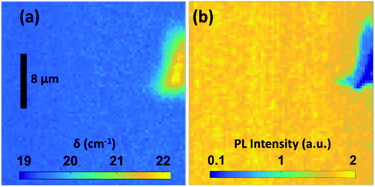 | ||
| Fig. 4 Spatial map of Raman peak distance (a) and PL (b) recorded on a MoS2 sample prepared at 950 °C. | ||
In the following, we will discuss our findings on the basis of different reaction and growth mechanisms. MoS2 synthesis from MoO3 is usually considered as a two-step process comprising partial reduction of MoO3 into MoO3−x under a reducing atmosphere, e.g. using H2, at T ∼ 500–600 °C followed by sulfurization, e.g. using S, at T ∼ 850–1000 °C.18,28,35 Studies also suggest that the MoS2 films produced by a direct one-step sulfurization (i.e. without the intermediate step of partial reduction of MoO3 under H2 gas) were of inferior quality in terms of electrical properties.18 In the present work, the H2S gas, used as a sulfur source, has the beneficial side effect to further reduce the oxidation state of the evaporated MoO3−x films. The processing was performed in the range of the decomposition temperature of H2S, so that a mixture of H2, S and H2S (abbreviated as H2S/S) is expected to be present in the chamber (at T = 650 °C the total conversion of H2S to H2 and S is about 10%![[thin space (1/6-em)]](https://www.rsc.org/images/entities/char_2009.gif) 36,37).
36,37).
Furthermore, at the employed process temperatures (T ≥ 650 °C), MoO3 is considered to evaporate.38,39 In agreement with this physical picture, longer waiting times before H2S injection, i.e. going from process-a to -b and -c, and temperatures above 650 °C (cf. Fig. 1 and 2) result in thinner MoS2 layers due to intermediate evaporation. We note that for the chosen temperature ramp and a process at 750 °C (Fig. 2, blue data), the sample already was at a temperature above 650 °C for 33–43 s at the time of H2S injection, so that significant MoO3−x evaporation is expected before the reaction initiates. MoO3−x atomic layers directly bonded to the substrate may show a higher evaporation temperature as compared with MoO3−x bulk material, resulting in a self-limiting evaporation similar as in atomic layer deposition approaches.
This statement indeed raises a further question: does the evaporated MoO3−x get lost from the process environment or does it play a role in the further film formation by acting as a vapor phase precursor for the synthesis of MoS2? To address this crucial question, we placed a small piece of substrate, which was coated with the MoO3−x precursor in face-up orientation on a blank substrate. We conducted the experiment as process-b sequence at various temperatures and found a clear MoS2 Raman signal on the previously blank substrate in the region adjacent to the precursor covered substrate. This outcome clearly confirms the presence of a CVD like vapor phase transport or reaction mechanism involving MoO3−x vapor and H2S/S. This experiment was repeated on a silicon substrate (at a susceptor temperature of 850 °C) with a 280 nm SiO2 coating, which is known to have better optical contrast for visualization of MoS2.40 Fig. 5(a) and (b) show the optical image of the previously blank substrate after the process and the placement of the precursor containing substrate on top of the larger blank substrate, respectively. Blue regions visible in Fig. 5(a) correspond to areas in which a clear MoS2 Raman signal is observed.
 | ||
| Fig. 5 (a) Contrast-enhanced optical image of the MoS2 film coated on the SiO2/Si substrate, indicating significant contributions from a vapor-phase assisted reaction pathway; arrow indicates the measurement region of the Raman spectrum shown in inset; (b) arrangement of the MoO3−x-coated substrate on the blank substrate. The red box represents the region shown in (a). | ||
Summarizing the discussion above, including the reaction sequence yielding MoS2, the evaporation of MoO3−x, the observed vapor phase reaction for MoS2 deposition, and the possible reaction pathways reported in literature,35,38 we can state that the presented process involve the following reaction mechanisms:
(a) Reaction of solid MoO3−x layers with H2S/S to form MoS2 layer (reaction pathway-1).
(b) Reaction of vapor phase MoO3−x with H2S/S to form MoS2, which adsorbs and grows on the substrate (reaction pathway-2).
(c) Re-adsorption and diffusion of vapor phase MoO3−x on the substrate and reaction in the solid phase with H2S/S to form the MoS2 on the substrate (reaction pathway-3).
Despite the general possibility of all these reaction pathways taking place at the same time, we can discern different probabilities for these routes for different process parameters. In case of process-a (see Fig. 1), when H2S is available from the beginning of the process, the reaction of MoO3−x with H2S can start already even at T < 400 °C,41 which is significantly below the evaporation temperature of MoO3−x. Therefore, all samples prepared up to 650 °C can be considered to follow mainly reaction pathway-1. Even at 700 °C, for which the evaporation temperature of MoO3−x is just crossed, the sample would also predominantly react through reaction pathway-1, i.e. with sulfurization occurring before significant evaporation.
This is drastically changed in case of process-b and process-c, since the H2S gas was not injected before reaching the desired process temperature, so that a noticeable amount of MoO3−x would be already evaporated. This drives the reaction type from pathway-1 towards pathway-2 and -3, especially for higher temperatures and/or later injection times. In accordance to this description we do not see a noticeable difference between process-b and -c for the 0.6 nm sample for the process temperature of 650 °C, which both give a δ value of about 22 cm−1. Here the main reaction takes place most likely via pathway-1.
In case of 700 °C susceptor temperature and process-b or process-c the reaction was accordingly pushed further towards pathway-2 and pathway-3, assumingly still keeping a fraction of pathway-1 in the process. Already at 0 s injection delay (process-b) a significant amount of MoO3−x is evaporated to result in a δ value in the range of monolayer (even if PL did not confirm this clearly, see above). An injection delay of 10 s (process-c) resulted in a clear monolayer signal both from Raman and PL, as the process was pushed further towards pathway-2 and -3 and away from pathway-1. For the discussed results at 750 °C and above the same arguments are valid, leading to a stronger fraction of pathways-2 and 3 compared to pathway-1. It is important to note that higher temperatures, longer H2S injection delays, and different pressure conditions can lead to an escape of the precursor vapour from the vicinity of the substrate surface, preventing the formation of MoS2 layers.
It is expected that pathway-2 and -3 result in a more homogeneous distribution of MoS2 on the substrate, compared to pathway-1. In case of pathway-1, the homogeneity and thickness of MoS2 is directly influenced by the corresponding properties of the MoO3−x precursor layer. For pathways-2 and -3, a rather homogeneous distribution of the reactants occurs through the vapor phase, leading to MoS2 film quality largely independent from the initial MoO3−x film morphology.
An interesting aspect for future works concerns the nanoscale morphology of the prepared monolayers. Although we could demonstrate homogeneous optical properties on length scales from about 1 μm up to several millimeters, the films are expected to be poly-crystalline due to the nature of the growth process. A detailed investigation of nanoscale inhomogeneities, including grain size distributions, grain orientations, grain boundaries as well as possible amorphous regions, may provide further insights and a further understanding of the growth process and potential optimization strategies for tunable optoelectronic properties.
Conclusion
In conclusion, we have demonstrated an approach to synthesize MoS2 thin layers by sulfurization of thermally evaporated MoO3−x precursor layers. Raman and PL spectroscopy confirmed the formation of MoS2 monolayers above a temperature of 700 °C on Si substrates with native oxide and on 100 nm SiO2/Si substrates. We have further investigated possible variations in the process sequence and their influence on the possible reaction pathways for MoS2 film formation. Our study reveals that, in addition to the process temperature, the delay time for the H2S injection is a crucial kinetic parameter, which determines the extent of evaporation of the MoO3−x precursor. This ultimately governs the reaction path (solid or vapor phase reaction) and thickness of the resulting MoS2 layers. The as-grown monolayer samples which were processed in the temperature range of 950–1000 °C exhibit a PL yield on the same quantitative level as exfoliated monolayer flakes.Conflicts of interest
There are no conflicts to declare.Acknowledgements
L. G. and D. P. gratefully acknowledge the funding from German Ministry of Education and Science (BMBF), Grant No.: 03SF0530A. M. A. G. gratefully acknowledges a scholarship by the Consejo Nacional de Ciencia y Tecnología (CONACyT) and the German Academic Exchange Service (DAAD). Partial funding was provided by the Volkswagen foundation through the Lichtenberg professorship “Ultrafast nanoscale dynamics probed by time-resolved electron imaging”.References
- K. F. Mak, C. Lee, J. Hone, J. Shan and T. F. Heinz, Phys. Rev. Lett., 2010, 105, 136805 CrossRef.
- B. Radisavljevic, A. Radenovic, J. Brivio, V. Giacometti and A. Kis, Nat. Nanotechnol., 2011, 6, 147–150 CrossRef CAS.
- A. Ayari, E. Cobas, O. Ogundadegbe and M. S. Fuhrer, J. Appl. Phys., 2007, 101, 014507 CrossRef.
- J. Zhao, W. Chen, J. Meng, H. Yu, M. Liao, J. Zhu, R. Yang, D. Shi and G. Zhang, Adv. Electron. Mater., 2016, 2, 1500379 CrossRef.
- M. Choi, Y. J. Park, B. K. Sharma, S.-R. Bae, S. Y. Kim and J.-H. Ahn, Sci. Adv., 2018, 4, eaas8721 CrossRef PubMed.
- J. Jeon, S. K. Jang, S. M. Jeon, G. Yoo, Y. H. Jang, J.-H. Park and S. Lee, Nanoscale, 2015, 7, 1688–1695 RSC.
- J. Mann, D. Sun, Q. Ma, J. R. Chen, E. Preciado, T. Ohta, B. Diaconescu, K. Yamaguchi, T. Tran, M. Wurch, K. Magnone, T. F. Heinz, G. L. Kellogg, R. Kawakami and L. Bartels, Eur. Phys. J. B, 2013, 86, 2–5 CrossRef.
- J. Robertson, X. Liu, C. Yue, M. Escarra and J. Wei, 2D Mater., 2017, 4, 045007 CrossRef.
- B. Chen, Q. Yu, Q. Yang, P. Bao, W. Zhang, L. Lou, W. Zhu and G. Wang, RSC Adv., 2016, 6, 50306–50314 RSC.
- Y.-H. Lee, X.-Q. Zhang, W. Zhang, M.-T. Chang, C.-T. Lin, K.-D. Chang, Y.-C. Yu, J. T.-W. Wang, C.-S. Chang, L.-J. Li and T.-W. Lin, Adv. Mater., 2012, 24, 2320–2325 CrossRef CAS PubMed.
- K. Kang, S. Xie, L. Huang, Y. Han, P. Y. Huang, K. F. Mak, C.-J. Kim, D. Muller and J. Park, Nature, 2015, 520, 656–660 CrossRef CAS.
- S. Cwik, D. Mitoraj, O. Mendoza Reyes, D. Rogalla, D. Peeters, J. Kim, H. M. Schütz, C. Bock, R. Beranek and A. Devi, Adv. Mater. Interfaces, 2018, 5, 1800140 CrossRef.
- Y. Kim, J. G. Song, Y. J. Park, G. H. Ryu, S. J. Lee, J. S. Kim, P. J. Jeon, C. W. Lee, W. J. Woo, T. Choi, H. Jung, H. B. R. Lee, J. M. Myoung, S. Im, Z. Lee, J. H. Ahn, J. Park and H. Kim, Sci. Rep., 2016, 6, 1–8 CrossRef.
- B. D. Keller, A. Bertuch, J. Provine, G. Sundaram, N. Ferralis and J. C. Grossman, Chem. Mater., 2017, 29, 2024–2032 CrossRef CAS.
- D. Dumcenco, D. Ovchinnikov, K. Marinov, P. Lazić, M. Gibertini, N. Marzari, O. L. Sanchez, Y. C. Kung, D. Krasnozhon, M. W. Chen, S. Bertolazzi, P. Gillet, A. Fontcuberta I Morral, A. Radenovic and A. Kis, ACS Nano, 2015, 9, 4611–4620 CrossRef CAS.
- Y. Kim, H. Bark, G. H. Ryu, Z. Lee and C. Lee, J. Phys.: Condens. Matter, 2016, 28, 184002 CrossRef PubMed.
- H. Liu, K. K. Ansah Antwi, J. Ying, S. Chua and D. Chi, Nanotechnology, 2014, 25, 405702 CrossRef.
- Y.-C. Lin, W. Zhang, J.-K. Huang, K.-K. Liu, Y.-H. Lee, C.-T. Liang, C.-W. Chu and L.-J. Li, Nanoscale, 2012, 4, 6637 RSC.
- A. Castellanos-Gomez, M. Buscema, R. Molenaar, V. Singh, L. Janssen, H. S. J. Van Der Zant and G. A. Steele, 2D Mater., 2014, 1, 011002 CrossRef.
- Y. Yu, C. Li, Y. Liu, L. Su, Y. Zhang and L. Cao, Sci. Rep., 2013, 3, 1866 CrossRef PubMed.
- H. Li, Q. Zhang, C. C. R. Yap, B. K. Tay, T. H. T. Edwin, A. Olivier and D. Baillargeat, Adv. Funct. Mater., 2012, 22, 1385–1390 CrossRef CAS.
- Y.-T. Ho, C.-H. Ma, T.-T. Luong, L.-L. Wei, T.-C. Yen, W.-T. Hsu, W.-H. Chang, Y.-C. Chu, Y.-Y. Tu, K. P. Pande and E. Y. Chang, Phys. Status Solidi RRL, 2015, 9, 187–191 CrossRef CAS.
- L. Liang and V. Meunier, Nanoscale, 2014, 6, 5394–5401 RSC.
- Y. Kim, H. Bark, G. H. Ryu, Z. Lee and C. Lee, J. Phys.: Condens. Matter, 2016, 28, 184002 CrossRef PubMed.
- C. Lee, H. Yan, L. Brus, T. Heinz, J. Hone and S. Ryu, ACS Nano, 2010, 4, 2695–2700 CrossRef CAS PubMed.
- A. M. Van Der Zande, P. Y. Huang, D. A. Chenet, T. C. Berkelbach, Y. You, G. H. Lee, T. F. Heinz, D. R. Reichman, D. A. Muller and J. C. Hone, Nat. Mater., 2013, 12, 554–561 CrossRef CAS.
- H.-Y. Liu, U. K. Das and R. W. Birkmire, Langmuir, 2017, 33, 14580–14585 CrossRef CAS PubMed.
- M. Bosi, RSC Adv., 2015, 5, 75500–75518 RSC.
- A. Özden, F. Ay, C. Sevik and N. K. Perkgöz, Jpn. J. Appl. Phys., 2017, 56, 06GG05 CrossRef.
- K. F. Mak, K. He, C. Lee, G. H. Lee, J. Hone, T. F. Heinz and J. Shan, Nat. Mater., 2013, 12, 207–211 CrossRef CAS PubMed.
- Y. Lin, X. Ling, L. Yu, S. Huang, A. L. Hsu, Y. H. Lee, J. Kong, M. S. Dresselhaus and T. Palacios, Nano Lett., 2014, 14, 5569–5576 CrossRef CAS.
- Y. Xie, Z. Wang, Y. Zhan, P. Zhang, R. Wu, T. Jiang, S. Wu, H. Wang, Y. Zhao, T. Nan and X. Ma, Nanotechnology, 2017, 28, 084001 CrossRef.
- F. Fabbri, E. Rotunno, E. Cinquanta, D. Campi, E. Bonnini, D. Kaplan, L. Lazzarini, M. Bernasconi, C. Ferrari, M. Longo, G. Nicotra, A. Molle, V. Swaminathan and G. Salviati, Nat. Commun., 2016, 7, 13044 CrossRef CAS.
- M. K. L. Man, S. Deckoff-Jones, A. Winchester, G. Shi, G. Gupta, A. D. Mohite, S. Kar, E. Kioupakis, S. Talapatra and K. M. Dani, Sci. Rep., 2016, 6, 20890 CrossRef CAS.
- Q. Ji, Y. Zhang, Y. Zhang and Z. Liu, Chem. Soc. Rev., 2015, 44, 2587–2602 RSC.
- V. E. Kaloidas and N. G. Papayannakos, Int. J. Hydrogen Energy, 1987, 12, 403–409 CrossRef CAS.
- A. N. Startsev, O. V. Kruglyakova, Y. A. Chesalov, S. P. Ruzankin, E. A. Kravtsov, T. V. Larina and E. A. Paukshtis, Top. Catal., 2013, 56, 969–980 CrossRef CAS.
- Y. Y. Wen, X. B. Zeng, X. X. Chen, W. Z. Wang, J. Ding and S. E. Xu, in2nd Annual International Conference on Advanced Material Engineering (AME 2016), 2016, pp. 1034–1039 Search PubMed.
- Y. Feldman, E. Wasserman, D. J. Srolovitz and R. Tenne, Science, 1995, 267, 222–225 CrossRef CAS.
- M. M. Benameur, B. Radisavljevic, J. S. Héron, S. Sahoo, H. Berger and A. Kis, Nanotechnology, 2011, 22, 125706 CrossRef CAS PubMed.
- T. Weber, J. C. Muijsers, J. H. M. C. van Wolput, C. P. J. Verhagen and J. W. Niemantsverdriet, J. Phys. Chem., 1996, 100, 14144–14150 CrossRef CAS.
Footnotes |
| † Electronic supplementary information (ESI) available. See DOI: 10.1039/c8ra08626e |
| ‡ Authors contributed equally to this work. |
| § Current Address: Solid State Physics Department, National Research Centre, 12311 Dokki, Giza, Egypt |
| This journal is © The Royal Society of Chemistry 2019 |