DOI:
10.1039/C8RA08494G
(Paper)
RSC Adv., 2019,
9, 6482-6493
Crystal phase content-dependent functionality of dual phase SnO2–WO3 nanocomposite films via cosputtering crystal growth†
Received
14th October 2018
, Accepted 13th February 2019
First published on 22nd February 2019
Abstract
In this study, crystalline SnO2–WO3 nanocomposite thin films were grown through radio-frequency cosputtering of metallic Sn and ceramic WO3 targets. The W content in the SnO2 matrix was varied from 5.4 at% to 12.3 at% by changing the WO3 sputtering power during thin-film growth. Structural analyses showed that increased WO3 phase content in the nanocomposite films reduced the degree of crystallization of the SnO2 matrix. Moreover, the size of the composite films' surface crystallites increased with WO3 phase content, and the large surface crystallites were composed of numerous nanograins. Addition of WO3 crystals to the SnO2 matrix to form a composite film improved its light harvesting ability. The SnO2–WO3 nanocomposite films exhibited improved photodegradation ability for Rhodamine B dyes compared with their individual constituents (i.e., SnO2 and WO3 thin films), which is attributable to the suitable type II band alignment between the SnO2 and WO3. Moreover, an optimal WO3 phase content (W content: 5.4 at%) in the SnO2 matrix substantially enhanced the ethanol gas-sensing response of the SnO2 thin film. This suggested that the heterojunctions at the SnO2/WO3 interface regions in the nanocomposite film considerably affected its ethanol gas-sensing behavior.
Introduction
SnO2 is an n-type semiconductor with a wide bandgap that can be used in numerous applications, such as gas sensor materials and photocatalysts.1–3 A thin-film structure is a commonly used morphology for wide bandgap oxides in various technological applications. SnO2 thin films have been prepared through various methods such as sputtering, chemical solution deposition, spray pyrolysis deposition, and the sol–gel process.1,4–6 Of these methods, sputtering has the potential to synthesize oxide thin films with precise thickness control, tunable crystallinity, and large-area deposition. Sputtering SnO2 thin films is therefore of potential interest for gas sensor and photocatalyst applications. However, improving the gas-sensing and photocatalytic properties of SnO2 thin films to meet the requirements of such practical applications remains highly desirable. Doping impurity atoms into the SnO2 matrix is a commonly used method for enhancing the gas-sensing and photodegradation properties of SnO2 films. For example, Ce-doped SnO2 thin films exhibit a superior ethanol gas-sensing response to that of pure SnO2 thin films.1 Ag-doped SnO2 thin films have been synthesized through spray pyrolysis, demonstrating enhanced H2S gas detection ability compared with that of pure SnO2 thin films.7 Doping impurity atoms into SnO2 lattices affects the crystal defects and surface morphology of SnO2 thin films, thereby changing its gas-sensing ability. Furthermore, Fe- and Ni-co-doped SnO2 sol–gel-derived thin films exhibit enhanced photocatalytic properties for organic dyes. The dopant modifies the optical bandgap of the SnO2 thin film and enhances its light-harvesting and photocatalytic activity. However, research on a composite film structure containing a different phase in the SnO2 matrix to improve gas-sensing and photodegradation properties for organic dyes has been limited. A SnO2-based composite structure combining SnO2 with another phase has been widely used in one-dimensional and sphere/particle morphologies to improve gas-sensing properties and dye photodegradation ability.8,9 However, due to complex synthesis methods, such two-phase structures in thin films have seldom been reported. SnO–SnO2 composite thin films have been shown to possess superior NO2 sensing ability, and the formation of the SnO–SnO2 junctions at the thin-film surface dominates their gas-sensing ability.10 Sol–gel-derived SnO2–TiO2 composite thin films exhibit improved photodegradation ability for methyl orange, with an optimal phase content ratio.11 Therefore, incorporating other oxide phases into the SnO2 matrix to form SnO2-based composite films for enhanced gas-sensing and photodegradation seems promising.
WO3 is also an n-type semiconductor with a wide bandgap of approximately 2.6–3.6 eV that has been used in gas sensor and catalytic materials.12,13 WO3 thin films are usually prepared through sputtering methods.14 The band alignment between SnO2 and WO3 crystals exhibits a type II band heterojunction, and this composite system is reportedly beneficial in reducing the recombination rate of photogenerated carriers in films.15 Additionally, hydrothermally derived WO3–SnO2 composite particles demonstrate superior sensing behavior toward various volatile organic compounds, compared with the constituent counterparts.16 Similarly, hydrothermally derived WO3–SnO2 nanosheet composites exhibit better acetone gas-sensing behavior than their counterparts.17 Developing a SnO2–WO3 two-phase composite film therefore has the potential to enhance gas-sensing responses and organic dye photodegradation abilities. However, several literatures report the synthesis of SnO2–WO3 composite films through thermal evaporation and pulsed laser deposition with a fixed Sn/W composition source.18,19 These are disadvantageous to modulate the relative phase contents in the composite thin film through a one-step process and are not good strategies to find optimal photodegradation and gas-sensing properties of the composite films associated with the phase content-dependent factors. Developing a single composite film with a SnO2–WO3 two-phase structure through a suitable method therefore has the potential to design and enhance gas-sensing responses and organic dye photodegradation abilities. In this study, SnO2–WO3 composite films with various WO3 phase contents were prepared using dual-gun cosputtering. The advantage of the cosputtering method provides in situ modulation of the relative SnO2/WO3 phase contents during the synthesis of a single composite film. By adjusting sputtering power of the target, varying phase contents of the SnO2 and WO3 are designed and obtained in a single composite film. The effects of WO3 phase content in the SnO2 matrix on the microstructures and optical properties of composite films were investigated. The gas-sensing behavior and photodegradation rate of the nanocomposite films were correlated with the WO3 phase content-dependent microstructures and optical properties.
Experiments
SnO2–WO3 composite films with various WO3 crystal contents were fabricated onto the glass and 300 nm-thick SiO2/Si substrates using dual-gun sputtering system. Sn metallic disc and WO3 ceramic disc with a size of 2 inches were used as sputtering targets to prepare SnO2–WO3composite films. During growth of SnO2–WO3 composite films, the DC sputtering power of Sn target was fixed at 20 W; moreover, the radio-frequency (rf) sputtering power of WO3 target varied from 35 to 65 W. The thin-films growth temperature was maintained at 500 °C with an Ar/O2 ratio of 2![[thin space (1/6-em)]](https://www.rsc.org/images/entities/char_2009.gif) :1; the gas pressure during thin-film deposition was fixed at 1.33 Pa. The distance between the target and substrate is fixed at 7 cm. The rotation speed of the sample holder is fixed at 5 rpm. The sputtering duration for the composite films was fixed at 20 min. The sputtering guns are set to an incline angle of 60° over the sample surface.
:1; the gas pressure during thin-film deposition was fixed at 1.33 Pa. The distance between the target and substrate is fixed at 7 cm. The rotation speed of the sample holder is fixed at 5 rpm. The sputtering duration for the composite films was fixed at 20 min. The sputtering guns are set to an incline angle of 60° over the sample surface.
Sample crystal structures were investigated by X-ray diffraction (XRD; Bruker D2 PHASER) using Cu Kα radiation. The surface morphology of various thin films was investigated by scanning electron microscopy (SEM; Hitachi S-4800). The microstructures of the thin-film samples were characterized by high-resolution transmission electron microscopy (HRTEM; JEOL JEM-2100F). The TEM samples are prepared by dual-beam focused ion beam (FIB: FEI Nova NanoLab 200). The sputtering of top Au layer was performed using Cressington 108 sputter coater. The operating current is set as 40 mA and sputtering time is 15 s. The target and substrate distance is 3 cm; the working pressure is 6 × 10⁻² mbar. The absorption spectra of thin-film samples were conducted by ultraviolet-visible spectroscopy (UV-Vis; Jasco V-750). X-ray photoelectron spectroscopy (XPS; PHI 5000 VersaProbe) analysis was used to determine the chemical compositions of various thin-film samples. The contact angle measurements were performed in atmospheric air at room temperature using a commercial contact angle meter with ±1° accuracy (CA; SEO Phoenix 300). To measure gas-sensing properties, the silver paste was coated onto the surface of the thin-film samples to form electrodes for gas-sensing measurements. The gas sensors made from various thin-film samples were placed in a closed vacuum chamber, and various concentrations of ethanol vapor (100, 250, 500, 750, and 1000 ppm) were introduced into the test chamber, using synthetic air as the carrier gas. The gas sensing response of the thin-film sensors to ethanol vapor is defined as the Ra/Rg. Ra is the sensor electrical resistance in the absence of target gas and Rg is that in the target gas. Photodegradation tests were performed by comparing the degradation of aqueous solution of Rhodamine B (RhB; 10−6 M) containing various thin-film samples under solar light irradiation excited from the 100 W Xe arc lamp. The solution volume of RhB is 20 ml and the sample size for photodegradation tests has a fixed coverage area of 1.5 cm × 1.5 cm.
Results and discussion
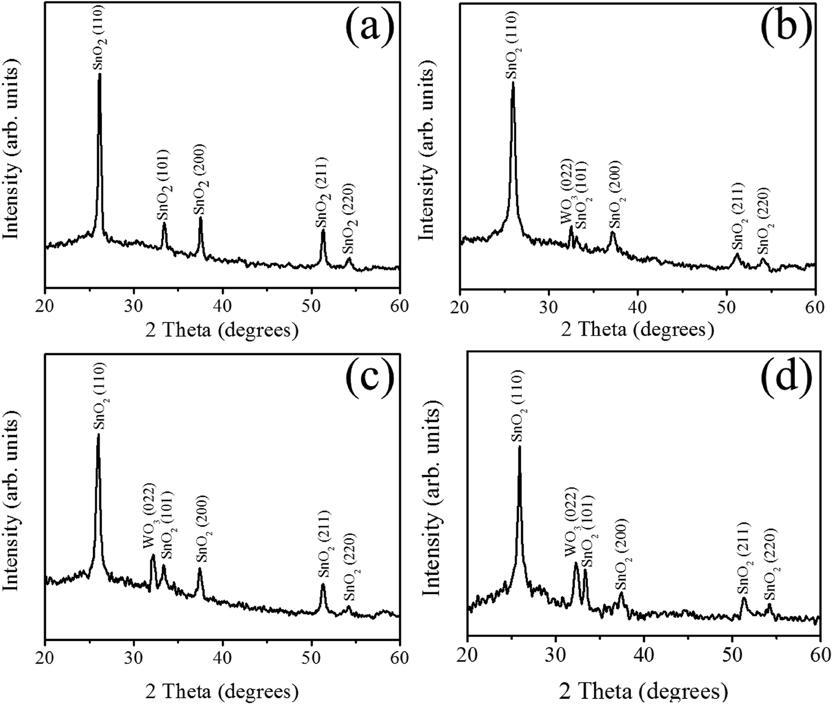
The XRD patterns of SnO2 and composite SnO2–WO3 films prepared under various WO3 sputtering powers are shown in Fig. 1(a)–(d). From Fig. 1(a), the Bragg reflections are ascribed to crystallographic planes of (110), (101), (200), (211) and (220) of tetragonal SnO2 (JCPDS no. 00-002-1337). The sharp and distinct Bragg reflections originated from SnO2 revealed that the as-deposited SnO2 thin film is well crystalline and is in a polycrystalline structure. The SnO2–WO3 composite films grown under various WO3 sputtering powers of 35–65 W exhibited a Bragg reflection centered at approximately 33° and is ascribed to monoclinic WO3 (022) (JCPDS no. 01-089-4476). No other distinct Bragg reflection from impurity phase was observed, indicating that the composite films are composed of SnO2 and WO3 phases. Upon increasing the WO3 sputtering power, the intensity of WO3 (022) peak was gradually increased. Notably, the relative peak intensity of SnO2 (110) is still more intense than that of WO3 (022), showing that the SnO2 is a dominant phase in the composite film. Well crystalline composite films were successfully prepared herein. The crystallite sizes of SnO2 and WO3 are further calculated by using Debye–Scherrer equation.20 The SnO2 film has an average crystallite size of approximately 20 nm. Notably, the average SnO2 and WO3 crystallite sizes decreased during the cosputtering growth of the composite films with an increased sputtering power of WO3. The average SnO2 crystallite size was decreased from 20 in the SnO2 film to 8 nm in the composite film prepared at a WO3 sputtering power of 65 W. Moreover, the WO3 crystallites size in the composite films decreased from 15 to 11 nm when the sputtering power of WO3 was increased from 35 W to 65 W, respectively. The decreased crystallite size of SnO2 and WO3 in the composite films might be associated with the restricted crystal growth of each SnO2 and WO3 crystallites during in situ cosputtering growth of the two-phase structure in the composite film.
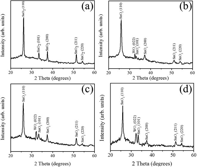 |
| | Fig. 1 (a) XRD pattern of the SnO2 film and XRD patterns of SnO2–WO3 composite films prepared at various WO3 sputtering powers: (b) 35 W, (c) 50 W, (d) 65 W. | |
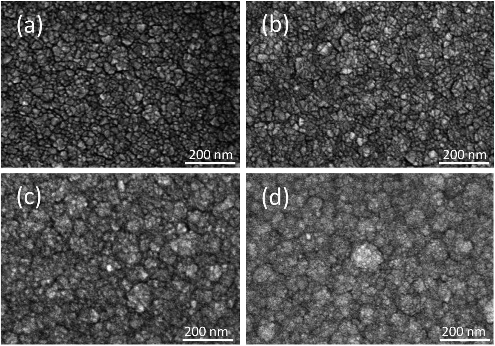
Fig. 2(a)–(d) show SEM micrographs of the surface morphologies of the SnO2 film and SnO2–WO3 composite films grown under various WO3 sputtering powers. In Fig. 2(a)–(d), all the films display a homogenous crack-free appearance. From Fig. 2(a), the surface micrograph of the SnO2 thin film shows the film composed of tiny, irregular crystallites; the film surface had a uniform and dense crystalline form. The surface morphology of the SnO2–WO3 composite film grown under a WO3 sputtering power of 35 W is similar to that of the SnO2 film (Fig. 2(b)); this might be associated with the trace content of WO3 phase in the SnO2–WO3 composite film. Notably, the surface crystallites of the composite films prepared at the higher sputtering powers of WO3 (50 and 65 W) are the clusters composed of crystallites with different sizes. This surface feature is similar to the reported surface structure of the MnO2–WO3 composite films.21 The agglomeration of the nanograins forms large surface clusters and are tightly packed in the composite films with the higher WO3 sputtering power. The surface cluster feature coarsened with an increasing content of WO3 phase in the SnO2–WO3 composite films are clearly demonstrated in the SEM micrographs. The average surface cluster sizes of the SnO2–WO3 composite films prepared at 50 W and 65 W sputtering power of WO3 are 49 and 58 nm, respectively.
 |
| | Fig. 2 (a) SEM image of the SnO2 film. SEM images of SnO2–WO3 composite films prepared at various WO3 sputtering powers: (b) 35 W, (c) 50 W, (d) 65 W. | |
TEM was also used in this study to investigate the microstructures of SnO2–WO3 composite films prepared at the lowest and highest WO3 sputtering powers. Fig. 3(a) shows a low-magnification cross-section TEM image of an SnO2–WO3 composite film grown with a WO3 sputtering power of 35 W, which was composed of distinct columnar grains with diameters of 23–31 nm; no pores were visible on the film surface. Fig. 3(b) displays the selected-area electron diffraction (SAED) pattern from the SnO2–WO3 composite film. The presence of concentric rings that could be indexed to the (110), (200), (211), and (220) planes of tetragonal SnO2 and the (022) plane of monoclinic WO3 revealed that the composite film was of a polycrystalline structure. A high-magnification image of a local region in the SnO2–WO3 composite film is shown in Fig. 3(c); the film had a thickness of approximately 100 nm, and grain boundaries between the columnar grains were visible. High-resolution (HR) TEM images from local regions of the composite film are also displayed in the insets of Fig. 3(c), with ordered and pronounced lattice fringes demonstrating that the composite film was highly crystalline. The long-range distributed lattice spacing of approximately 0.33 nm corresponded to the interplanar spacing of tetragonal SnO2 (110). Moreover, some small regions with ordered lattice fringes had a lattice spacing of approximately 0.27 nm, which corresponded to the interplanar spacing of monoclinic WO3 (022), revealing that SnO2 constituted the major phase in the composite film. Fig. 3(d) shows energy-dispersive X-ray spectroscopy (EDS) spectra obtained from the SnO2–WO3 composite film, verifying that Sn, W, and O were the major elemental components of the sample. The W content in the composite film was estimated at approximately 5.1 at%.
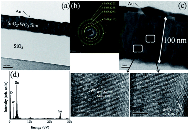 |
| | Fig. 3 TEM analyses of the SnO2–WO3 composite film prepared at the WO3 sputtering power of 35 W: (a) low-magnification TEM image. (b) SAED pattern. (c) High-magnification image. The HRTEM images taken from the local regions of the film are shown in the insets. (d) EDS spectra of Sn, W, and O elements taken from the film. | |
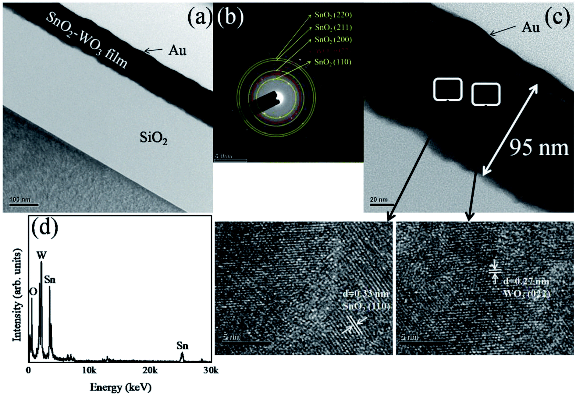
Fig. 4(a) shows a low-magnification cross-section TEM image of the SnO2–WO3 composite film prepared with a WO3 sputtering power of 65 W. The composite film was dense and homogeneously thick throughout the cross-section; the film thickness was approximately 95 nm. Fig. 4(b) shows this composite film's SAED pattern, to which various crystallographic planes of tetragonal SnO2 and monoclinic WO3 (022) were indexed; these crystallographic planes were consistent with the XRD result. The high-magnification TEM image in Fig. 4(c) reveals that the boundary between adjacent columnar grains was less pronounced than that observed in the composite film prepared at a WO3 sputtering power of 35 W, indicating that the major SnO2 crystalline film structure might slightly deteriorate with increasing WO3 phase content in the composite film. HR images from local regions of the composite film exhibit the ordered lattice fringes of tetragonal SnO2 (110) and monoclinic WO3 (022). The EDS spectra in Fig. 4(d) show that the W content of the SnO2–WO3 composite film increased to approximately 12.1 at% at a WO3 sputtering power of 65 W. The W content of composite films prepared at various WO3 sputtering powers was also evaluated using XPS spectra, as illustrated in Table S1 and Fig. S1,† revealing that the composite films' W content evaluated using TEM-EDS was similar to that determined using XPS results.
 |
| | Fig. 4 TEM analyses of the SnO2–WO3 composite film prepared at the WO3 sputtering power of 65 W: (a) low-magnification TEM image. (b) SAED pattern. (c) High-magnification image. The HRTEM images taken from the local regions of the film are shown in the insets. (d) EDS spectra of Sn, W, and O elements taken from the film. | |
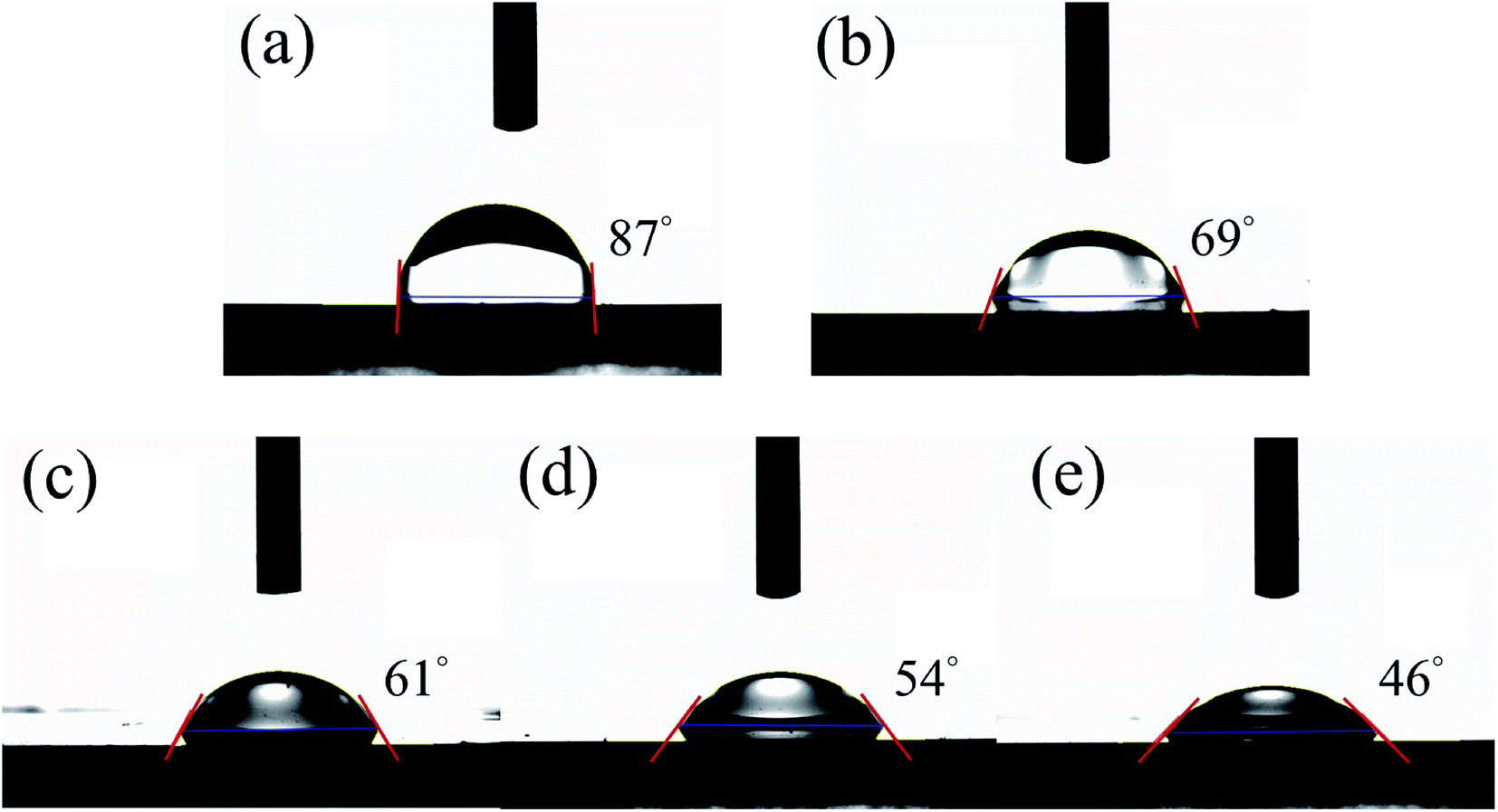
Fig. 5(a)–(e) illustrates changes in the water contact angle on the surface of SnO2, WO3, and composite SnO2–WO3 films with varying WO3 content. Fig. 5(a) shows that the contact angle of the SnO2 thin film was measured at approximately 87°, whereas Fig. 5(b) demonstrates that the WO3 thin film exhibited a contact angle of approximately 69°. The morphology of the solid films could affect their measured contact angle. In this study, the WO3 film was more hydrophilic than the SnO2 film. Incorporation of the WO3 phase into the SnO2 matrix should cause SnO2–WO3 composite films to exhibit a smaller contact angle than that of the pure SnO2 film,22 as shown in Fig. 5(c)–(e). Moreover, the contact angle of the composite film decreased from 61° to 46° as the WO3 sputtering power increased from 35 to 65 W, respectively. Fig. 5(d) and (e) shows that the contact angles were substantially smaller than that of WO3 film. A pronounced surface morphology difference between the WO3 film and the SnO2–WO3 composite films with higher WO3 content, prepared at WO3 sputtering powers of 50 and 65 W, might account for this result. A nanograin agglomeration forming large surface clusters was observed on the SnO2–WO3 composite films with high WO3 sputtering powers (50 and 65 W), which differed considerably from the surface of the WO3 film. The numerous nanograins on the surface clusters of the composite films enhanced their ability to retain absorbed water, resulting in increased hydroxyl content of these films. The nanocomposite films prepared at WO3 sputtering powers of 50 and 65 W thus exhibited increased hydrophilicity compared with the pure WO3 film. A similar surface feature-dependent change in hydrophilicity was reported in Ti anodic oxidation formation of TiO2, consistent with the prediction of the Wenzel theoretical model.23
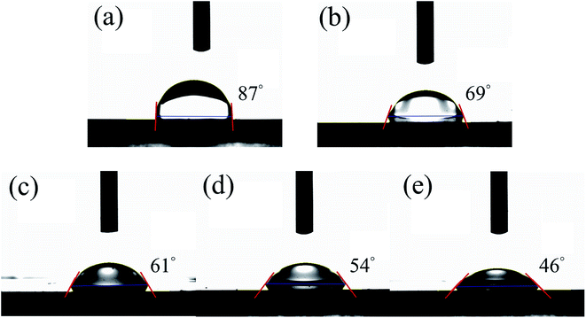 |
| | Fig. 5 (a) and (b) are water contact angle results on the SnO2 and WO3 films, respectively. (c), (d), and (e) are water contact angle results on the SnO2–WO3 composite films prepared at the WO3 sputtering powers of 35, 50, and 65 W, respectively. | |
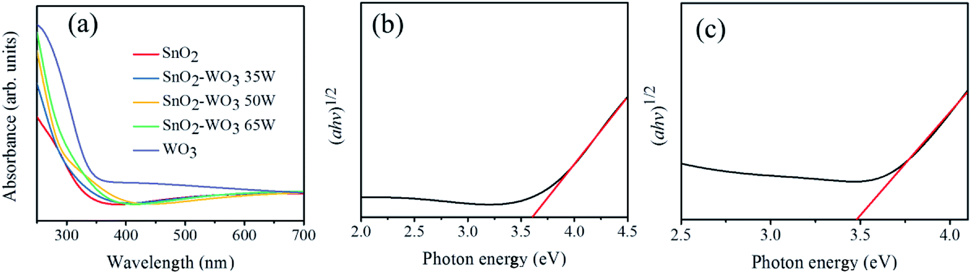
Fig. 6(a) presents a comparison of optical absorbance curves for the SnO2, WO3, and composite SnO2–WO3 films. Because of the wide bandgap energies of SnO2 and WO3 in the UV region, the optical absorbance edges of these films were located in that region. The bandgap values of the synthesized SnO2 and WO3 thin films were evaluated using the Tauc plots in Fig. 6(b) and (c),24 respectively. The SnO2 thin film's bandgap was approximately 3.61 eV, whereas that of the WO3 thin film had a relatively small bandgap of 3.49 eV. Coupling of the SnO2 matrix with the WO3 phase in the composite film might account for the narrower optical bandgap of the composite films, as shown in Fig. 6(a). As the WO3 phase content in the composite thin films increased, a larger degree of redshift in their optical absorbance edge was observed, indicating that the light-harvesting ability of the SnO2 thin film was enhanced by incorporating the WO3 phase.
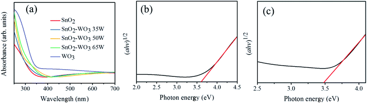 |
| | Fig. 6 (a) UV-Vis absorbance spectra of the SnO2, WO3, and various SnO2–WO3 films. (b) Tauc plot of the SnO2 film. (c) Tauc plot of the WO3 film. | |
Absorbance spectra of the RhB solution after 30, 60, 90, and 120 min of irradiation in the presence of SnO2, WO3, and different composite SnO2–WO3 films are shown in Fig. 7(a)–(d). RhB has a characteristic absorption band at approximately 551 nm. The absorbance spectra intensity of the RhB solution containing various thin-film samples decreased with an increased duration of irradiation. The degradation percentage of RhB absorbance spectra intensity versus the irradiation duration for the RhB solution containing various thin-film samples is shown in Fig. 7(e). Notably, after 120 min, degradation reached approximately 75–90% for the SnO2–WO3 composite films, highlighting their superior photodegradation ability compared with the SnO2 and WO3 films. Moreover, as the WO3 content in SnO2–WO3 composite films increased, the degradation rate significantly improved. The separation efficiency of photoexcited carriers in the SnO2, WO3, and composite SnO2–WO3 films was a key factor affecting the photodegradation rate of these thin-film photocatalysts. Formation of a type II band alignment between the SnO2 and WO3 contact regions in the composite films enhanced photoexcited carrier separation efficiency relative to the composite film constituents (SnO2 and WO3). This could explain the superior RhB dye photodegradation ability of composite films. A possible mechanism for the improved photodegradation ability of composite films is illustrated in Fig. 8(f). Electrons and holes were generated in both the SnO2 and WO3 phases of composite films under irradiation. According to the bandgap energies, the conduction band (CB) edge potential of WO3 is more negative than that of SnO2.15 Therefore, photogenerated electrons in WO3 would easily transfer to SnO2 before recombination, whereas the holes would move in the opposite direction, namely, from the valence band of SnO2 to WO3, resulting in effective charge separation. The greater number of free carriers in the composites than in individual SnO2 and WO3 thin films increased the degree of surface reaction to RhB dyes in the thin-film samples under irradiation. Oxygen, which can accept electrons and combine with hydrogen, produced H2O on the film surface. The electrons accumulating in the CB of SnO2 could be transferred to the adsorbed oxygen, thus yielding ·O2−, which then further reacted to finally produce the active ·OH radical; moreover, the holes transferred to WO3 oxidized H2O molecules to yield hydroxyl radicals, according to the following reactions:
| | |
·O2− + RhB → H2O + CO2
| (4) |
| | |
·OH + RhB → H2O + CO2
| (5) |
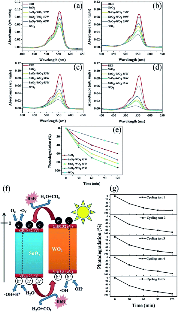 |
| | Fig. 7 The absorbance spectra of the RhB solution containing various thin-film samples under different irradiation durations: (a) 30 min. (b) 60 min. (c) 90 min. (d) 120 min. (e) Percentage photodegradation vs. irradiation duration of the RhB solution containing various thin-film samples. (f) Illustration of photodegradation mechanism for the SnO2–WO3 composite film to RhB dyes. (g) Recycled performances in the presence of the SnO2–WO3 film prepared at 65 W sputtering power of WO3 for photodegrading RhB dyes. | |
 |
| | Fig. 8 Temperature-dependent 100 ppm ethanol gas-sensing responses of the SnO2–WO3 composite film prepared at 35 W sputtering power of WO3. | |
Consequently, ·O2− and ·OH acted as effective oxidants and reacted with RhB on the surface of the SnO2–WO3 composite films. Similar band alignment effects of decreasing the recombination rate of photogenerated carriers have been demonstrated in SnO2–ZnO heterostructured fibers and TiO2–WO3 nanostructures, which improve photodegradation ability toward organic dyes.25,26 The SnO2–WO3 composite film prepared at a WO3 sputtering power of 65 W exhibited the highest degradation ability among the composite film samples, which was attributable to several factors. First, composite film prepared at a WO3 sputtering power of 65 W exhibited a superior hydrophilicity to those prepared at other WO3 sputtering powers. It has been shown that the higher photocatalytic activity exhibited in a TiO2–SnO2 composite film, compared with a pure TiO2 film, was attributable to enhanced hydrophilicity in the composite film.11 Second, a larger degree of redshift of the SnO2 matrix adsorption edge with increased WO3 content was observed. A higher degree of light harvesting and thin film surface hydrophilicity accounted for the superior photodegradation ability of the composite film prepared at a WO3 sputtering power of 65 W. The photodegradation stability of this composite film under irradiation in the RhB solution was evaluated after its recycling (Fig. 7(g)), and after five test cycles it was found to have maintained relatively consistent activity, without apparent deactivation.
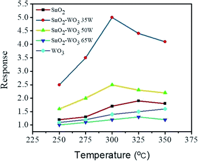
Fig. 8 illustrates the temperature-dependent ethanol gas-sensing response curves of the SnO2, WO3, and composite SnO2–WO3 films on exposure to 100 ppm ethanol. The optimal operating temperature of the semiconductors is associated with a resultant equilibrium between surface reaction with ethanol vapor and the diffusion of ethanol vapor to the surface of the materials.1 An optimal operating temperature of the SnO2 thin film was 325 °C in this study. Furthermore, the highest ethanol gas-sensing response for the WO3 thin film was reached at the operating temperature of 350 °C which is the maximum temperature of the measurement system. The high operating temperature of 350 °C for the WO3 thin film to detect ethanol vapor with a visible response is similar to the previous work.27 Comparatively, the SnO2 thin film is more sensitive to detect ethanol vapor at the relatively lower operating temperature. The higher WO3 phase content in the composite film prepared at the WO3 sputtering power of 65 W deteriorated the performance of the optimal operating temperature and gas-sensing response compared with the SnO2 thin-film matrix. By contrast, the composite films prepared at the WO3 sputtering powers below 50 W exhibited the lower optimal operating temperature at 300 °C. The decreased optimal operating temperature of the composite films prepared at the WO3 sputtering power below 50 W might be associated with the proper potential barrier numbers in the composite films that decreased the optimal operating temperature and also increased the gas-sensing responses in comparison with those of the SnO2 thin film.
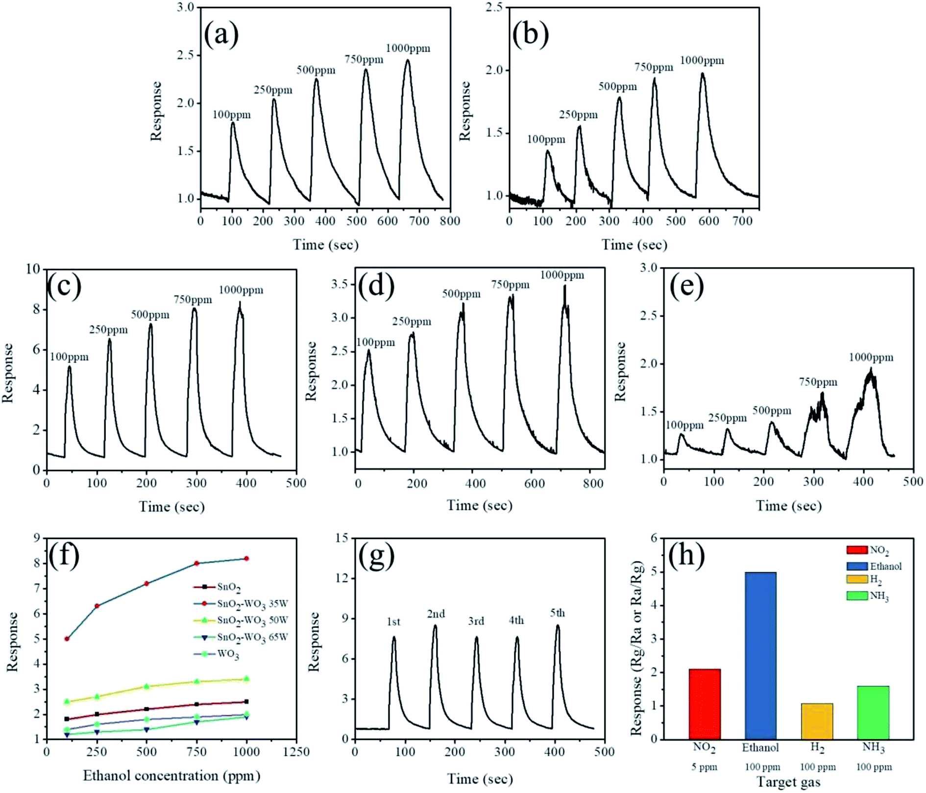
Fig. 9(a)–(e) shows the typical dynamic gas response curves of the SnO2, WO3, and composite SnO2–WO3 films for various concentrations of ethanol vapor (100 to 1000 ppm). The n-type conduction of these oxide films induces oxygen molecules adsorbed on their surface to extract electrons from their CB and became adsorbed oxygen ions on that surface. An electron depletion layer should be formed in the surface region of these films, which increases their electrical resistance. The reaction of ethanol vapor with the adsorbed oxygen ions on n-type oxide films is well documented.1 When reducing gas molecules such as ethanol vapor are introduced on the film surface, the adsorbed oxygen ions release electrons to the film, further reducing its electrical resistance. Fig. 9(a)–(e) shows that the SnO2, WO3, and composite SnO2–WO3 films exhibited a concentration-dependent ethanol gas-sensing response; namely, higher ethanol vapor concentrations resulted in a higher gas-sensing response. This is attributable to the fact that more ethanol molecules react with more adsorbed oxygen ions on the film surface, thus producing a higher gas-sensing response. Moreover, the SnO2, WO3, and composite SnO2–WO3 films demonstrated various degrees of gas-sensing ability to the ethanol vapor, as shown in Fig. 9(a)–(e). The ethanol gas-sensing responses of these films on exposure to various ethanol vapor concentrations are summarized in Fig. 9(f). Notably, the gas-sensing response of the SnO2 film on exposure to 100–1000 ppm ethanol vapor ranged from 1.8 to 2.5, relative to which the WO3 film demonstrated a poorer ethanol gas-sensing ability, with responses ranging from 1.4 to 2.0 when exposed to 100–1000 ppm ethanol vapor. The SnO2–WO3 composite films prepared at a WO3 sputtering power of 35 and 50 W demonstrated enhanced gas-sensing ability compared with their constituent SnO2 and WO3 films. Moreover, the highest ethanol gas-sensing response was observed for the SnO2–WO3 composite film prepared at a WO3 sputtering power of 35 W, attaining gas-sensing responses of 5.1 and 8.3 on exposure to 100 and 1000 ppm of ethanol vapor, respectively. However, as shown in Fig. 9(f), ethanol gas-sensing response rapidly declined when the SnO2–WO3 composite film was prepared at the highest sputtering power of 65 W. This composite film's gas-sensing response was even poorer than that of the individual SnO2 and WO3 films. Comparison of gas-sensing performance demonstrated that a slight increase in WO3 content (preparation at a WO3 sputtering power of 35 W) led to a marked improvement in the SnO2–WO3 composite film's gas-sensing response. Partial addition of a WO3 phase into the SnO2 matrix caused formation of heterojunctions between SnO2 and WO3 crystals. These SnO2–WO3 heterojunctions in turn caused depletion regions to form at heterointerfaces, thereby increasing the number of potential barriers in the composite film. An optimal loading content of ZnO particles in SnO2 tubes was reported to improve gas-sensing responses. This phenomenon is closely associated with modulation of the local depletion layer in SnO2/ZnO contact regions on exposure to target gases.28 Notably, the ethanol gas-sensing response of the SnO2–WO3 composite film prepared at 35 W sputtering power of WO3 on exposure to 20 ppm ethanol (the minimum ethanol concentration in the measurement system) was still visible and the response reached 2.1. Additionally, response and recovery times of the SnO2–WO3 composite films were defined as the durations required for occurrence of a 90% change in resistance on exposure to ethanol gas (response) and air (recovery), respectively. Response times for the SnO2–WO3 composite film prepared at a WO3 sputtering power of 35 W when exposed to various ethanol vapor concentrations (100–1000 ppm) ranged from 6 to 11 s, whereas recovery times ranged from 61 to 71 s. Response times for the composite film prepared at 50 W ranged from 14 to 20 s, whereas those for the composite film prepared at 65 W ranged from 16 to 40 s. Recovery times for the composite films prepared at WO3 sputtering powers of 50 and 65 W all exceeded 80 s. Notably, response times for the SnO2 film were in the range of 11–14 s, and recovery times in the range of 72–153 s. The improved sensing speed of the SnO–WO3 composite film prepared at a WO3 sputtering power of 35 W was thus evident. Fig. 9(g) shows cyclic gas-sensing test results for the composite film prepared at a WO3 sputtering power of 35 W when exposed to 750 ppm of ethanol vapor. Stable sensing behavior over five test cycles was observed for this composite film, demonstrating its high stability and reproducibility for ethanol vapor detection. The gas-sensing selectivity of the film was further investigated on exposure to various oxidizing and reducing target gases in Fig. 9(h). The result demonstrated that the SnO2–WO3 composite thin film was more sensitive to detect ethanol vapor in this study. Table 1 summarizes the ethanol gas-sensing performances of the reported SnO2–WO3 composite film and other SnO2-based composite films prepared using various methods upon exposure to various ethanol vapor concentrations at the sensor operating temperatures of 300 °C.29–31 Comparatively, ethanol gas-sensing responses of the SnO2–WO3 composite film prepared at a WO3 sputtering power of 35 W in this work exhibited a superior gas-sensing response than did those under similar gas-sensing test conditions in previous studies.
 |
| | Fig. 9 (a) and (b) are ethanol gas-sensing response curves of the SnO2 and WO3 films, respectively. (c), (d), and (e) are gas-sensing response curves of the SnO2–WO3 films prepared at WO3 sputtering powers of 35, 50, and 65 W, respectively. (f) Gas-sensing response values vs. ethanol vapor concentrations for various thin films. (g) Cyclic gas-sensing response curves for the SnO2–WO3 film prepared at 35 W sputtering power of WO3 on exposure to 750 ppm ethanol vapor. (h) Gas sensing selectivity histogram of the SnO2–WO3 composite film prepared at 35 W sputtering power of WO3 on exposure to 5 ppm NO2 and 100 ppm of H2 and NH3. | |
Table 1 Ethanol gas-sensing performance of various SnO2–WO3 and other SnO2-based composite films prepared using various methods upon exposure to ethanol vapor at the optimal temperature of 300 °C (ref. 29–31)
| Composite film |
Synthesis method |
Optimal temperature (°C) |
Concentration (ppm) |
Response (Ra/Rg) |
Detection limit (ppm) |
Response/recovery time (sec) |
| SnO2–WO3 |
Hydrothermal method |
300 |
200 |
1.39 |
N/A |
180/200 |
| SnO2–ZnO |
Hydrothermal method |
300 |
200 |
4.5 |
20 |
72/900 |
| SnO2–WO3 (this work) |
Cosputtering |
300 |
250 |
6.5 |
20 |
7/63 |
| SnO2–CeO2 |
Sol–gel method |
300 |
800 |
7.8 |
30 |
60/600 |
| SnO2–WO3 (this work) |
Cosputtering |
300 |
750 |
8 |
20 |
9/67 |
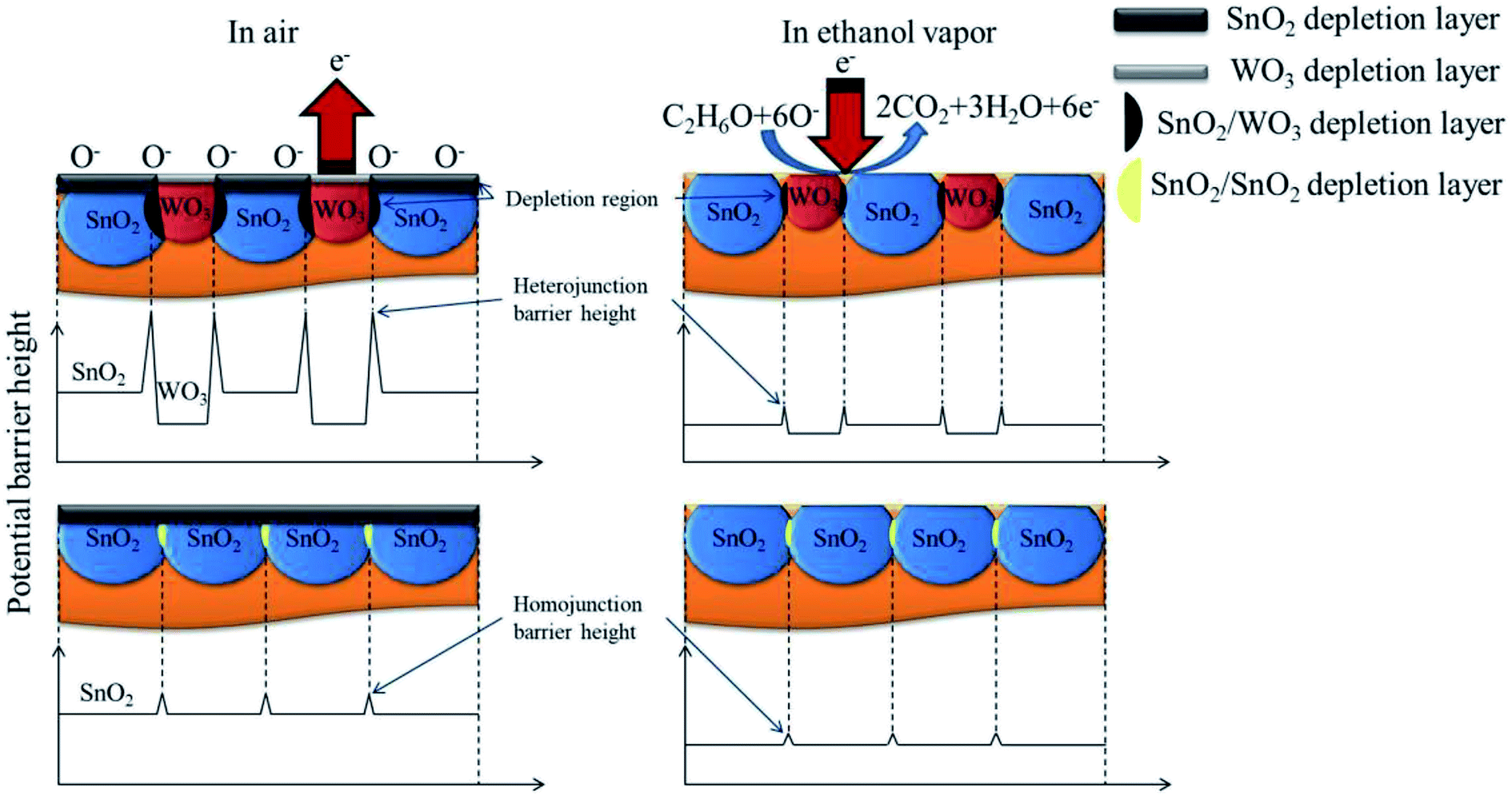
The ethanol gas-sensing mechanisms of pure SnO2 and SnO2–WO3 composites with adequate WO3 phase content in this study are shown in Fig. 10. Surface depletion regions in SnO2 and WO3 crystals and SnO2/WO3 crystal contact regions formed various potential barrier heights. In a gas-sensing test, higher numbers of surface potential barriers may be expected to act with ethanol vapor molecules in the composite film than in the pure SnO2 film. Therefore, a higher degree of resistance variation is observed on exposure to ethanol vapor in the SnO2–WO3 composite film with adequate WO3 phase content. Higher ethanol gas-sensing responses were observed for this composite film than for the pure SnO2 film in given gas-sensing test conditions.
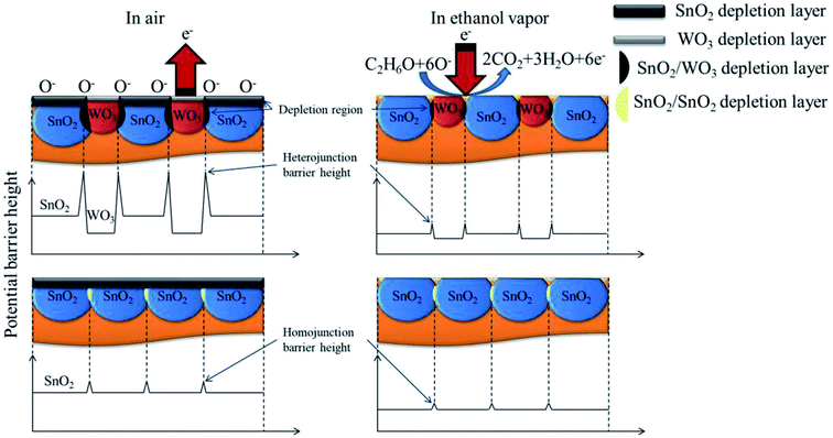 |
| | Fig. 10 Schematics of ethanol gas-sensing mechanisms for the SnO2 and SnO2–WO3 films. | |
Conclusions
In this study, SnO2–WO3 nanocomposite films with various WO3 phase contents were prepared by rf cosputtering metallic Sn and ceramic WO3 targets. The W content of the resulting SnO2–WO3 composite films was varied from 5.4 at% to 12.3 at% through different WO3 sputtering powers. Structural analysis indicated that high WO3 phase content degraded the SnO2 matrix's crystalline quality in the composite films, with surface crystallites in these films becoming coarser. Moreover, a higher light harvesting ability of the composite films was observed with higher WO3 phase content. The SnO2–WO3 composite films exhibited superior RhB dye photodegradation ability relative to their constituents. Ethanol gas-sensing tests revealed that the addition of suitable WO3 crystals (W content of 5.4 at%) to the SnO2 matrix improved the gas-sensing response. The heterogeneous potential barriers in the composite films play an essential role in their ethanol gas-sensing behavior.
Conflicts of interest
There are no conflicts to declare.
Acknowledgements
This work is supported by the Ministry of Science and Technology of Taiwan (MOST 105-2628-E-019-001-MY3).
References
- Y. C. Liang, C. M. Lee and Y. J. Lo, RSC Adv., 2017, 7, 4724–4734 RSC.
- D. Hanft, M. Bektas and R. Moos, Materials, 2018, 11, 1342 CrossRef PubMed.
- A. Bhattacharjee and Md. Ahmaruzzaman, RSC Adv., 2015, 5, 66122–66133 RSC.
- A. Zarkov, A. Stanulis, L. Mikoliunaite, A. Salak and A. Kareiva, Thin Solid Films, 2018, 649, 219–224 CrossRef CAS.
- S. Ben Ameur, H. Belhadjltaief, A. Barhoumi, B. Duponchel, G. Leroy, M. Amlouk and H. Guermazi, Vacuum, 2018, 155, 546–552 CrossRef CAS.
- Talinungsang, D. D. Purkayastha and M. G. Krishna, Appl. Surf. Sci., 2018, 447, 724–731 CrossRef CAS.
- P. S. Kolhe, P. M. Koinkar, N. Maiti and K. M. Sonawane, Phys. B, 2017, 524, 90–96 CrossRef CAS.
- Y. C. Liang and Y. J. Lo, RSC Adv., 2017, 7, 29428–29439 RSC.
- K. Suematsu, N. Ma, M. Yuasa, T. Kida and K. Shimanoe, RSC Adv., 2015, 5, 86347–86354 RSC.
- H. S. Jeong, M. J. Park, S. Kwon, H. J. Joo, S. H. Song and H. I. Kwon, Ceram. Int., 2018, 44, 17283–17289 CrossRef CAS.
- Q. Liu, X. Wu and B. Wang, Mater. Res. Bull., 2002, 37, 2255–2262 CrossRef CAS.
- G. Xie, J. Yu, X. Chen and Y. Jiang, Sens. Actuators, B, 2007, 123, 909–914 CrossRef CAS.
- P. Dong, B. Yang, C. Liu, F. Xu, X. Xi, G. Hou and R. Shao, RSC Adv., 2017, 7, 947–956 RSC.
- D. Valerini, S. Hernández, F. Di Benedetto, N. Russo, G. Saracco and A. Rizzo, Mater. Sci. Semicond. Process., 2016, 42, 150–154 CrossRef CAS.
- J. H. Baek, B. J. Kim, G. S. Han, S. W. Hwang, D. R. Kim, I. S. Cho and H. S. Jung, ACS Appl. Mater. Interfaces, 2017, 9, 1479–1487 CrossRef CAS PubMed.
- A. K. Nayak, R. Ghosh, S. Santra, P. K. Guha and D. Pradhan, Nanoscale, 2015, 7, 12460–12473 RSC.
- M. Yin, Y. Yao, H. Fan and S. Liu, J. Alloys Compd., 2018, 736, 322–331 CrossRef CAS.
- H. Abdul-Ameer, M. AL-Hilli and M. Khalaf, Baghdad Sci. J., 2018, 15, 227–233 Search PubMed.
- A. A. Najim, S. S. Shaker and M. A. H. Muhi, Plasmonics, 2017, 12, 1051–1055 CrossRef CAS.
- V. Madhavi, P. Kondaiah, O. M. Hussain and S. Uthanna, Phys. B, 2014, 454, 141–147 CrossRef CAS.
- C. Zhang, A. Boudiba, C. Navio, M.-G. Olivier, R. Snyders and M. Debliquy, Sens. Actuators, B, 2012, 161, 914–922 CrossRef CAS.
- N. Naseri, R. Azimirad, O. Akhavan and A. Z. Moshfegh, J. Phys. D: Appl. Phys., 2007, 40, 2089–2095 CrossRef CAS.
- B. Li, J. Li, C. Liang, H. Li, L. Guo, S. Liu and H. Wang, Rare Met. Mater. Eng., 2016, 45, 858–862 CrossRef.
- Y. C. Liang and C. M. Lee, J. Appl. Phys., 2016, 120, 135306 CrossRef.
- X. Chen, F. Zhang, Q. Wang, X. Han, X. Li, J. Liu, H. Lin and F. Qu, Dalton Trans., 2015, 44, 3034–3042 RSC.
- B. Lu, X. Li, T. Wang, E. Xie and Z. Xu, J. Mater. Chem. A, 2013, 1, 3900–3906 RSC.
- S. Roy, A. Dey, B. Biswas and S. K. Sarkar, J. Mater. Eng. Perform., 2018, 27, 2635–2642 CrossRef CAS.
- K. Diao, Y. Huang, M. Zhou, J. Zhang, Y. Tang, S. Wang, T. Liu and X. Cui, RSC Adv., 2016, 6, 28419–28427 RSC.
- S. J. Kim, P. Cho, J. H. Lee, C. Y. Kang, J. S. Kim and S. J. Yoon, Ceram. Int., 2008, 34, 827–831 CrossRef CAS.
- K. W. Kim, P. S. Cho, S. J. Kim, J. H. Lee, C. Y. Kang, J. S. Kim and S. J. Yoon, Sens. Actuators, B, 2007, 123, 318–324 CrossRef CAS.
- F. Pourfayaz, A. Khodadadi, Y. Mortazavi and S. Mohajerzadeh, Sens. Actuators, B, 2005, 108, 172–176 CrossRef CAS.
Footnote |
| † Electronic supplementary information (ESI) available. See DOI: 10.1039/c8ra08494g |
|
| This journal is © The Royal Society of Chemistry 2019 |
Click here to see how this site uses Cookies. View our privacy policy here. 
 Open Access Article
 This Open Access Article is licensed under a Creative Commons Attribution-Non Commercial 3.0 Unported Licence
 * and
Yu Chao
* and
Yu Chao