DOI:
10.1039/C8RA07717G
(Paper)
RSC Adv., 2019,
9, 16541-16553
Impact of Cu doping on the structural, morphological and optical activity of V2O5 nanorods for photodiode fabrication and their characteristics†
Received
17th September 2018
, Accepted 18th April 2019
First published on 28th May 2019
Abstract
In this paper, we report a wet chemical precipitation method used to synthesize pure and Cu-doped V2O5 nanorods with different doping concentrations (CuxV2O5 where x = 3, 5 or 7 at%), followed by annealing at 600 °C and characterizations using several techniques. Indeed, a growth mechanism explaining the morphological evolution under the experimental conditions is also proposed. The XRD patterns revealed that all of the studied samples consist of a single V2O5 phase and are well crystallized with a preferential orientation towards the (200) direction. The presence of intrinsic defects and internal stresses in the lattice structure of the CuxV2O5 samples has been substantiated by detailed analysis of the XRD. Apart from the doping level, there was an assessment of identical tiny peaks attributed to the formation of a secondary phase of CuO. SEM images confirmed the presence of agglomerated particles on the surface; the coverage increased with Cu doping level. XPS spectral analysis showed that Cu in the V5+ matrix exists mainly in the Cu2+ state on the surface. The appearance of satellite peaks in the Cu 2p spectra, however, provided definitive evidence for the presence of Cu2+ ions in these studied samples as well. Doping-induced PL quenching was observed due to the absorption of energy from defect emission in the V5+ lattice by Cu2+ ions. We have proposed a cost-effective, less complicated but effective way of synthesizing pure and doped samples in colloidal form, deposited by the nebulizer spray technique on p-Si to establish junction diodes with enhanced optoelectronic properties.
1 Introduction
Semiconductor-based photodiodes have attracted considerable research attention for the past few decades and their optoelectronic devices that harvest photon-energy through distinct electronic processes, with ultra-fast response and high responsivity, are of tremendous use to society in numerous applications as well as optical communications, sensing, motion detection, missile warning and biomedical imaging. All of these applications entail very sensitive devices with high rapidity; fast response time and good signal-to-noise ratio are commonly needed characteristics. Currently, light detection in the UV spectral range still uses Si-based optical photodiodes due to their sensitivity to visible and infrared radiation, intrinsically in the UV region. On this basis, narrow bandgap semiconductors, especially Si (1.1 eV), have been commercialized for light detection for a long time. To avoid these disadvantages, wide-bandgap materials (such as diamond, SiC, III-nitrides and wide-bandgap II–VI materials) are under intensive study to improve the responsivity and stability of UV photodiodes, because of their intrinsic visible-blindness. Among these, vanadium pentoxide (V2O5) is a wide direct bandgap material due to its sensitive UV photoresponse in the UV region. In recent years, much effort has been devoted to V2O5, owing to its remarkable and unique optoelectronic properties, non-toxicity, high thermal and chemical stability, ability for use in cruel environments, radiation hardness, eco-friendliness, low cost, availability, etc. It is considered to be one of the most important metal oxide materials due to its exclusive features and because it is an n-type semiconductor. Metal oxides with a d0 electron configuration, such as V2O5, which contain active sites with the ability to adsorb gaseous molecules and catalyze reactions on their surface have gained attention in past years due to their chemical, electronic and catalytic properties and they have found application in many technological fields. Hence, they have emerged as the most likely to be studied, with potential industrial applications.1–4 A number of methods have been implemented for the synthesis of V2O5 nanoparticles, such as hydrothermal methods,5 solvothermal methods,6 thermal decomposition7 and precipitation.8 Among these methods, wet chemical synthesis is promising for its control of chemical components, low cost, low processing temperature, uniform and chemically homogeneous films, high yield and scalable process. Still, the properties of V2O5 can be doped with metal atoms according to the research needs via doping with various metal atoms to suit the specific needs and applications. Metal substitution can induce extreme modifications in the optical, electrical and magnetic properties of V2O5 by varying its electronic structure or enhancing its activity to produce something of real relevance. Among the major essential difficulties to be conquered is how to increase the electrical conductivity and optical properties of metal oxides. Along with these approaches, metal oxides can be alloyed with proper elements to improve their optical, electrical, and magnetic performance. Hence, an extrinsic dopant (Al, Zn, Cu, W, Co and so on) is considered to be one of the most representative dopants and it can serve as a donor in a V2O5 lattice and increase the wide bandgap engineering (i.e. induce defects), which will improve the electrical and optical properties of V2O5.9–13 In order to improve the material properties, Cu is one of the most important common dopants and it shows a good surface morphology even at high doping levels, a moderately minor amount of deep level traps and low memory effects. In the present work, a systematic attempt has been made to synthesize pure and CuxV2O5 nanorods with different dopant concentrations (x = 3, 5 or 7 at%) by the wet chemical method and capping with PVP. The influence of Cu doping on the structural, morphological and electrical properties of the synthesized samples was also investigated. As an easy example and proposition, we present the colloidal forms of pure and n-CuxV2O5 deposited on p-Si substrate to form a p–n junction through the nebulizer spray technique. We planned and fabricated a device whose recognized diode characteristics and performance parameters were investigated through voltage–current measurements. The results indicate the capability of the photoresponse effect to effectively enhance/optimize the performances of silicon-based optoelectronic devices.
2 Experimental details
2.1 Synthesis of pure and Cu doped V2O5 nanorods
Pure and Cu doped V2O5 nanorods were synthesized using a wet chemical route with various dopant concentrations and additives. All of the chemical reagents were of analytical grade (AR) purity and were used directly without any further purification. Ammonium metavanadate [NH4VO3] was used as the vanadium source and copper nitrate [Cu(NO3)2] as a dopant source material. The details of the synthetic procedures for pure V2O5 nanorods are as follows: 4 mmol of ammonium metavanadate was dissolved in 40 mL of deionized water with vigorous stirring at room temperature. Later, 10 mL of concentrated H2O2 (30%) were added into the above precursor solution with continuous stirring for 30 minutes to obtain a homogeneous solution and then the solution developed a dark brown color. Afterward, 0.10 g of polyvinylpyrrolidone k-30 (PVP) was added to the above solution and the mixture was stirred at 40 °C for 1 h. Then, HNO3 was added drop by drop to the above solution to maintain the pH value throughout the synthesis process.14 The reactants were introduced in this order and stirred for a few minutes until the solution turned an orange-yellow color. Later, the obtained yellow precipitates were collected, washed with deionized water and anhydrous ethanol several times and then dried at 60 °C in air for 10 h. Finally, the above products were heated in a muffle furnace at a 5 °C min−1 heating rate under an air atmosphere at 600 °C for 1 h and cooled to room temperature. Similarly, the Cu doped V2O5 nanorods with different dopant concentrations were also synthesized using the same procedure using the doping source materials.
2.2 Characterization techniques
The structural characterization of the studied samples was performed using X-ray diffraction through a Bruker AXS D8 Advance Discover X-ray diffractometer with CuKα radiation (λ = 1.5406 Å). The morphologies and particles sizes of the products were investigated by scanning electron microscopy (JEOL-model JSM-6390 LV), and high-resolution transmission electron microscopy (TECHNAI T20). The chemical composition was analyzed using an energy dispersive X-ray (EDS) spectroscope attached to the SEM instrument. XPS measurements were carried out using an SSX-100 spectrometer equipped with a focused (spot size 600 Å) mono-chromatized Al Kα (anode hν = 1486.6 eV). The photoluminescence spectrum was examined by an instrument from Horiba Jobin Yvon Fluorolog in the range of 185–900 nm. The current–voltage characteristics of the developed diode were examined using a source meter (Keithley 6517 B) in the dark and under illumination by a calibrated solar simulator with an irradiation intensity of 100 mW cm−2.
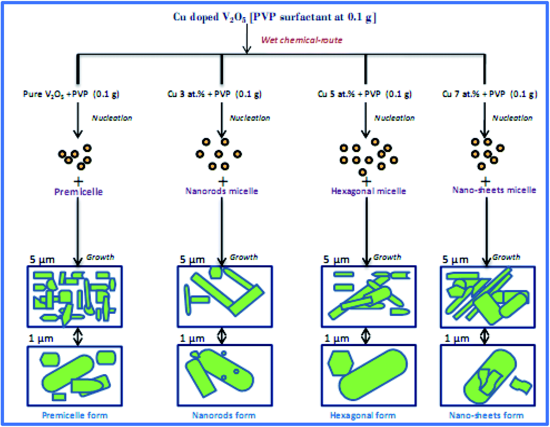
2.3 Possible growth mechanism of the V2O5 nanostructures
The various morphologies of the V2O5 nanostructure formation mechanism were sketched and their schematic representations are shown in Fig. 1. As shown in the figure, the pure V2O5 nanorods assemble into a bundle-like nanorod structure. Previously, Petkov et al.15 presented a new mechanism to explain the processes of V2O5·H2O nanofibers. Recently, Weijie and his co-workers16 have explained the difficulties in the growth of V2O5 nanowires. They also conceived that this mechanism was appropriate for V2O5 nanorods. Therefore, the morphology of V2O5 nanorods can only be due to the effect of the capping agent PVP. In this case, throughout the particle formation, the monomers are adsorbed onto preferred planes and amend the tumor kinetics. Also, in the nucleation stage, growth along all preferred directions might have been retarded to produce a nanorod shaped morphology. Throughout the synthetic process the unbroken [NH4VO3] was precipitated in the natural solution with the concurrent formation of [H2V10O28]4−.17,18 The basic appropriate reactions can be expressed as follows in eqn (1)–(4),19| | |
NH4VO3 + 4H2O2 → NH4[VO(O2)2] + 4H2O + O2
| (1) |
| | |
NH4[VO(O2)2] + H+ → H[VO(O2)2] + NH4+
| (2) |
| | |
10H[VO(O2)2] → [H2V10O28]4− + 4H2O + 9O2
| (3) |
| |
 | (4) |
 |
| | Fig. 1 Schematic diagram of the growth mechanisms of the pure and CuxV2O5 samples. | |
During the reaction time, the [H2V10O28]4− ions gather along the chains which are assembled from the particles of PVP in the synthetic solution. As we know, PVP is a kind of capping agent in which the vinyl groups are hydrophobic while the carbonyl groups are hydrophilic, which is a clue to the formation of chains, which then leads to the formation of micelles. Meanwhile, based on the agglomeration of the ions of [H2V10O28]4− in the solution, the nanorod structure nucleates. At the initial stage of wet chemical treatment in the aqueous H2O2 solution, the chains of PVP form, as revealed above in eqn (3). Alongside these chains, the nanorod structures, which are composed of [H2V10O28]4− ions, start to grow and the novel one-dimensional rod nanostructures are formed. Though the presence of a small quantity of Cu2+ ions on the V2O5 nanorods modifies the growth rate and results in elongated nanorods with a few spherical and microdisk structures. In the synthetic process for Cu doped V2O5, the production of uniform [NH4VO3] was rapid in the initial solution [H2O2] with [Cu(NO3)2], with the simultaneous development of [Cu(OH)2]. This uniform precursor was expected to form a fine powder after heat treatment at 600 °C for 1 h. The basic appropriate reactions can be expressed as follows, eqn (5),
| |
 | (5) |
In the preceding eqn (3), the addition of [Cu(OH)2] ions in the response system changes the kinetics of the growth process, which can be accredited to the fact that the amount of PVP can increase the crystallinity of the studied samples and bring about changes to the morphology, as shown in Fig. 1.
3 Results and discussion
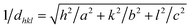
3.1 Structural analysis
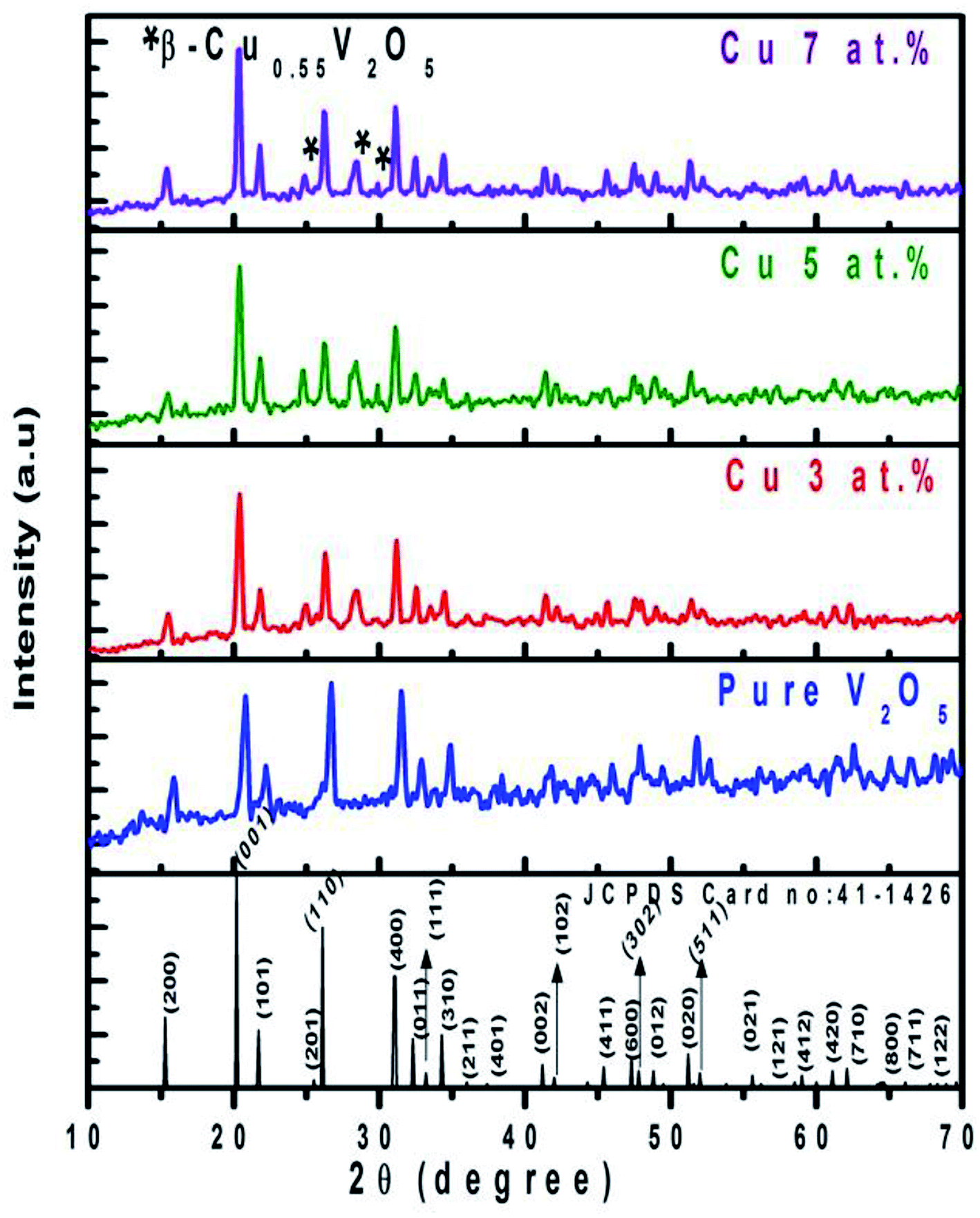
Fig. 2 shows the XRD patterns of pure and CuxV2O5 (where x = 3, 5 or 7 at%) samples annealed at 600 °C. In the figure, the presence of intense diffraction peaks at scattering angles (2θ) of 15.8, 20.7, 21.7, 26.1, 31.4, 32.8, 34.8, and 41.8° are associated with the (200), (001), (101), (110), (400), (011), (310) and (002) planes, respectively.
 |
| | Fig. 2 The XRD patterns of pure and CuxV2O5 (x = 0, 3, 5 or 7 at%) samples annealed at 600 °C for 1 h. | |
All the observed intense peaks can be assigned to the orthorhombic structure of V2O5 with lattice constants of a = 11.51, b = 3.565 and c = 4.4372 Å, according to the reference pattern JCPDS card no. 41-1426. No diffraction peaks from other crystalline impurities can be perceived, indicating that all the studied samples are single phase. In the figure, the presence of a secondary phase is attributed to Cu clusters or vanadium oxides that could be detected in the XRD patterns of the CuxV2O5 samples. The existence of additional peaks at 2θ = 24.86, 28.41 and 30.06° (marked by*) correspond to (202), (401) and (112) planes, respectively. The observed additional peaks can be identified as a monoclinic crystal structure of β-Cu0.55V2O5 with space group Cm(8) whose lattice constants are a = 15.25 Å, b = 3.620 Å and c = 10.100 Å (JCPDS card no. 70-2145).20
Assimilation of a Cu atom strongly affects the growth of the (110) peak and the same enhancement in the growth of the (001) peak due to the introduction of the new Cu phase was observed at 2θ = 24.86, 28.41 and 30.06°, which modifies the preferential orientation from (110) to (001). In the figure, the intensity of the (200) plane decreases with an increase in Cu2+ content up to 5 at% while at a higher doping level it is increased due to the super-saturation of Cu atoms into the V2O5 matrix. The same scenario is also observed for the (110), (400) and (310) planes. This may be due to the augmentation of the (001) and (101) major planes. Also the doping concentration increased the major peak positions in the diffraction patterns and they were shifted to lower 2θ values.
This can be attributed to the higher ionic radii of Cu2+ (0.071 nm) compared to V5+ (0.068 nm). Although, with an increase in the Cu2+ doping content we also intuit that the intensities of the intense diffraction peaks (001) and (101) are gradually increased and that their half height widths are increased, indicating a reduction in grain size with respect to the pure sample. The peaks become sharper at a higher Cu concentration, indicating smaller grain sizes, while the peak intensity increases. The average crystallite sizes of the investigated samples were determined from the XRD pattern using the Debye–Scherrer formula, D = 0.89λ/β![[thin space (1/6-em)]](https://www.rsc.org/images/entities/char_2009.gif) cosθ, where λ is the wavelength of the X-ray radiation, and β is the full width at half-maximum of the peak at diffraction angle θ.21 The estimated average grain sizes are listed in Table 1 and it can be observed that the rise in crystallite size of V2O5 upon substitution is owing to the crystallinity being enriched with cumulative concentration when annealed in an oxygen environment at 600 °C.
cosθ, where λ is the wavelength of the X-ray radiation, and β is the full width at half-maximum of the peak at diffraction angle θ.21 The estimated average grain sizes are listed in Table 1 and it can be observed that the rise in crystallite size of V2O5 upon substitution is owing to the crystallinity being enriched with cumulative concentration when annealed in an oxygen environment at 600 °C.
Table 1 The estimated structural parameters of pure and Cu doped V2O5 samples annealed at 600 °C for 1 h
| CuxV2O5 (where x = 0, 3, 5 or 7%) |
2θ (degree) |
(hkl) crystal system |
d-Spacing (nm) |
FWHM (degree) |
Grain size (D) (nm) |
Lattice parameters (Å) |
Stress σ (Pa) |
Strain (ε) |
Internal parameter “U” |
| JCPDS standard |
JCPDS observed |
a |
c |
| 00 |
15.8303 |
200 |
0.5768 |
0.55937 |
0.48720 |
17.1945 |
11.30 |
4.441 |
3.4238 |
2.4769 |
2.4081 |
| 20.7631 |
001 |
0.4379 |
0.42746 |
0.45970 |
17.5776 |
11.42 |
4.358 |
3.7953 |
2.5138 |
2.5389 |
| 26.6500 |
110 |
0.3408 |
0.33422 |
0.38510 |
21.2100 |
11.44 |
4.316 |
3.9832 |
2.5000 |
2.5918 |
| 03 |
15.4633 |
200 |
0.5768 |
0.57257 |
0.40950 |
20.4481 |
11.47 |
4.358 |
3.7953 |
2.5292 |
2.5590 |
| 20.3748 |
001 |
0.4379 |
0.43552 |
0.36820 |
21.9323 |
11.48 |
4.357 |
3.7998 |
2.5323 |
2.5567 |
| 26.2822 |
110 |
0.3408 |
0.33881 |
0.32790 |
24.8912 |
11.47 |
4.363 |
3.7729 |
2.5292 |
2.5537 |
| 05 |
15.4381 |
200 |
0.5768 |
0.57350 |
0.40260 |
20.7979 |
11.49 |
4.362 |
3.7774 |
2.5353 |
2.5628 |
| 20.3774 |
001 |
0.4379 |
0.43546 |
0.35800 |
22.5573 |
11.48 |
4.364 |
3.7685 |
2.5323 |
2.5567 |
| 26.2304 |
110 |
0.3408 |
0.33947 |
0.34940 |
23.3571 |
11.47 |
4.360 |
3.7864 |
2.5292 |
2.5569 |
| 07 |
15.3891 |
200 |
0.5768 |
0.57531 |
0.38890 |
21.5293 |
11.49 |
4.366 |
3.7595 |
2.5384 |
2.5626 |
| 20.3390 |
001 |
0.4379 |
0.43628 |
0.30940 |
26.0991 |
11.50 |
4.364 |
3.7685 |
2.5384 |
2.5647 |
| 26.2198 |
110 |
0.3408 |
0.33960 |
0.29340 |
27.8145 |
11.51 |
4.363 |
3.7729 |
2.5415 |
2.5698 |
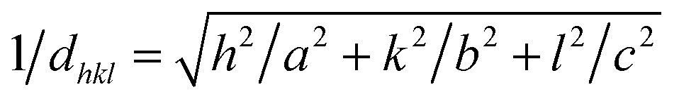
In this regard, the improvement in crystallinity with thermal annealing could be attributed to many factors, such as: removal of defects and internal stresses caused by defects, removal of external stresses arising from the lattice mismatch and grain growth due to the coalescence process.22 The grain growth at a higher annealing temperature is due to the fact that the temperature is high enough to initiate a coalescence process, which improves the crystallinity of the studied samples.23 The lattice parameters a and c are determined using the orthorhombic structural relationship of V2O5, eqn (6),24
| |
 | (6) |
where,
a and
c are the lattice constants;
h,
k and
l are the Miller indices of the plane; and
dhkl is the interplanar
d-spacing. The interplanar
d-spacing can be calculated from Bragg's law.
The estimated lattice parameters are listed in Table 1 and it can be observed that the values of the lattice parameter increase with an increase in the Cu2+ doping concentration. The value of stress in the studied samples is also calculated using the following eqn (7),25
| | |
σ = −233 × 109[C − C0/C0]
| (7) |
where
σ is the stress, “
C” is the lattice parameter of the studied sample and “
C0” is the strain-free lattice parameter (0.5206 nm).
The stress (σ) in the investigated samples can be ascribed to two main causes: an intrinsic stress due to the impurities and defects in crystal and an extrinsic stress due to lattice mismatch, growth conditions and a mismatch in the thermal expansion coefficients of the sample.26 The lattice strain of the samples is calculated using the following expression, eqn (8),27
where
a0 = 0.325 nm is the lattice constant of standard V
2O
5 and “
a” is the lattice constant calculated for the studied sample. The estimated values of lattice strain (
ε) and stress (
σ) values are listed in
Table 1, which shows a comparable deviation from the maximum value of the lattice parameters a and
c. The pure V
2O
5 sample has maximum stress (
σ) and strain (
ε) values, which go on decreasing as we increase the doping concentration. From the stress (
σ), strain (
ε) and their corresponding sign values, we can infer that the studied films are in a compressed state. The reduced values of stress (
σ) and strain (
ε) suggest that the studied samples are becoming relaxed due to a re-adjustment of the lattice at a higher annealing temperature,
i.e. at 600 °C. In
Table 1 we have also calculated internal parameter “
U”, which is the deformation ratio for the polycrystalline symmetry as follows,
eqn (9),
28| |
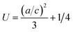 | (9) |
The expected values are found to deviate from the ideal values of (2.4081) to (2.5626) for the pure V2O5 sample (Table 1) and the increase in “U” values indicates an increase in overall lattice distortion.
3.2 SEM–EDS analysis
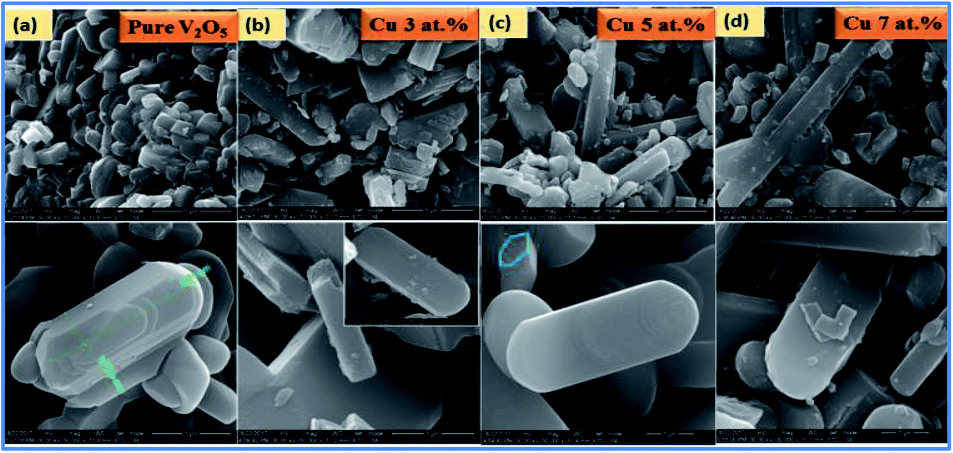
SEM images of pure and Cu doped V2O5 samples (x = 3, 5 or 7 at%) with different dopant levels are shown Fig. 3(a–d).
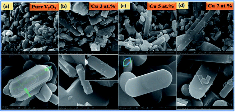 |
| | Fig. 3 SEM images of (a–d) pure and CuxV2O5 samples annealed at 600 °C for 1 h. | |
Fig. 3(a) shows that nanorods with a hexagonal-like face are formed for pure V2O5 and all of the nanorods are long with blunt ends. It is clearly revealed that the synthesized material possesses ultrathin 1-D nanorods structures which are grown in very high density. In the figure, the high magnification SEM image shows that the nanorods are connected with each other and form nanorod networks. Fig. 3(b–d) display the SEM images of CuxV2O5 samples with different dopant concentrations. In this regard, at a lower concentration of CuxV2O5, samples displayed a microdisk with nanorods. At higher concentration, the morphology progressively turned from microdisks to nanodisks, compared to a lower doping concentration.
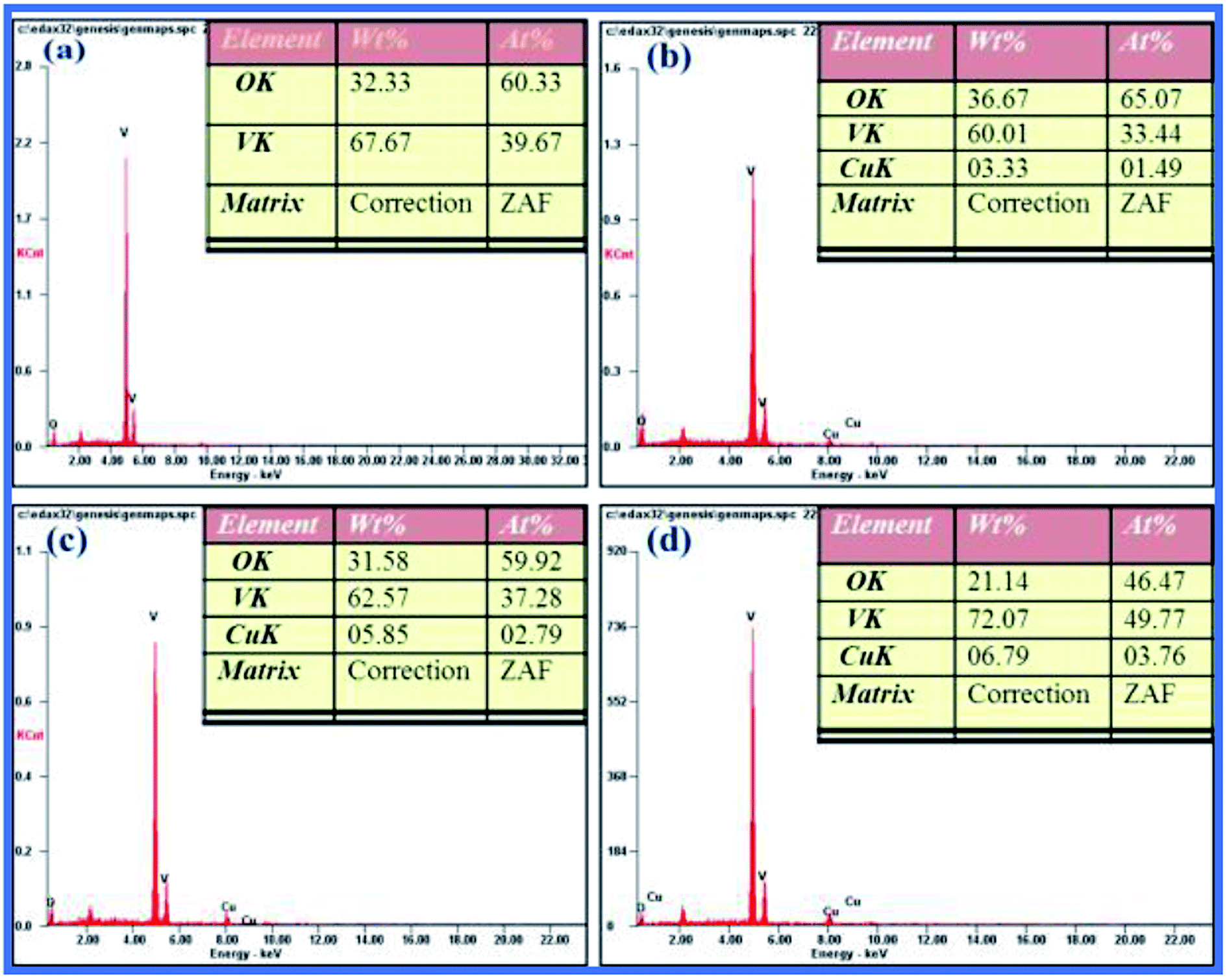
The morphological variation can be credited to the huge influence of Cu2+ ions doped in the V2O5 lattice and their dipolar interaction along the C-axis orientation. A possible reason for the morphological transition of V2O5 from nanorods to nanodisks on Cu doping is the fact that mixing/doping/alloying of specific elements plays a major role in modifying the dimensions of nanostructures.29,30 The elemental composition of the synthesized samples was examined by energy dispersive spectroscopy and their measurements in SEM performed on pure and doped sample growth products reveal a homogeneous distribution of all the elements and confirm the presence of Cu in the doped elements. It is clear from Fig. 4(a–d) that V and O are in the 1:1 atomic% ratio of V2O5, which means they are according to their stoichiometry. The presence of a Cu peak in the EDS spectrum clearly confirmed that the Cu is efficiently doped into the V2O5 nanodisk networks.
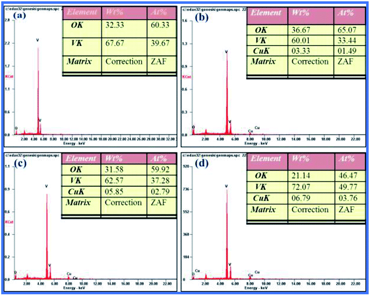 |
| | Fig. 4 EDS spectrum of (a) pure and (b–d) CuxV2O5 samples annealed at 600 °C for 1. | |
3.3 TEM analysis
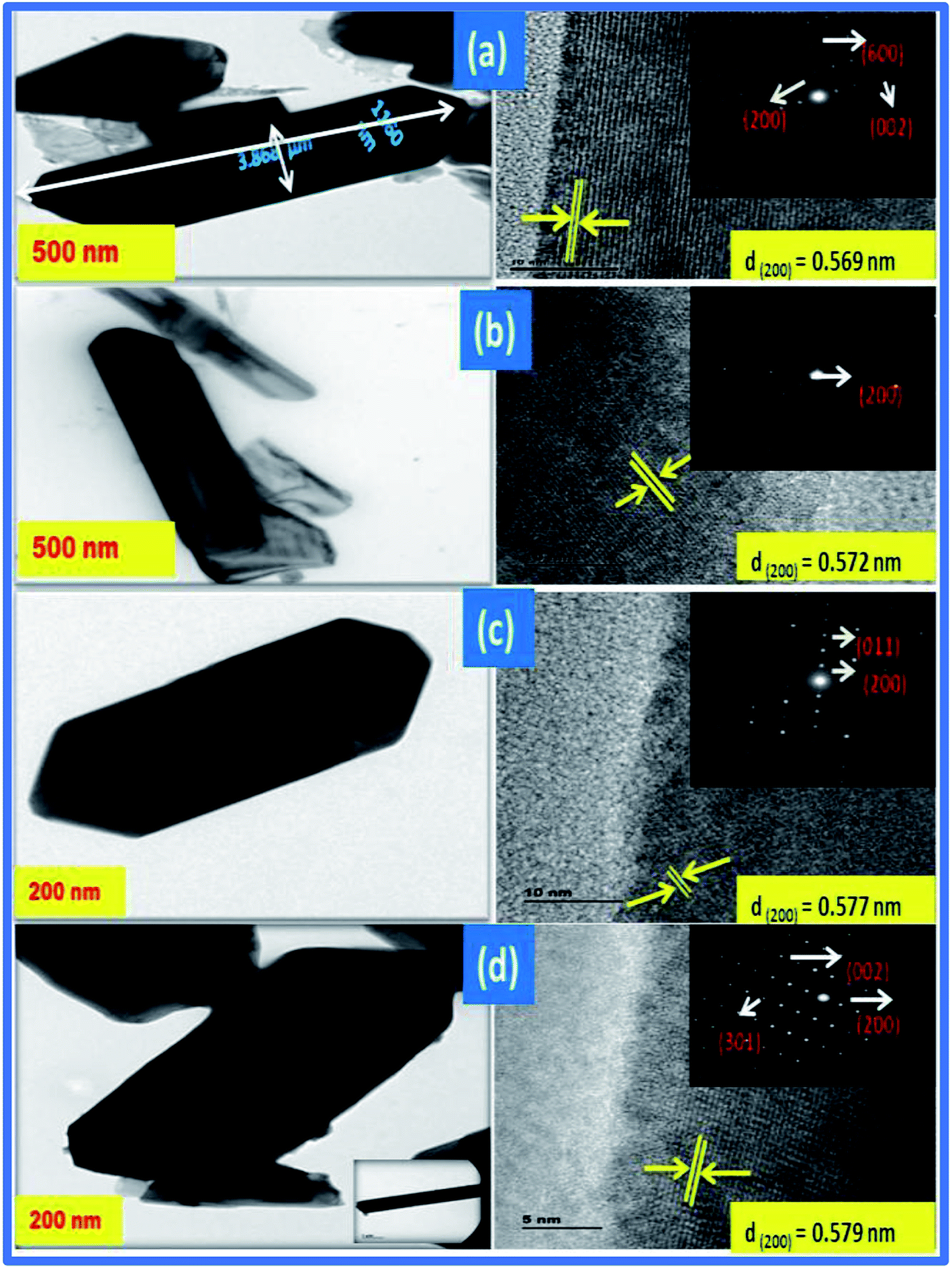
TEM analysis was carried out to investigate the detailed structural characteristics of the studied samples, as shown in Fig. 5(a–d). In the figure, the boundaries of the pure V2O5 nanorods are highlighted in the images for better visualization and individual nanorods are 200–500 nm in width and 1–2 μm in length.
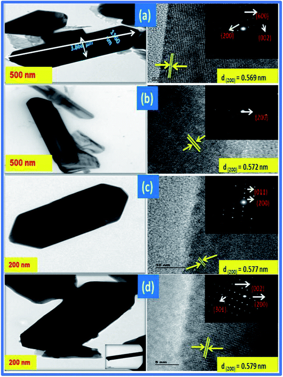 |
| | Fig. 5 TEM images of (a) V2O5 with inset SAED pattern and lattice fringes and (b–d) CuxV2O5 samples with inset SAED patterns and lattice fringes. | |
In addition, the clear lattice fringes with an interplanar d-spacing of ∼0.569 nm agree well with the distances of the (200) lattice planes of the orthorhombic V2O5 phase, and the clear diffraction spots in the SAED pattern (inset in Fig. 5(a)) further revealed that the nanorods are single-crystalline. Fig. 5(b–d) show the Cu doped V2O5 samples containing 3, 5 and 7 at% Cu with a mean diameter ranging from 100 to 200 nm. The disk-like hierarchical structures could also be distinguished from the TEM images by the round shape from the front and the rectangle from the side of the disk. When the doping concentration was further increased, the separated nanosheets merged together and generated a rod-like structure, as shown in Fig. 5(c). At higher concentration, the nanosheet morphology disappeared completely and distinct nanorods (Fig. 5(d)) formed with widths of 200–500 nm and lengths around 1 μm, while the particle size of the sample annealed at 600 °C grew significantly to around 1 μm in width and 2 μm in length with poor homogeneity (Fig. 5(b–d)). The figure clearly shows that the morphology changes from nanorods to nanodisks on Cu2+ doping. The insets to Fig. 5(b–d) show that the lattice d-spacings of the CuxV2O5 samples calculated from the HRTEM images are in the range of 0.572–0.579 nm, which matches well with the lattice spacing of the (001) plane of V2O5. The inset SAED pattern confirms that the prepared nanoparticles have a high degree of crystallinity. The diffraction bright spots correspond to the (200) plane of the orthorhombic phase and can be attributed to the short-range ordering among the unit cells caused by the doping.
3.4 XPS analysis
XPS studies were carried out on pure and CuxV2O5 samples (x = 5 at%) to study the distribution and the chemical oxidation state of vanadium in the sample was investigated, as shown in Fig. 6(a–d). The survey scan spectra of the prepared samples were recorded up to 1350 eV (Fig. 6(a)) and this showed that all peaks could be assigned to vanadium (V), oxygen (O), carbon (C) or copper (Cu), and no other impurities could be observed in the samples. The binding energy 284.16 eV of C 1s is used as a reference in the spectra, as shown in Fig. 6(b). The existence of C in the sample was attributed to carbon tape. Fig. 6(c) shows the narrow scan spectra of the V and O elements in the sample. In the figure, binding energies are around 517.04 and 524.47 eV attributed to V5+ in V2p1/2 and V2p3/2 electronic states, respectively.31 The sharp peak at 524.47 eV is associated with V5+ species present in the sample which are in completely oxidized states. The O 1s spectrum (Fig. 6(c)) exhibits one peak at about 530.94 eV which can be assigned to O2−.32 The O 1s band has two components. The terminal oxygen (![[double bond, length as m-dash]](https://www.rsc.org/images/entities/char_e001.gif) O) and the linkage (–O–) are associated with the O2− state. Further, the high binding energy peaks indicate dissociated oxygen or chemisorbed or OH species on the surface of V5+. The influence of Cu doping studied by the high-resolution Cu 2p doublet spectra of CuxV2O5 (x = 5 at%) is shown in Fig. 6(d), which shows the Cu 2p doublet whose binding energies are 953.873 and 933.771 eV for Cu 2p1/2 and Cu 2p3/2, respectively. The occurrence of weak satellite peaks on the higher binding energy (943.2 and 962.4 eV) side of the Cu 2p main peak also indicates the presence of Cu2+ ions. The +1 and +2 valence of Cu ions show good similarity to previously reported work.33 The splitting of the Cu 2p doublet at 20.1 eV is observed for Cu 2p1/2 and Cu 2p3/2, while it matches well with that of CuO,34,35 which confirms the substitution of Cu ions for vanadium sites in the V5+ lattice.
O) and the linkage (–O–) are associated with the O2− state. Further, the high binding energy peaks indicate dissociated oxygen or chemisorbed or OH species on the surface of V5+. The influence of Cu doping studied by the high-resolution Cu 2p doublet spectra of CuxV2O5 (x = 5 at%) is shown in Fig. 6(d), which shows the Cu 2p doublet whose binding energies are 953.873 and 933.771 eV for Cu 2p1/2 and Cu 2p3/2, respectively. The occurrence of weak satellite peaks on the higher binding energy (943.2 and 962.4 eV) side of the Cu 2p main peak also indicates the presence of Cu2+ ions. The +1 and +2 valence of Cu ions show good similarity to previously reported work.33 The splitting of the Cu 2p doublet at 20.1 eV is observed for Cu 2p1/2 and Cu 2p3/2, while it matches well with that of CuO,34,35 which confirms the substitution of Cu ions for vanadium sites in the V5+ lattice.
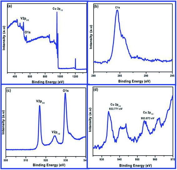 |
| | Fig. 6 XPS spectra of (a) survey scan, (b) C 1s level, (c) V 2p, O 1s and (d) Cu 2p level spectra. | |
3.5 Photoluminescence analysis
The PL spectra of the studied samples recorded at room temperature are shown in Fig. 7. There are three distinct emission bands in the spectra of the V2O5 sample; one peak is in the ultraviolet emission at 418 nm (2.96 eV), there is a strong blue emission at 440 nm (2.81 eV) and broad visible emission at 549.2 nm (2.26 eV). The UV and visible peaks are familiar in the PL spectrum of V2O5.36
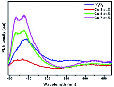 |
| | Fig. 7 PL spectrum of pure and CuxV2O5 samples annealed at 600 °C for 1 h. | |
In this spectrum, a band-emission at 418 nm could be due to defects, such as the interface trap existing at the grain boundaries, and it originates from exciton recombination corresponding to the near-band edge (NBE) exciton emission of the wide bandgap V2O5, that is, free exciton recombination through an exciton collision process. The blue-green emission band centered at 453 nm could be attributed to the radioactive recombination process of a self-trapped exciton ascending from the charge transfer excited state of the V2O5 class. Also they have been attributed to the presence of a high density of surface defects, including oxygen vacancies, vanadium vacancies, oxygen interstitials and vanadium interstitials in the samples. This result suggests electron transition from the level of the ionized oxygen vacancies to the valence band. The broad visible emission peak at 550 nm is due to the recombined emission of the lowest split-off V 3d band to the O 2p valence band.37 Fig. 7 shows the influence of Cu2+ on the PL intensity of the V2O5 samples. It can clearly be noted that the PL intensity decreases with lower Cu2+ substitution compared with pure V2O5. This decrease in the PL intensity may involve several non-radiative recombination processes happening in the present samples.38 A similar result with other materials has been reported by Wang et al.39–41 However, at 5–7% Cu concentration, the PL intensity growth, which specifies the surface to volume ratio, decreases; consequently, surface defects decreased with increasingly higher doping concentration.
3.6 Device fabrication process
In our experiment, a p-type silicon wafer (B-doped (100) wafer, 1–30 Ω cm) was exploited for fabrication of the diode. Before the fabrication, the silicon substrate was ultrasonically cleaned for 5 minutes in acetone, distilled water and ethanol, consecutively. In order to remove the native oxide layer from the surface of the silicon, the wafer was immersed for 1–2 minutes into a buffered/piranha solution of HF (HF:H2O = 1:7). Finally, the wafer was blow dehydrated with nitrogen.42 The systematically cleaned Si substrate was immediately placed on the sample holder of a spray setup. Herein, the sprayed solution was prepared by using 100 mg of the synthesized samples dispersed in 100 mL of 2-propanol under constant stirring for one day. The process was completed by depositing the aqueous solution via the nebulizer spray technique onto a preheated Si (100) substrate at 150 °C. After coating, we obtained a dark yellow color on top of the substrate. Furthermore, an ohmic contact was prepared with a high-purity Ag paste applied to the front and back surfaces of the wafer.
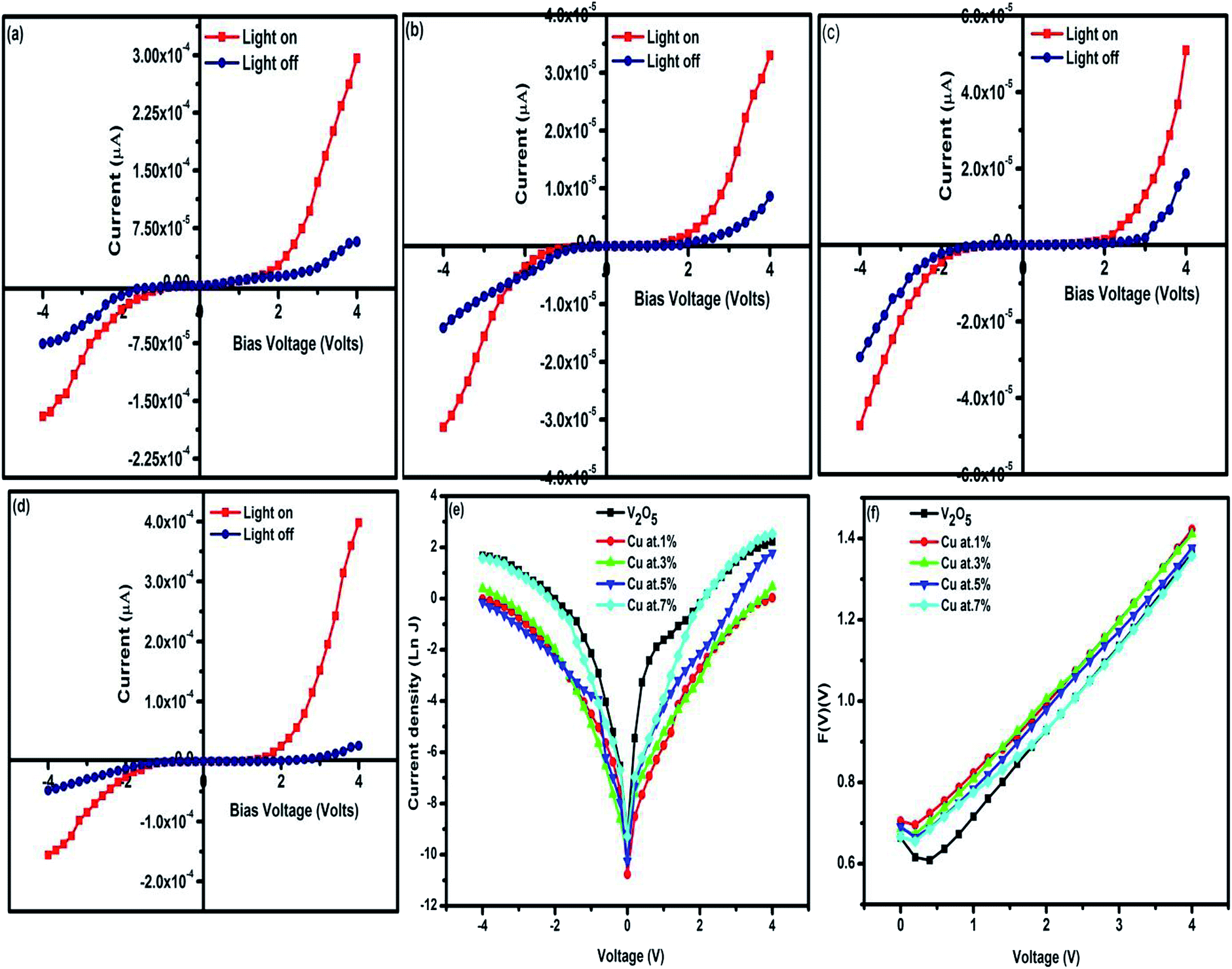
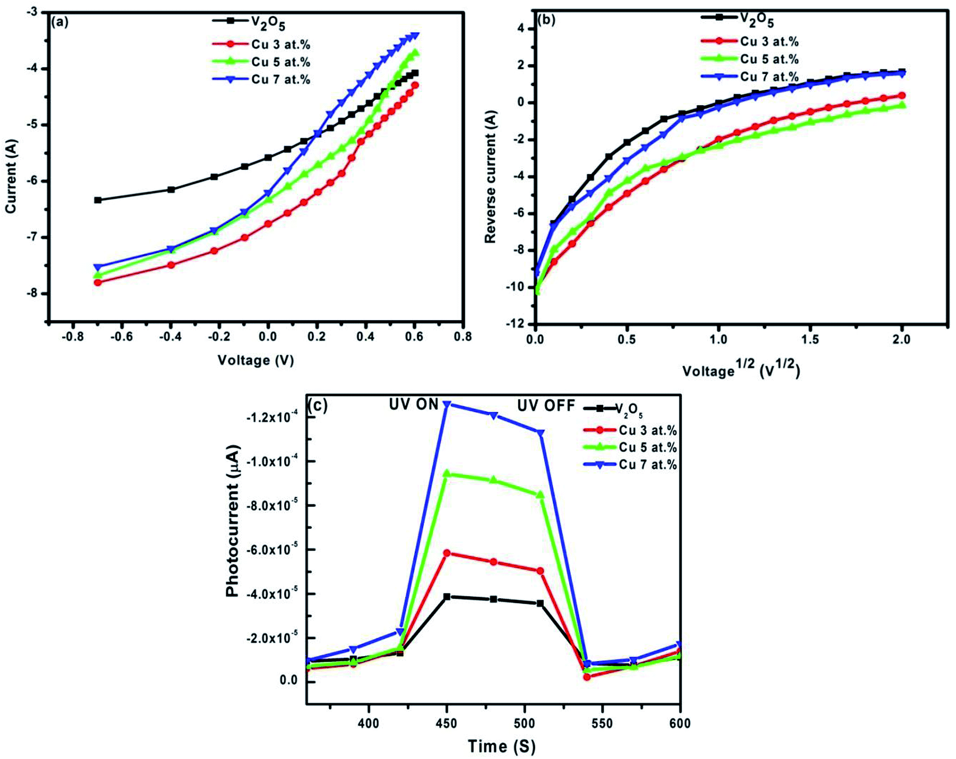
3.7 Current–voltage characteristics of n-CuxV2O5/p-Si diodes
Fig. 8(a–d) show the current–voltage characteristics under dark and illuminated conditions at room temperature of n-V2O5/p-Si and n-CuxV2O5/p-Si diodes. All the I–V characteristics reveal asymmetric and non-ohmic behavior under the dark conditions. The increase in the forward current is due to an increase in photogenerated carriers under illuminated conditions. Hence, the reverse current at a given applied voltage of the diodes under illumination is higher than that of the current in the dark. This possible applied voltage dependence of the reverse current could be attributed to the photo-excitation of the charge carriers from the valence band (Vb) to a defect-perturbed host state. Upon illumination of a diode, electron–hole pairs are generated in the depletion region owing to the absorption of photons with a higher photo-energy than the bandgap of the semiconducting materials. Such rolling progression contributes towards the development of photocurrent alongside the reverse bias direction. Obviously, the pure and doped diodes are found to exhibit good rectifying behavior with illumination. Fig. 8(b–d) represent the forward current response of n-CuxV2O5/p-Si diodes with respect to Cu2+ concentration. The increase in forward current with Cu2+ dopant is due to the rise in carrier concentration, which involves the energy band bending and thus results in a decrease in the width of the depletion region. Fig. 8(e) presents the forward and reverse biased semi-log (J–V) characteristics of the established diodes under dark conditions. As can be seen in the figure, at lower voltages the current of the diodes is reformed exponentially with applied voltage. This confirms the formation of the depletion region in the diodes. These good rectifying properties may be due to the space charge layer formed in the interface of the diodes. The slope of the J–V characteristics in the exponential region depends on two main parameters: i.e., an ideality factor (n) and the reverse saturation current (Is). The ideality factor offers an idea about the recombination process that takes place in the device and the shape of the interfaces. The second parameter, representing the exponential part of the J–V characteristics, is the saturation current, which provides the number of charges capable of rising above the energetic barrier in the reverse bias. According to the thermionic emission current–voltage, the dependence of the junction of the applied voltage may be written as,43| | |
I = Is[exp(qV/nKT) − 1](V ≥ 3KBT/q)
| (10) |
where V is the applied bias voltage, I is the measured current, Is is the saturation current, q is the absolute value of the electronic charge (in C), KB and T are the Boltzmann constant and absolute temperature, respectively, and n is the ideality factor (in the ideal case n = 1; if the transport mechanism is not governed exclusively by a thermionic emission process, n > 1). The saturation current Is is expressed as in eqn (11),| | |
Is = AA*T2exp(−qΦB/KT)
| (11) |
where A* is the Richardson constant, A is the diode area and ΦB is the zero-bias barrier height. The ideality factor, n can be calculated from the straight-line region of the slope during forward bias ln(I)–V plot and can be written as,| | |
n = (q/KT)(dV/d(lnI))
| (12) |
where, Io can be determined by extrapolation of the forward bias ln(I)–V curve to V = 0. ΦB is calculated by the following relation (13),| | |
ΦB = (KT/q)ln(AA*T2/Io)
| (13) |
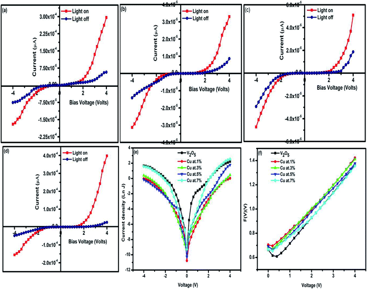 |
| | Fig. 8 I–V characteristics of (a) pure, (c and d) n-CuxV2O5/p-Si, (e) current density–voltage plots of n-CuxV2O5/p-Si p-Si and (f) F(V)–V plot for n-CuxV2O5/p-Si. | |
The values of barrier height (ΦB) and ideality factor (n) are determined from the current-axis intercept and the slope of the linear region of the forward-biased semi-log J–V curve, and the respective values are given Table 2. It can be clearly observed that n-CuxV2O5/p-Si diodes have a lower ideality factor and barrier height values when associated with an n-V2O5/p-Si diode.
Table 2 The optimized electrical parameters of pure and CuxV2O5 samples annealed at 600 °C for 1 h
| CuxV2O5 (x = 0, 3, 5 or 7 at%) |
Barrier height (ΦB) (eV) |
Saturation current (Is) (μA) |
Norde function |
| ΦB (eV) |
Rs (k Ω) |
| 00 |
0.4243 |
3.09 × 10⁻⁵ |
0.4073 |
8.45 × 10² |
| 03 |
0.4373 |
1.88 × 10⁻⁵ |
0.3086 |
1.39 × 10³ |
| 05 |
0.4030 |
6.99 × 10⁻⁵ |
0.2933 |
3.74 × 10² |
| 07 |
0.3837 |
1.46 × 10⁻⁴ |
0.2417 |
1.79 × 10² |
The obtained n value confirms that the resultant currents are due to a recombination and diffusion process in these diodes and the decrease in the ideality factor may be attributed to the improved interface state of the doped diodes.44 Furthermore, the Cu2+ ion substituted V5+ lattice reduces the number of oxygen vacancies, which leads to a lower density of free carriers, which can effectively increase the barrier height at the interface. In addition, Norde introduced another characterization technique to obtain the barrier height (ΦB) and series resistance of device by the following equations:
| | |
F(V) = (Vo/γ) − ((KT/q)I(V))/A*AT2
| (14) |
| | |
ΦB = F(Vo) + (Vo/γ) − (KT/q)
| (15) |
where
I(
V) is current value obtained from the
I–
V curve and
γ is the first integer (dimensionless) greater than the ideality factor of the diode.
F(
Vo) is the minimum point of
F(
V) and
Vo is the corresponding voltage.
Fig. 8(f) shows
F(
V)
vs. V plots for pure and Cu-doped V
2O
5/p-Si diodes, and the respective estimated values are listed in
Table 2.
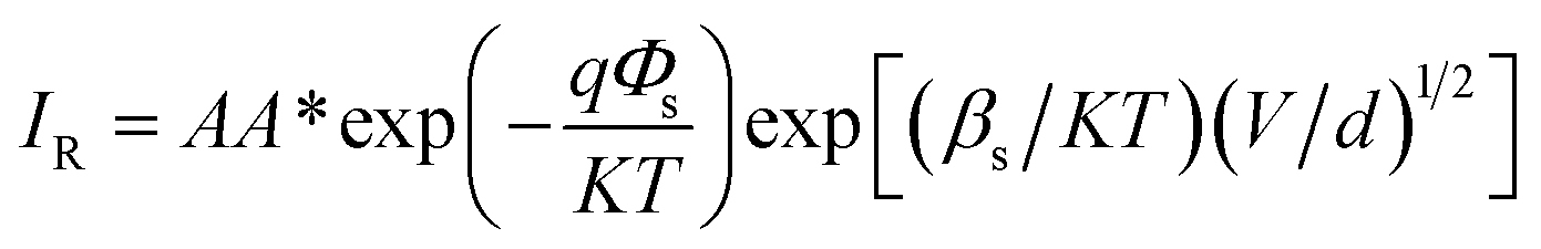
In this regard, the difference between ΦB values obtained from Norde and the I–V method is apparent. This is due to the fact that high series resistance can prevent an accurate evolution of barrier heights from the standard I–V plot. In order to evaluate the conduction mechanism which controls diode behavior, the forward I–V characteristics of the diodes are plotted on a log–log scale and are given in Fig. 9(a). At low voltages, the number of carriers generated thermally is small and the injected carrier density is inadequate, which is referred to as ohmic behavior. When the higher carrier densities from one electrical contact are locally injected into a material, space charge limited current may take place. As seen in the figure, at higher voltages, current is limited when the applied electric field is dominated by the field due to space charge, which is called the space charge limited current (SCLC). The current follows a square dependence on voltage: I ∝ Vm, where m is the slope of the curve. At higher voltages (3 ≤ V ≤ 4), the dominant charge transport mechanism of the diodes is determined by obtaining the slopes of the curves in Fig. 9(a). The exponent m values are found to be 3.25 and 3.10 for n-V2O5/p-Si and n-CuxV2O5/p-Si diodes, respectively. The high values of m (m ≥ 2), indicate an SCLC with an exponential trap distribution.45 To determine the reverse bias charge transport mechanism of the diodes, the various charge transport mechanisms were tested for these diodes. The plots of semi-log JR vs. V1/2 for the n-V2O5/p-Si and n-CuxV2O5/p-Si diodes are shown in Fig. 9(b). As shown in the figure, the reverse currents exhibit two regions and these are interpreted in terms of either the Schottky effect or the Poole–Frenkel effect (field-assisted thermal de-trapping of carriers). For the Schottky mechanism, the current is expressed by the following relation,46
| |
 | (17) |
and the expression for the Poole–Frenkel effect is as follows
| | |
IR = ILFexp[(βPF/KT)(V/d)1/2]
| (18) |
where,
d is the thickness,
βs is the Schottky coefficient,
βPF is the Poole–Frenkel coefficient, and
ILF is the lower field current. The
βs and
βPF coefficients are defined by,
| | |
2βs = βPF = (q3/πεεo)1/2
| (19) |
where
q is carrier charge,
εo is the dielectric constant of a vacuum, and
ε is the dielectric constant of the material (≈6.5).
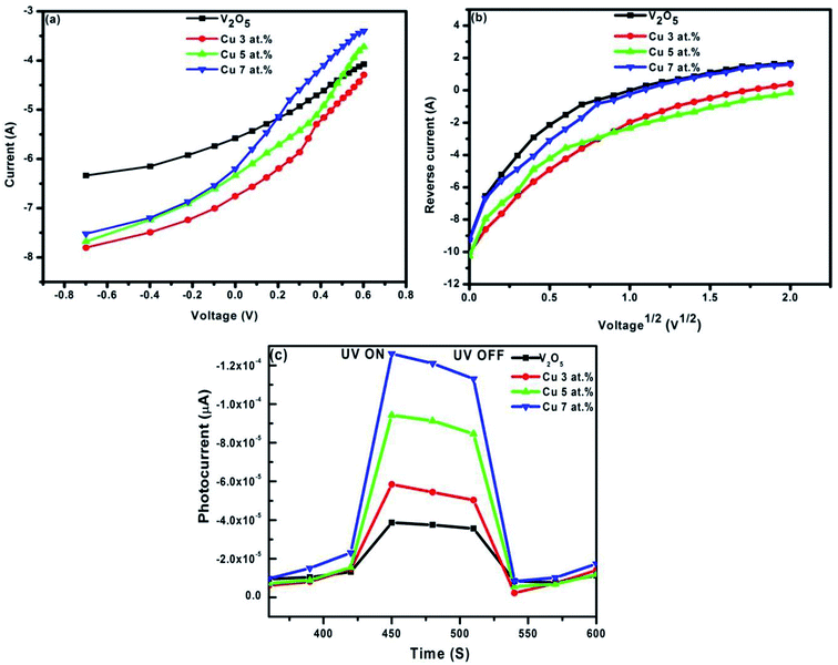 |
| | Fig. 9 Plot of (a) log(I) vs. log(V) characteristics of the pure and CuxV2O5/p-Si diodes and (b) plots of reverse current vs. voltage of pure and CuxV2O5/p-Si diodes and (c) the transient photocurrent of pure and CuxV2O5/p-Si diodes. | |
The theoretical values of βs and βPF were calculated using eqn (13) and were found to be 1.707 × 10⁻¹² and 4.384 × 10⁻¹⁰ eV m1/2 V−1/2, respectively. The obtained values may be attributed to a thermally assisted tunneling field emission of carriers. Furthermore, transient photocurrent time-dependent measurements are a well-known system for analysis of the transport mechanism. Before the experiments, the device was kept in the dark for 15 min to stabilise the current at a constant applied potential. After the stabilization period, the current was captured at each second in the following sequence; 30 seconds in the dark, 30 seconds under illumination. The photoresponse stability of the junction diode was studied by switching the illumination ON and OFF periodically for a number of cycles. The time-resolved photocurrent of the developed diodes is shown in Fig. 9(c). The gradual increase in the photocurrent with respect to illumination indicates trapping of the photogenerated carriers at the band gap states and that decay in the dark current is owing to the thermal de-trapping of the trapped carriers. In addition, the current comes back to its initial state owing to the trapping of the charge carriers in the deep levels under dark conditions. Furthermore, the amount of photocurrent increases with an increase in Cu2+ content compared to the undoped n-V2O5/p-Si diode. As a consequence, it is observed that photodiodes with different Cu2+ concentration indicate photoconduction behavior.
4 Conclusion
We have prepared identical and highly crystalline pure and CuxV2O5 nanorods using a wet chemical precipitation method, using ammonium metavanadate as a source material. The structural analysis showed improved crystallite size and reduced stress and strain values along with phase segregation on varying the Cu doping concentration. SEM analysis depicts homogeneous nanorods for pure V2O5. After doping, the nanorod structure became clustered and changed in shape. The XPS results show the presence of elemental impurities like carbon that originated from the sample; the constituent elements are vanadium, copper and oxygen. The PL intensity was found to be at a maximum for the pure V2O5 sample and luminescence quenching occurred due to Cu substitution. The I–V characteristics and diode performance evaluation show that the electrical properties of the CuxV2O5 nanorods/p-Si diode improved with increasing Cu content as it increased the charge carrier concentration and reduced the defect states in the V2O5 nanorods. Furthermore, our invented n-CuxV2O5/p-Si heterojunction designs are envisaged as potentially respectable candidates for photoresponse applications. This result may provide relief in devaluing the influence of Cu doping on the electrical properties of V2O5 nanorods, which will hopefully be building blocks for a heterojunction optoelectronic device system. In addition, the enhanced diode performance of n-CuxV2O5/p-Si could be attributed to the combined effects of the enhancement in optoelectronics due to the incorporation of an optimal amount of Cu into V2O5.
Conflicts of interest
There are no conflicts to declare.
References
- Y. Zhang, J. Zheng, Q. Wang, T. Hu and C. Meng, RSC Adv., 2016, 6, 93741 RSC.
- R. Wang, S. Yang, R. Deng, W. Chen, Y. Liu, H. Zhang and G. S. Zakharova, RSC Adv., 2015, 5, 41050 RSC.
- S. Rafique, S. M. Abdullah, W. E. Mahmoud, A. A. Al-Ghamdi and K. Sulaiman, RSC Adv., 2016, 6, 50043 RSC.
- X. Liu, J. Zeng, H. Yang, K. Zhou and P. Deng, RSC Adv., 2018, 8, 4014 RSC.
- J. Wu, Y. Zhang, Y. He, C. Liu, W. Guolt and S. Ruan, J. Nanosci. Nanotechnol., 2014, 14, 4214 CrossRef CAS.
- N. Wang, Y. Zhang, T. Hu, Y. Zhao and C. Meng, Curr. Appl. Phys., 2015, 15, 493 CrossRef.
- X. Zhang, M. Wu, S. Gao, Y. Xu, X. Cheng, H. Zhao and L. Huo, Mater. Res. Bull., 2014, 60, 659 CrossRef CAS.
- J. Huang, X. Qiao, Z. Xu, L. Cao, H. Ouyang, J. Li and R. Wang, Electrochim. Acta, 2016, 191, 158 CrossRef CAS.
- S. Zhan, Y. Wei, X. Bie, C. Wang, F. Du, G. Chen and F. Hu, J. Alloy. Comp., 2010, 502, 92 CrossRef CAS.
- R. Abaira, T. Dammak, A. Matoussi and A. Younes, Superlattice. Microst., 2016, 91, 365 CrossRef CAS.
- D. Zhu, H. Liu, L. Lv, Y. D. Yao and W. Z. Yang, Scripta Mater., 2008, 59, 642 CrossRef CAS.
- Q. Song, H. Pang, W. Gong, G. Ning, Y. Zhang, X. Cheng and L. Yuan, Mater. Lett., 2015, 161, 244 CrossRef CAS.
- R. Suresh, K. Giribabu, R. Manigandan, S. Munusamy, S. Praveen Kumar, S. Muthamizh, A. Stephen and V. Narayanan, J. Alloy. Comp., 2014, 598, 151 CrossRef CAS.
- M. Zeng, H. Yin and K. Yu, Chem. Eng. J., 2012, 188, 64 CrossRef CAS.
- V. Petkov, P. N. Trikalitis, E. S. Bozin, S. J. L. Billinge, T. Vogt and M. G. Kanatzidis, J. Am. Chem. Soc., 2002, 124, 10157 CrossRef CAS.
- Y. Weijie, W. Jinxing, G. Zhong ping, Z. Wen, G. Weiwei and L. Liyang, Ceram. Int., 2013, 39, 2639 CrossRef.
- B. Alonso and J. Livage, J. Solid State Chem., 1999, 148, 16 CrossRef CAS.
- C. J. Fontenot, J. W. Wiench, M. Pruski and G. L. Schrader, J. Phys. Chem. B, 2000, 104, 11622 CrossRef CAS.
- T. C. Gujjarahalli, C. Pallellappa, A. Siddaramanan and L. Jacques, Inorg. Chem., 2011, 50, 7421 CrossRef PubMed.
- J. Galy, D. Lavaud, A. Casalot and P. Hagenmuller, J. Solid State Chem., 1970, 2, 531 CrossRef CAS.
- Y. Zhang, J. Zheng, Y. Zhao, T. Hu, Z. Gao and C. Meng, Appl. Surf. Sci., 2016, 377, 385 CrossRef CAS.
- X. L. Zhang, Cryst. Growth Des., 2008, 8, 2609 CrossRef CAS.
- V. Kumar, R. G. Singh, F. Singh and L. P. Purohit, J. Alloy. Comp., 2012, 544, 120 CrossRef CAS.
- N. Senthil kumar, M. Sethu Raman, J. Chandrasekaran, R. Priya, M. Chavali and R. Suresh, Mater. Sci. Semicond. Process., 2016, 41, 497 CrossRef.
- K. Joshi, M. Rawat, S. K. Gautam, R. G. Singh, R. C. Ramola and F. Singh, J. Alloys Compd., 2016, 680, 252 CrossRef CAS.
- M. Chen, Z. L. Pei, C. Sun, L. S. Wen and X. Wang, J. Cryst. Growth, 2000, 220, 254 CrossRef CAS.
- R. Ghosh, D. Basak and S. Fujihara, J. Appl. Phys., 2004, 96, 2689 CrossRef CAS.
- H. Schulz and K. H. Thiemann, Solid State Commun., 1979, 32, 783 CrossRef CAS.
- M. Hafeez, U. Manzoor, A. S. Bhatti, B. Karnayar and S. I. Shah, J. Appl. Phys., 2012, 111, 024313 CrossRef.
- H. J. Fan, B. Fuhrmann, R. Scholz, C. Himcinschi, A. Berger, H. Leipner, A. Dadgar, A. Krost, S. H. Christiansen, U. Gosele and M. Zacharias, Nanotechnology, 2006, 17, 231 CrossRef.
- C. W. Zou, Y. F. Rao, A. Alyamani, W. Chu, M. J. Chen, D. A. Patterson, E. A. C. Emanuelsson and W. Gao, Langmuir, 2010, 26, 11615 CrossRef CAS PubMed.
- Y. S. Hu, X. Liu, J. O. Muller, R. Schlogl, J. Maier and D. S. Su, Angew. Chem., Int. Ed., 2009, 48, 210 CrossRef CAS PubMed.
- D. Chakraborti, G. R. Trhchy, J. T. Prater and J. Narayan, J. Phys. D: Appl. Phys., 2007, 40, 7606 CrossRef CAS.
- G. Schon, Surf. Sci., 1973, 35, 96 CrossRef CAS.
- I. Nakai, Y. Sugitani, K. Nagashima and Y. Niwa, J. Inorg. Nucl. Chem., 1978, 40, 789 CrossRef CAS.
- K. Karthika and K. Ravichandran, J. Mater. Sci. Technol., 2015, 31, 1111 CrossRef.
- B. X. Lin, Z. X. Fu and Y. B. Jia, Appl. Phys. Lett., 2001, 79, 943 CrossRef CAS.
- K. Dutta and R. J. Nelson, J. Appl. Phys., 1982, 53, 74 CrossRef.
- X. B. Wang, C. Song, K. W. Geng, F. Zeng and F. Pan, Appl. Surf. Sci., 2007, 253, 6905 CrossRef CAS.
- M. Anpo, S. G. Zhang, S. Higashimoto, M. Matsuoka and H. Yamashita, J. Phys. Chem. B, 1999, 103, 9295 CrossRef CAS.
- N. V. Hullavarad, S. S. Hullavarad and P. C. Karulkar, J. Electrochem. Soc., 2008, 155, K84 CrossRef CAS.
- E. H. Rhoderick and R. H. Williams, Metal-Semiconductor Contacts, Clarendon, Oxford, 2nd edn, 1988, p. 252 Search PubMed.
- P. Klason, M. M. Rahman, Q.-H. Hu, O. Nur, R. Turan and M. Willander, Microelectron. J., 2009, 40, 706 CrossRef CAS.
- H. M. Zhang and W. C. H. Choy, IEEE Trans. Electron Devices, 2008, 55, 2517 CAS.
- Ş. Aydoğan, K. Çınar, H. Asıl, C. Coşkun and A. Türüt, J. Alloys Compd., 2009, 476, 913 CrossRef.
- J. H. Evans-Freeman, M. M. El-Nahass, A. A. M. Farag and A. Elhaji, Microelectron. Eng., 2011, 88, 3353 CrossRef CAS.
Footnote |
| † Electronic supplementary information (ESI) available: TG/DTA studies (Fig. S1 and S2). See DOI: 10.1039/c8ra07717g |
|
| This journal is © The Royal Society of Chemistry 2019 |
Click here to see how this site uses Cookies. View our privacy policy here. 
 Open Access Article
 This Open Access Article is licensed under a Creative Commons Attribution-Non Commercial 3.0 Unported Licence
 *a and
T. Elangovan
*a and
T. Elangovan