
 Open Access Article
 This Open Access Article is licensed under a Creative Commons Attribution-Non Commercial 3.0 Unported Licence
Replacement of n-type layers with a non-toxic APTES interfacial layer to improve the performance of amorphous Si thin-film solar cells†
Hassan Hafeez‡
 a,
Dae Keun Choi‡a,
Chang Min Lee‡a,
P. Justin Jesuraja,
Dong Hyun Kima,
Aeran Songb,
Kwun Bum Chungb,
Myungkwan Songc,
Jun Fei Mac,
Chang-Su Kim*c and
Seung Yoon Ryu*a
a,
Dae Keun Choi‡a,
Chang Min Lee‡a,
P. Justin Jesuraja,
Dong Hyun Kima,
Aeran Songb,
Kwun Bum Chungb,
Myungkwan Songc,
Jun Fei Mac,
Chang-Su Kim*c and
Seung Yoon Ryu*a
aDivision of Display and Semiconductor Physics, Display Convergence, College of Science and Technology, Korea University Sejong Campus, 2511 Sejong-ro, Sejong City, 30019, Republic of Korea. E-mail: justie74@korea.ac.kr; cskim1025@kims.re.kr
bDivision of Physics and Semiconductor Science, Dongguk University, Seoul 04620, Republic of Korea
cAdvanced Nano-Surface Department, Korea Institute of Materials Science (KIMS), Changwon, 51508, Republic of Korea
First published on 6th March 2019
Abstract
Hydrogenated amorphous Si (a-Si:H) thin-film solar cells (TFSCs) generally contain p/n-type Si layers, which are fabricated using toxic gases. The substitution of these p/n-type layers with non-toxic materials while improving the device performance is a major challenge in the field of TFSCs. Herein, we report the fabrication of a-Si:H TFSCs with the n-type Si layer replaced with a self-assembled monolayer (3-aminopropyl) triethoxysilane (APTES). The X-ray photoelectron spectroscopy results showed that the amine groups from APTES attached with the hydroxyl groups (–OH) on the intrinsic Si (i-Si) surface to form a positive interfacial dipole towards i-Si. This interfacial dipole facilitated the decrease in electron extraction barrier by lowering the work function of the cathode. Consequently, the TFSC with APTES showed a higher fill factor (0.61) and power conversion efficiency (7.68%) than the reference device (without APTES). This performance enhancement of the TFSC with APTES can be attributed to its superior built-in potential and the reduction in the Schottky barrier of the cathode. In addition, the TFSCs with APTES showed lower leakage currents under dark conditions, and hence better charge separation and stability than the reference device. This indicates that APTES is a potential alternative to n-type Si layers, and hence can be used for the fabrication of non-toxic air-stable a-Si:H TFSCs with enhanced performance.
Introduction
The photovoltaic technology, which converts solar energy into electricity has been extensively studied,1,2 leading to the development of hydrogenated amorphous Si (a-Si:H) thin film solar cells (TFSCs).3,4 They are favorable due to their simple and inexpensive fabrication, possibility of deposition on flexible/bendable substrates5,6 and the highly transparent nature has been recently exploited for “building integrated photovoltaic (BIPV)” systems.7,8 However, the greatest challenge in further development of high performance a-Si:H TFSCs is without (w/o) the involvement of hazardous/toxic doping gases.5,6,9,10 The fabrication of such devices should be carried out under extremely safe environments. In addition, the use of hazardous/toxic doping gases causes device instabilities because of carrier trapping and the formation of Si dangling bonds.5,6 Many alternate processes have been investigated and toxic-free layers have been utilized using various processes in the fabrication of a-Si:H TFSCs. For example, Jung et al.9 demonstrated the deposition of a V2O5−x window layer using RF magnetron sputtering as an efficient replacement of p-type silicon layer resulting in a power conversion efficiency (PCE) of about 7.04%. Ryu et al.5 presented the scheme for replacement of both p- and n-type layers with MoO3 and LiF, respectively processed with thermal deposition achieving a PCE of ∼7.08%. Furthermore, in crystalline silicon solar cells, Battaglia et al.11 substituted the p-type Si layer with MoO3 and achieved a PCE of 14% while, Bullock et al.12 presented a maximum efficiency of 20% by incorporating dopant-free alkali metal fluorides and metal oxides for electron and hole selective carriers, respectively. Masuda et al.13 exhibited a completely toxic-free and solution-processable method for the deposition of p-type, n-type and amorphous (intrinsic) i-Si layers. However, the low PCE (0.3–0.51%) makes it unsuitable for the commercial adoption and therefore, the exploration of other alternatives is highly desirable.Among all the alternatives, materials with amine groups (–NH2) have drawn greater attention as they are not only dopant-free but are also capable of generating an interfacial dipole, which can effectively tune the work function (φ) of the electrodes.6,14 In this regard, Song et al.15 proposed a promising approach to fabricate air-stable inverted organic solar cells using a self-assembled monolayer (SAM) of 3-aminopropyltriethoxysilane (APTES). However, it is to be noted that in majority of the proposed methods, the orientation of the APTES molecule initiated with –Si binding itself on the substrate and –NH2 facing outwards close to the cathode.15,16 This resulted in the generation of a positive interfacial dipole17 from the cathode towards the active layer. Interestingly, in this study, the orientation of APTES was in the opposite direction, i.e. the –NH2 groups bonded with the hydroxyl (–OH) groups present on the substrate through hydrogen bonding, as revealed by the X-ray photoelectron spectroscopy (XPS) and as demonstrated by Acres et al.18 In this study, we investigated the performance of the SAM interfacial layer (APTES) with inverse orientation as an alternative to n-type layers for a-Si:H TFSCs. To the best of our knowledge such an investigation has not been carried out till date. The APTES SAM generated an interfacial dipole, lowering the φ of the cathode. This lowering of φ improved the charge extraction from the active layer. The devices with an APTES n-type interfacial layer showed significantly higher fill factors (FFs), PCEs, and stability (low leakage current) than the TFSCs w/o APTES.
Experimental
Materials and methods
Textured fluorine-doped tin oxide (FTO, Pilkington)-coated glass (Type NSG TEC™ 7 with a sheet resistance of 6–8 Ω sq−1, thickness of about 3 mm, visible light transmittance 80–82%) was cleaned by ultrasonication and rinsing in ethanol and deionized water (DI) for 15 min. The intrinsic Si (i-Si) layer (500 nm) was deposited using a mixture of silane (SiH4) and hydrogen (H2) (50 sccm/50 sccm) with chamber's working pressure of 400 mTorr with a very high frequency (VHF, 40.7 MHz) and power of 20 W. The p-type Si layer (12 nm) was deposited under the RF power of 50 W using a combination of different gases including SiH4/H2 (30 sccm/150 sccm) and B2H6 (9 sccm). For both layers, the plasma-enhanced chemical vapor deposition (PECVD) power density was maintained at 0.074 W cm−2 keeping the electrode dimensions in consideration. Approximately 15.7 mm distance was maintained between the shower head and the upper electrode at 250 °C.In order to develop a silanol-terminated i-Si layer, we used ultra-violet ozone at 187 nm for 20 min, which increased the amount of O and H components on the surface. The APTES solution was purchased (≥98% purity, Sigma Aldrich, USA) with a shelf-life of 2 years and was used w/o any further processing. A thin APTES layer (∼2 nm) was spin coated on the i-Si layer at 2000 rpm for 40 s followed by drying18 for 60 s. The APTES layer is usually unstable under intense environmental conditions such as presence of moisture, high humidity and any other chemical substances,19 therefore, to eliminate any possible adverse effects, the deposition process was conducted in a glove box with a precise control of humidity/temperature. After deposition of APTES layer, the substrate was immediately transferred to the vacuum chamber where a double layer of LiF (1.5 nm)/Al (100 nm) was deposited as the cathode at a base pressure of ∼2 × 10⁻⁶ torr. A shadowed mask was used by thermal evaporation to define the active area (0.25 cm2) of the cell. The overall process ensured that the APTES layer was not considerably exposed to any harsh environmental/chemical conditions and indicates its adequate stability.
Characterizations
The surface morphology of the deposited APTES layer was examined using a multimode 8 atomic force microscope (AFM, Bruker) equipped with a Nanoscope V controller. The AFM measurements were carried out in the tapping mode at room temperature with 384 × 384 pixels over a scan size of 3 × 3 μm at a scan rate of 1 Hz. We used an Al-coated silicon probe (NCHR, Nanoworld, Germany) with a nominal spring constant of 40 N m−1 and a resonance frequency of 320 kHz. The compositional analysis was carried out using X-ray photoelectron spectroscopy (XPS, VG Microtech ESCA 2000). An Al Kα photon source was used to examine the composition of the APTES layer. The chemical bonding states of the layers were investigated in detail using their N1s and Si2p spectra normalized and de-convoluted with difference Gaussian peaks. Ultraviolet photoelectron spectroscopy (UPS) analysis was carried out at an energy resolution of 0.05 eV and the samples were biased at −15.0 V. The performance of the a-Si:H TFSCs under light and dark conditions was evaluated using a Keithley 2400 source meter with an intensity of 100 mW cm−2. The simulated illumination using a solar simulator (Peccell Technologies, PEC-L11) was carried out under AM1.5. The external quantum efficiency of the devices was measured using an incident photocurrent efficiency measurement system equipped with a 200 W Xe lamp and a grating monochromator. The light intensity measurements were carried out using a calibrated Si solar cell. The device efficiency data in Table 1 presents the average performance from 5 devices with a cell active area of 0.25 cm2 and the approximate yield of the devices was observed to be more than 60%. The surface wettability of the APTES layer was analyzed using the smart drop standard (FEMTOBIOMED, South Korea). The contact angle (CA) system was integrated with single non-approximated algorithm numerical calculations of Bash forth-admans (equation) and was free from disturbance. An ultra high-resolution field emission scanning electron microscope (UHR FE-SEM, S-5500, Hitachi, at Korea Basic Science Institute, Jeonju Center) was used at an accelerating voltage of 7 kV for the analysis of the surface morphology of the layers.| Device structure | Jsc (mA cm−2) | Voc (V) | FF (fill factor) | PCE (%) | Rs (Ω cm2) | RSH (Ω cm2) |
|---|---|---|---|---|---|---|
| a The data has been reported before, using the same fabrication tool and conditions as mentioned in this work and was added in the table for comparison purpose. | ||||||
| FTO/P–I Si/Al | 13.82 ± 0.12 | 0.63 ± 0.01 | 0.48 ± 0.01 | 4.30 ± 0.06 | 18.20 | 3.2 × 10³ |
| FTO/P–I Si/APTES/Al | 14.42 ± 0.10 | 0.75 ± 0.01 | 0.50 ± 0.01 | 5.52 ± 0.05 | 27.60 | 7.35 × 10³ |
| FTO/P–I Si/LiF/Al | 15.62 ± 0.15 | 0.78 ± 0.01 | 0.58 ± 0.01 | 7.18 ± 0.06 | 12.00 | 9.92 × 10³ |
| FTO/PIN-Si/Ala,10 | 15.15 | 0.82 | 0.61 | 7.60 | 6.4 | 6.1 × 10³ |
| FTO/PI-Si/PFN/Ala,6 | 15.04 | 0.80 | 0.59 | 7.17 | 19.0 | 1.1 × 10⁵ |
| FTO/P–I Si/APTES/LiF/Al | 15.51 ± 0.08 | 0.80 ± 0.01 | 0.61 ± 0.01 | 7.68 ± 0.03 | 11.70 | 9.52 × 10³ |
Results and discussion
Fig. 1(a) the schematic of the a-Si:H TFSCs device structure using the conventional layout (textured fluorine-doped tin oxide (FTO, Pilkington)/p-type Si/intrinsic Si (i-Si)/APTES/lithium fluoride (LiF)/Al). Due to the requirement of toxic/hazardous doping gases in the processing of n-type layer deposition, APTES was utilized as the replacement. This SAM layer consists of a specific molecular arrangement owing to the presence of –NH2, silane, and carboxyl groups (–C![[double bond, length as m-dash]](https://www.rsc.org/images/entities/char_e001.gif) O).15,20,21 The positive and negative charge distributions on –NH2 and –O, respectively created a dipole moment, which depended on the electron withdrawing and donating natures of the atoms placed transversely in the molecule (Fig. 1(b)).16 It is well-known that in APTES-related processes, the silane present in APTES attached itself to the substrate through hydrogen bonding, while the –NH2 groups pointing outwards contribute to the generation of an interfacial dipole with a dipole direction opposite to the direction of electron extraction.15,16 However, in this study, the molecular orientation of the APTES deposited on i-Si was reversed (Fig. 1(b)), where –NH2 attached to the –OH from i-Si through hydrogen bonding while silane and –CO (EtO) acted as the terminal groups near the LiF/Al cathode. Consequently, an interfacial dipole with the dipole direction opposite to the direction of electron extraction was obtained thus reducing the electron extraction barrier (δ). The presence of these functional groups and orientation was analyzed in detail using XPS (Fig. 2) with full survey shown in Fig. S1.† Fig. 2(a) shows the Si2p XPS spectra of the bare and APTES-treated i-Si layers. The APTES-treated i-Si layer showed Si–O bonds (100% contribution) at ∼103 eV.22 The bare i-Si sample showed an additional Si–O peak with ∼22% contribution at ∼102 eV (Fig. 2(d)) along with the bulk Si peak at ∼99 eV.23 This could be attributed to the oxidation/hydroxylation of bare i-Si, leading to the availability of –OH groups on the layer surface. The N1s profile15 of the APTES-treated i-Si layer showed the presence of free –NH2 groups (∼400 eV) from APTES (Fig. 2(a)). The deconvolution process (Fig. 2(c)) revealed the presence of an additional –NH2 peak at ∼401 eV (with 20% contribution) corresponding to the hydrogen-bonded –NH2 (NH3).18 This analysis provided a concrete evidence for the inverse molecular orientation of APTES on i-Si, as mentioned above and reported previously.18 Regarding the nature of the APTES bonding with the i-Si surface, Kim et al.24 reported that the APTES films could be formed in both covalent and non-covalent (physical bond) manners, however if the process is carried out using aqueous solutions, the greater probability favors the formation of hydrogen bonds or electrostatic interactions (van der Waals). In our work, the APTES layers were deposited using spin coating of the APTES solution onto the i-Si substrate, therefore we could speculate the establishment of hydrogen bonds between APTES (–NH2) and –OH from the i-Si substrate. The deposition process for device fabrication was carried out in a glove box, however for UPS/XPS analysis, the samples were taken out of the chamber and transferred. As APTES is a hydrolytically unstable material,25 an exposure to air/moisture might have disengaged the weak hydrogen bonds or even possibly reoriented the molecules due to the change in molecular environment.18 Therefore, the observed contribution (20%) only provides an indication about the possible orientation of the molecules on the surface. However, if we may perform XPS/UPS analysis within the controlled environmental conditions (in situ measurement), it might be possible to observe an appropriate percentage of the NH2–H bonding. Overall, this orientation of APTES on i-Si was found to be coherent with the attachment possibilities of APTES on Si substrates demonstrated by Acres et al.18 (Fig. S2†) and is also in accordance with the decrease in work function observed due to the interfacial dipole (towards i-Si). The surface morphologies of the bare and APTES-treated i-Si layers were examined using atomic force microscopy (AFM, Fig. S3†) and were further analyzed by the ultra-high-resolution field emission scanning electron microscopy (UHR FE-SEM, Fig. S4†). Because of the underlying FTO with a surface roughness of 30.81 ± 0.3 nm,26 the bare i-Si layer samples demonstrated a matching surface roughness (root mean square (RMS) = ∼30.21 ± 0.1 nm) and hence a higher contact angle (CA = ∼63°) of water droplet with the surface was observed (Fig. S4†). The RMS value for the APTES-based i-Si layer (29.69 ± 0.1 nm) was also found to be almost similar indicating a uniform deposition of the layer. However, a significant decrease in the CA (to ∼29°) of the APTES-treated i-Si layer was because of the presence of an interfacial dipole (chemical aspect, Fig. S4†) generated by the APTES layer.
O).15,20,21 The positive and negative charge distributions on –NH2 and –O, respectively created a dipole moment, which depended on the electron withdrawing and donating natures of the atoms placed transversely in the molecule (Fig. 1(b)).16 It is well-known that in APTES-related processes, the silane present in APTES attached itself to the substrate through hydrogen bonding, while the –NH2 groups pointing outwards contribute to the generation of an interfacial dipole with a dipole direction opposite to the direction of electron extraction.15,16 However, in this study, the molecular orientation of the APTES deposited on i-Si was reversed (Fig. 1(b)), where –NH2 attached to the –OH from i-Si through hydrogen bonding while silane and –CO (EtO) acted as the terminal groups near the LiF/Al cathode. Consequently, an interfacial dipole with the dipole direction opposite to the direction of electron extraction was obtained thus reducing the electron extraction barrier (δ). The presence of these functional groups and orientation was analyzed in detail using XPS (Fig. 2) with full survey shown in Fig. S1.† Fig. 2(a) shows the Si2p XPS spectra of the bare and APTES-treated i-Si layers. The APTES-treated i-Si layer showed Si–O bonds (100% contribution) at ∼103 eV.22 The bare i-Si sample showed an additional Si–O peak with ∼22% contribution at ∼102 eV (Fig. 2(d)) along with the bulk Si peak at ∼99 eV.23 This could be attributed to the oxidation/hydroxylation of bare i-Si, leading to the availability of –OH groups on the layer surface. The N1s profile15 of the APTES-treated i-Si layer showed the presence of free –NH2 groups (∼400 eV) from APTES (Fig. 2(a)). The deconvolution process (Fig. 2(c)) revealed the presence of an additional –NH2 peak at ∼401 eV (with 20% contribution) corresponding to the hydrogen-bonded –NH2 (NH3).18 This analysis provided a concrete evidence for the inverse molecular orientation of APTES on i-Si, as mentioned above and reported previously.18 Regarding the nature of the APTES bonding with the i-Si surface, Kim et al.24 reported that the APTES films could be formed in both covalent and non-covalent (physical bond) manners, however if the process is carried out using aqueous solutions, the greater probability favors the formation of hydrogen bonds or electrostatic interactions (van der Waals). In our work, the APTES layers were deposited using spin coating of the APTES solution onto the i-Si substrate, therefore we could speculate the establishment of hydrogen bonds between APTES (–NH2) and –OH from the i-Si substrate. The deposition process for device fabrication was carried out in a glove box, however for UPS/XPS analysis, the samples were taken out of the chamber and transferred. As APTES is a hydrolytically unstable material,25 an exposure to air/moisture might have disengaged the weak hydrogen bonds or even possibly reoriented the molecules due to the change in molecular environment.18 Therefore, the observed contribution (20%) only provides an indication about the possible orientation of the molecules on the surface. However, if we may perform XPS/UPS analysis within the controlled environmental conditions (in situ measurement), it might be possible to observe an appropriate percentage of the NH2–H bonding. Overall, this orientation of APTES on i-Si was found to be coherent with the attachment possibilities of APTES on Si substrates demonstrated by Acres et al.18 (Fig. S2†) and is also in accordance with the decrease in work function observed due to the interfacial dipole (towards i-Si). The surface morphologies of the bare and APTES-treated i-Si layers were examined using atomic force microscopy (AFM, Fig. S3†) and were further analyzed by the ultra-high-resolution field emission scanning electron microscopy (UHR FE-SEM, Fig. S4†). Because of the underlying FTO with a surface roughness of 30.81 ± 0.3 nm,26 the bare i-Si layer samples demonstrated a matching surface roughness (root mean square (RMS) = ∼30.21 ± 0.1 nm) and hence a higher contact angle (CA = ∼63°) of water droplet with the surface was observed (Fig. S4†). The RMS value for the APTES-based i-Si layer (29.69 ± 0.1 nm) was also found to be almost similar indicating a uniform deposition of the layer. However, a significant decrease in the CA (to ∼29°) of the APTES-treated i-Si layer was because of the presence of an interfacial dipole (chemical aspect, Fig. S4†) generated by the APTES layer.
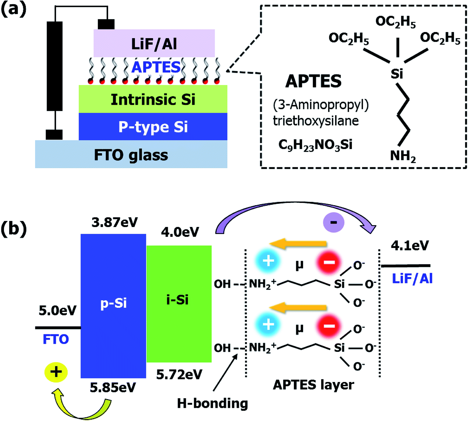 | ||
| Fig. 1 (a) Schematic of the a-Si:H TFSCs with APTES as the n-type layer. Chemical structure of APTES demonstrating the presence of –NH2, –Si, and –CO functional groups with an inverse orientation and dipole direction towards the i-Si layer. (b) Band-gap alignment of the layers used in the devices with APTES as an interfacial layer between the i-Si layer and the cathode demonstrating the arrangement of APTES molecules on the i-Si layer and the direction (yellow arrow) of the interfacial dipole. | ||
 | ||
| Fig. 2 High resolution (a) Si2p and (b) N1s XPS profiles of the bare i-Si and APTES-treated i-Si layers to analyze the composition of the layer and nature of bonds. (c) Si2p and (d) N1s spectra were carefully normalized and de-convoluted with difference Gaussian peaks and the table summarizes the contribution of the analyzed functional groups and bonds. | ||
Fig. 3(a and b) shows the changes in the Fermi level (Fermi edge) of the i-Si layer after the deposition of the APTES layer. The i-Si layer had a φ of ∼1.72 eV, and the deposition of APTES resulted in the generation of interface dipoles in the i-Si/cathode interface, which in turn reduced the electron interface barrier significantly. This improved the vacuum level between the i-Si layer and the cathode, which caused a reduction of ∼0.5 eV in the electron barrier. Even though, the φ changes were observed for the i-Si layer and not for the LiF/Al cathode, and the reduction was oddly high (1.2 eV) (Fig. 3(c and d)), which could be due to the un-wanted oxidation of the i-Si layer owing to delayed ultraviolet photoelectron spectroscopy (UPS) measurement. However, APTES deposition reduced the φ of the cathode by ∼0.5 eV.15 The analysis suggests that the deposition of APTES resulted in the reduction of the Schottky barrier at the interface between the i-Si layer and the cathode. This improved the built-in potential (Vbi) and band-gap alignment for efficient electron extraction, while suppressing the charge recombination.6 This enhancement could be observed from the current density–voltage (J–V) characteristics of the a-Si:H TFSCs analyzed under light (Fig. 4(a)) and dark conditions (Fig. 4(b)). The device performance parameters such as the short-circuit current (Jsc), open-circuit voltage (Voc), FF, and PCE are summarized in Table 1. The FTO/PIN-Si/Al10 device performance incorporated for comparison in the table were realized using the same fabrication tool and conditions as mentioned in this work and therefore can be suitably utilized for evaluation purposes. The comparison of devices w/o and with APTES using Al cathode demonstrated the worst Jsc (13.82 mA cm−2) and Voc (0.63 V), which was improved to 14.42 mA cm−2 and 0.75 V, respectively with the insertion of APTES. In general, the overall lower Voc observed for all devices could be further enhanced by proper optimization of the process conditions for deposition of i-Si.
 | ||
| Fig. 3 (a) Normalized UPS spectra showing the Fermi levels of the bare i-Si and APTES-treated i-Si layers (b) enlarged (smaller scale) spectra to demonstrate the difference between the Fermi edges (c) δ at the interface w/o APTES, (d) reduced δ upon the addition of APTES layer. | ||
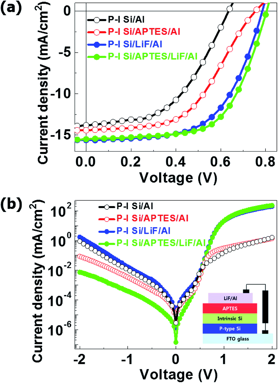 | ||
| Fig. 4 Current density–voltage (J–V) curves of the devices w/o and with APTES layer, also the comparison with the presence/absence of LiF at the cathode (a) under illumination (b) under dark conditions. | ||
Also, the shunt resistances (RSH) of the devices with and w/o APTES were found to be 7.35 × 10³ and 3.2 × 10³ Ω cm2, respectively. This indicates that APTES reduced the φ of the cathode, and hence enhanced the electron extraction and Vbi by the generation of an interfacial dipole. However, a discrepancy in terms of series resistance (Rs) was observed, where despite of providing a higher Voc, the APTES-treated devices demonstrated a high Rs of ∼27.60 Ω cm2 as compared to the device w/o APTES (18.20 Ω cm2) (Table 1). This can be attributed to the reverse polarization of the APTES molecules near the surface of the Al cathode, which occurred because of the direct contact of the SAM layer with the metal surface (Fig. S5†).17 The polarization of APTES molecules reversed the dipole direction at the APTES/Al cathode interface, thus reducing the net dipole. The direct contact of APTES with Al increased the Rs and would have decreased the Jsc however, the Jsc was improved. The Jsc of TFSCs depends on their Rs and Voc. In this study, the addition of the n-type APTES layer improved the Voc of the TFSCs significantly, which in turn improved the Jsc.10,17 The polarization effect was not observed when a LiF layer was used at the Al cathode. This prevented the direct contact between APTES and the metal surface. However, it is possible to overall improve the Rs of a device by utilizing different techniques to enhance the front/rear electrode contact with the underlying silicon layers. Moreover, the presence of a LiF layer in TFSCs reduces the φ of the cathodes.27 Hence, the LiF/Al cathode devices w/o APTES showed higher Jsc (15.62 mA cm−2) and Voc (0.78 V) than the Al cathode devices. The incorporation of APTES in the LiF/Al cathode TFSCs, further enhanced their Voc to 0.80 V and reduced the Jsc slightly to 15.51 mA cm−2. This discrepancy could be due to two reasons: first that the interfacial dipole was not efficiently generated by APTES, which was not the case as observed by the improvement of Jsc and Voc in Al cathode device. Also, the creation of an interfacial dipole mainly improves the Vbi as mentioned before28,29 and the resulting Voc for APTES incorporated devices was enhanced. Second, the addition of LiF increased the thickness of the interface between the i-Si layer and the Al cathode, thus increasing the Schottky barrier slightly. This is consistent with the slightly lowered Jsc and increased Voc of the APTES-treated devices. The low Rs (Table 1) of the APTES-based devices (11.70 Ω cm2) as compared to that of the reference device (12 Ω cm2) confirms that the addition of APTES improved the Vbi of the device by generating an interfacial dipole. The devices with (9.52 × 10³ Ω cm2) and w/o (9.92 × 10³ Ω cm2) APTES showed similar RSH values, indicating the saturation of RSH. Moreover, the J–V analysis under dark conditions of the devices w/o APTES (with LiF only) showed high leakage currents and hence low stability. This could be attributed to the low thickness and density of the LiF layer w/o APTES, which might have resulted in a poor thin-film coverage.5,9 The addition of APTES with LiF reduced the leakage current and improved the Voc of the devices significantly, which indicates that the addition of APTES improved the LiF layer density by providing adequate thin-film coverage and suppressed the charge recombination. Moreover, in terms of device stability enhancement Wang et al.30 presented that the deposition of a thin (∼5 nm) APTES SAM could efficiently inhibit the diffusion of metals into adjacent dielectrics and could simultaneously improve the interfacial adhesion. Also, Ohta K. et al.31 demonstrated a combination layer of CoWB and APTES to suppress Cu diffusion into SiO2. Therefore, we could speculate that the use of APTES/LiF combination in our fabricated a-Si:H TFSC devices could significantly suppress the Al (cathode metal) diffusion into the amorphous silicon layers, thus improving the stability of the devices. We also evaluated the device performance of APTES a-Si:H TFSCS with the reported values of conventional P–I–N device10 and another amine-based conjugated polymer interlayer poly[(9,9-bis(3′-(N,N-dimethylamino)propyl)-2,7-fluorene)-alt-2,7(9,9-dioctylfluorene)] (PFN)-based solar cell.6 In comparison to P–I–N devices, APTES TFSCs demonstrated an enhanced Jsc, PCE and RSH even though FF remained unchanged due to an increased Rs attributed to the different nature of the interfacial contacts. While, in comparison to the PFN devices (amine-based), APTES-treated TFSCs exhibited superior performance in all device parameters. Overall, the APTES-incorporated devices exhibited higher FF (0.61) and PCE (7.68%) attributed to their enhanced Vbi, electron extraction and stability, thus projecting this toxic-free SAM layer as a competent alternative to other n-type/conjugated polymer layers in a-Si:H TFSCs.
Conclusions
In this study, we used APTES as an alternative to n-type layers for a-Si:H TFSCs with improved performance and stability. The facile solution processability of the APTES layer w/o the involvement of any toxic doping gases is highly advantageous for the development of hazard-free solar cells. The –NH2 groups from the deposited APTES layer reacted with the –OH groups on the i-Si surface through hydrogen bonding to form a positive interfacial dipole towards the i-Si layer (opposite to the direction of electron extraction). The interfacial dipole generated by the APTES layer decreased the Schottky barrier at the interface and φ of the cathode. This resulted in enhanced electron extraction, suppressed charge recombination, and improved Vbi. As a result, the devices with APTES showed enhanced Voc (0.80), FF (0.61), and PCE (7.68%) as compared to the devices w/o APTES. The low leakage current of the APTES-based TFSCs presented a strong stability of the devices, which further acknowledges the improvement in device performance and significance of the proposed method.Author contributions
S. Y. R. and C. S. K. are corresponding authors designed and conceived this work. H. H. and P. J. J. drafted the manuscript by providing comprehensive analysis. D. H. K., and D. K. C. fabricated the solar cell devices. C. M. L. and J. F. M. participated in the electrical characterizations. A. S. and K. B. C. analyzed the XPS/UPS results in details. M. K. S. provided valuable analysis and discussion.Conflicts of interest
The authors declare no conflicts of interests.Acknowledgements
This research was supported by Basic Science Research Program through the National Research Foundation of Korea (NRF) funded by the Ministry of Education (NRF-2014R1A6A1030732 and 2017R1A2B4005583). This work was also supported by “Human Resources Program in Energy Technology” of the Korea Institute of Energy Technology Evaluation and Planning (KETEP), granted financial resource from the Ministry of Trade, Industry & Energy, Republic of Korea (No. 20184030201910). This research was also supported by the “Nano Product Upgrading Program using Electron Beam” through the Gyeongsangnam-do & Gimhae.Notes and references
- A. Polman, M. Knight, E. C. Garnett, B. Ehrler and W. C. Sinke, Science, 2016, 352, aad4424 CrossRef PubMed.
- H. Kang, G. Kim, J. Kim, S. Kwon, H. Kim and K. Lee, Adv. Mater., 2016, 28, 7821–7861 CrossRef CAS PubMed.
- S. De Wolf, A. Descoeudres, Z. C. Holman and C. Ballif, Green, 2012, 2, 7–24 CAS.
- A. G. Aberle, Thin Solid Films, 2009, 517, 4706–4710 CrossRef CAS.
- J.-H. Yang, H.-H. Jung, J. Seo, K.-D. Kim, D.-H. Kim, D.-C. Lim, S.-G. Park, J.-W. Kang, M. Song, M.-S. Choi, J.-D. Kwon, K.-S. Nam, Y. Jeong, S.-H. Kwon, P. Y. Chang, Y.-C. Kang, K.-B. Chung, C.-S. Kim, K. S. Lim and S. Y. Ryu, J. Phys. Chem. C, 2013, 117, 23459–23468 CrossRef CAS.
- S. Y. Ryu, J. hoon Seo, H. Hafeez, M. Song, J. Y. Shin, D. H. Kim, Y. C. Jung and C.-S. Kim, Synth. Met., 2017, 228, 91–98 CrossRef CAS.
- K. Vats and G. Tiwari, Appl. Energy, 2012, 96, 409–416 CrossRef CAS.
- J.-H. Yoon, J. Song and S.-J. Lee, Sol. Energy, 2011, 85, 723–733 CrossRef CAS.
- H. H. Jung, J.-D. Kwon, S. Lee, C. Su Kim, K.-S. Nam, Y. Jeong, K.-B. Chung, S. Yoon Ryu, T. Ocak and A. Eray, Appl. Phys. Lett., 2013, 103, 073903 CrossRef.
- J. Hoon Seo, Y. Chang Park, H. Hwan Jung, H. Woo Lee, S. Yoon Ryu and C. Su Kim, Phys. Chem. Chem. Phys., 2013, 15, 1788–1792 RSC.
- C. Battaglia, X. Yin, M. Zheng, I. D. Sharp, T. Chen, S. McDonnell, A. Azcatl, C. Carraro, B. Ma and R. Maboudian, Nano Lett., 2014, 14, 967–971 CrossRef CAS PubMed.
- J. Bullock, M. Hettick, J. Geissbühler, A. J. Ong, T. Allen, C. M. Sutter-Fella, T. Chen, H. Ota, E. W. Schaler and S. De Wolf, Nat. Energy, 2016, 1, 15031 CrossRef CAS.
- T. Masuda, N. Sotani, H. Hamada, Y. Matsuki and T. Shimoda, Appl. Phys. Lett., 2012, 100, 253908 CrossRef.
- W. Wang, E. Schiff and Q. Wang, J. Non-Cryst. Solids, 2008, 354, 2862–2865 CrossRef CAS.
- M. Song, J.-W. Kang, D.-H. Kim, J.-D. Kwon, S.-G. Park, S. Nam, S. Jo, S. Yoon Ryu and C. Su Kim, Appl. Phys. Lett., 2013, 102, 143303 CrossRef.
- G. Yang, C. Wang, H. Lei, X. Zheng, P. Qin, L. Xiong, X. Zhao, Y. Yan and G. Fang, J. Mater. Chem. A, 2017, 5, 1658–1666 RSC.
- H. L. Yip, S. K. Hau, N. S. Baek, H. Ma and A. K. Y. Jen, Adv. Mater., 2008, 20, 2376–2382 CrossRef CAS.
- R. G. Acres, A. V. Ellis, J. Alvino, C. E. Lenahan, D. A. Khodakov, G. F. Metha and G. G. Andersson, J. Phys. Chem. C, 2012, 116, 6289–6297 CrossRef CAS.
- M. Zhu, M. Z. Lerum and W. Chen, Langmuir, 2011, 28, 416–423 CrossRef PubMed.
- T. H. Tran, J.-W. Lee, K. Lee, Y. D. Lee and B.-K. Ju, Sens. Actuators, B, 2008, 129, 67–71 CrossRef CAS.
- M. Vosgueritchian, M. C. LeMieux, D. Dodge and Z. Bao, ACS Nano, 2010, 4, 6137–6145 CrossRef CAS PubMed.
- Y. Tanizawa and T. Suzuki, J. Chem. Soc., Faraday Trans., 1995, 91, 3499–3503 RSC.
- G. Ingo, N. Zacchetti, D. Della Sala and C. Coluzza, J. Vac. Sci. Technol., A, 1989, 7, 3048–3055 CrossRef CAS.
- J. Kim, Investigation of the Formation and Structure of APTES Films on Silicon Substrates, Pike Technologies, 2010, vol. 4, pp. 47–49 Search PubMed.
- MSDS (Materials Safety Data Sheet) for 3-Aminopropyltriethoxysilane, https://pubchem.ncbi.nlm.nih.gov/compound/3-Aminopropyltriethoxysilane#section=Ecological-Information.
- Z. Starowicz, K. Gawlińska, J. Walter, R. Socha, G. Kulesza-Matlak and M. Lipiński, Mater. Res. Bull., 2018, 99, 136–143 CrossRef CAS.
- C. J. Brabec, S. E. Shaheen, C. Winder, N. S. Sariciftci and P. Denk, Appl. Phys. Lett., 2002, 80, 1288–1290 CrossRef CAS.
- Z. He, C. Zhong, X. Huang, W. Y. Wong, H. Wu, L. Chen, S. Su and Y. Cao, Adv. Mater., 2011, 23, 4636–4643 CrossRef CAS PubMed.
- B. A. MacLeod, N. E. Horwitz, E. L. Ratcliff, J. L. Jenkins, N. R. Armstrong, A. J. Giordano, P. J. Hotchkiss, S. R. Marder, C. T. Campbell and D. S. Ginger, J. Phys. Chem. Lett., 2012, 3, 1202–1207 CrossRef CAS PubMed.
- F. Wang, Y. Li, Y. Wang and Z. Cao, Nanoscale Res. Lett., 2011, 6, 483 CrossRef PubMed.
- K. Ohta, F. Inoue, T. Shimizu and S. Shingubara, ECS Trans., 2015, 64, 57–61 CrossRef CAS.
Footnotes |
| † Electronic supplementary information (ESI) available. See DOI: 10.1039/c8ra07409g |
| ‡ These authors contributed equally to this paper. |
| This journal is © The Royal Society of Chemistry 2019 |