
 Open Access Article
 This Open Access Article is licensed under a Creative Commons Attribution-Non Commercial 3.0 Unported Licence
A chemical-bond-driven edge reconstruction of Sb nanoribbons and their thermoelectric properties from first-principles calculations†
Jin-Ni Shen‡
 ab,
Yi Fang‡a,
Zi-Xiong Linc,
Tian-Zhu Xiea,
Yong-Fan Zhangd and
Li-Ming Wu*e
ab,
Yi Fang‡a,
Zi-Xiong Linc,
Tian-Zhu Xiea,
Yong-Fan Zhangd and
Li-Ming Wu*e
aCollege of Materials Science and Engineering, Fuzhou University, Fujian 350108, People's Republic of China
bKey Laboratory of Eco-materials Advanced Technology (Fuzhou University), Fujian Province University, Fuzhou 350002, China
cFujian Institute of Research on the Structure of Matter, Chinese Academy of Sciences, Fuzhou, Fujian 350002, People's Republic of China
dDepartment of Chemistry, Fuzhou University, Fujian 350108, People's Republic of China
eDepartment of Chemistry, Beijing Normal University, Beijing, People's Republic of China
First published on 9th January 2019
Abstract
We present a theoretical study on the potential thermoelectric performance of antimony nanoribbons (SNRs). Based on density functional theory and the semiclassical transport model, the thermoelectric figure of merit ZT was calculated for various Sb nanoribbon sizes and different chiralities. The results indicated that the chemical-bond-driven edge reconstruction of nanoribbons (denoted as SNRs-recon) eliminated all of the dangling bonds and passivated all of the boundary antimony atoms with 3-fold coordination. SNRs-recon are the most energy favorable compared to the ribbons with unsaturated edge atoms. Semimetal to semiconductor transition occurred in SNRs-recon. The band gap was width-dependent in armchair SNRs (denoted as ASNRs-recon), whereas it was width-independent in zigzag SNRs (ZSNRs-recon). After nanolization and reconstruction, the TE properties of SNRs were enhanced due to higher Seebeck coefficient and lower thermal conductivity. The thermoelectric properties of n-doped ASNRs-recon and p-doped ZSNRs-recon showed width-dependent odd–even oscillation and eventually resulted in ZT values of 0.75 and 0.60, respectively. Upon increasing the ribbon width, ZT of n-doped ASNRs-recon decreased and approached a constant value of about 0.85. However, n-doped ZSNRs-recon exhibited poor TE performance compared with the others. Importantly, the ZT value could be optimized to as high as 1.91 at 300 K, which was larger than those of Sb-based bulk materials and 100 times that of thin Sb films. These optimizations make the materials promising room-temperature high-performance thermoelectric materials. Furthermore, the proposed new concept of chemical-bond-driven edge reconstruction may be useful for many other related systems.
Introduction
In the past 50 years, Bi/Sb-based materials with high thermoelectric figure of merit (ZT = 1) at room temperature1–6 have been proven to be promising thermoelectric (TE) materials, and they can provide direct and reversible electricity-to-heat conversion. Particularly, nanostructured materials can realize relatively high ZT values, which are ascribed to the enhancement of the power factor (S2σ, PF) due to the sharp density of states (DOS) near the Fermi level (EF) and the reduction of lattice thermal conductivity (κl) due to the increase in phonon scattering. For example, Bi-based nanowires,7,8 nanofilms,5,9,10 nanotubes,11 and nanoalloys12 have been extensively studied with respect to their syntheses and thermoelectric properties experimentally as well as theoretically. It is found that the ZT values of Bi nanowires can reach as high as 6.0 at 77 K,7 whereas Bi2Se3 films can achieve 0.35 at 400 K, which is ca. 8 times that of bulk Bi2Se3.5Comparable to bismuth, antimony (Sb) is a semimetal possessing band-overlap between the conduction band and the valence band (about 180 meV at 4.2 K).13 Similar to Bi, Sb features a buckled honeycomb-like layered structure, in which each Sb atom is three-coordinated to neighboring atoms. Such a configuration is desirable for nanostructure fabrication. Indeed, Sb nanowires,14–16 nanotubes,17,18 nanobelts,19 and films20,21 have been successfully prepared. Unfortunately, none of them are good TE materials mostly because the band-overlap inevitably leads to a very small Seebeck coefficient, e.g., about 20 μV K−1 for a 27 nm-thick film at 300 K.20 To increase the Seebeck coefficient, first of all, one needs to find a possible way to change the metallic nature of the Sb nanostructure; e.g., opening the band gap must be accomplished. For example, in Bi nanostructures, the band-overlap is removed when the size is smaller than the critical size.7 However, this is more difficult with Sb because of its larger band overlap and higher carrier effective masses,7,14 which indicate that the critical size is very small: 50 Å in thickness for a film21 and 9 nm in diameter for a nanowire.14 Please note that the thickness of a one-atom-thick Sb nanoribbon (SNR) is much less than the critical size of an Sb film; thus, it is possible to open a band gap in such SNRs. Besides, chirality may be helpful to open a band gap in SNRs similar to that observed for armchair graphene nanoribbons (AGNRs),22,23 BiSb nanoribbons (ABSNRs),24 and Bi nanoribbons (ABNRs).25 However, previous studies suggest that it is extremely difficult to open a band gap in a zigzag nanoribbon.22–25 For example, zigzag BiSb nanoribbons (ZBSNRs, no edge reconstruction) are found to be metallic.24 Zigzag Bi nanoribbons (ZBNRs) only undergo dimerization of the edge Bi atoms, causing a Peierls transition that leads to a small 0.1 eV band gap, but its effect on the thermoelectric property has not been studied.25 Similar dimerization of Sb atoms of zigzag Sb nanoribbons (ZSNRs) can only result in extremely small band gap of 0.01 eV, and the stabilization of ZSNRs is not very satisfactory. Is it possible to find novel edge reconstruction for ZSNRs?
In this paper, we studied one-atom-thick Sb nanoribbons with different widths and chiralities. According to our first-principles calculations, we found that except for the usual armchair or metallic zigzag configurations, Sb nanoribbons could also exhibit a new type of energetically favorable semiconducting zigzag configuration based on a novel chemical-bond-driven edge reconstruction. Based on Boltzmann theory calculations, we illustrated that the edge reconstructions enhance the thermoelectric properties of Sb nanoribbons significantly. The lattice thermal conductivities were investigated by equilibrium molecular dynamic simulations combined with the Green–Kubo formalism. Moreover, the intrinsic reason for the odd–even oscillation of the band gaps of Sb nanoribbons was revealed. Our results suggest that SNRs can reach a high thermoelectric figure of merit around room temperature, which makes them promising room-temperature high-performance thermoelectric materials.
Computational details
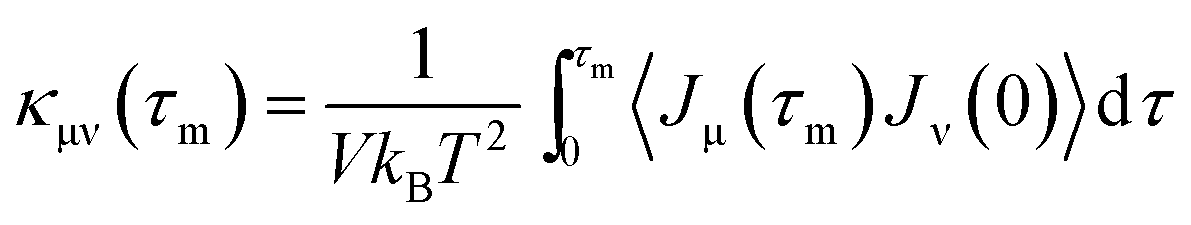
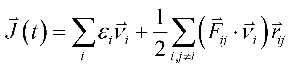
The structural and electronic properties of SNRs were studied by the projector augmented wave (PAW) potential26 within the framework of density functional theory (DFT). The code was implemented in the Vienna ab initio simulation package (VASP).27 The exchange-correlation energy was the form of Perdew–Burke–Ernzerhof (PBE)28 with a generalized gradient approximation (GGA). The plane wave cut-off energy of 500 eV and 11 × 1 × 1 Monkhorst–Pack k-points were set to ensure the total energies were well converged to be less than 1 × 10⁻⁶ eV and to ensure the maximum force on each atom was less than 0.02 eV Å−1. Standard supercell geometry was adopted so that SNRs were aligned in an orthogonal array. The closest distance between the ribbons concerned was set to be 12 Å so that they could be treated as independent entities. Based on the calculated band structures, the electronic transport coefficients were derived by using the semi-classical Boltzmann theory and relaxation time approximation.29 Within this method, the Seebeck coefficient (S) was independent of the relaxation time (τ), whereas the electrical conductivity (σ), the electronic component of thermal conductivity (κe), and the power factor (S2σ) were evaluated with respect to the parameter τ (S2σ/τ). The details of the relaxation time fitting are listed in the ESI.† The lattice thermal conductivity (κl) was predicted using equilibrium molecular dynamic (EMD) simulations combined with the Green–Kubo autocorrelation decay method.30–32 Based on the MD simulations, the lattice thermal conductivity κl can be predicted by using the Green–Kubo expression:here, 〈Jμ(τ)Jν(0)〉 is the heat current autocorrelation function, V is the volume of the simulation system, kB is the Boltzmann constant, and T is the system temperature. For a pair potential, the heat current J(τ) was expressed as
where εi is the site energy of the atom i, νi is the corresponding velocity, Fij and rij are the force and the separation between atoms i and j, respectively. The time step was chosen as 10 fs, and 500 ps raw heat current data were collected to calculate the heat current autocorrelation function.33
The thermal transport properties were calculated with the aid of the classical MD simulations, where suitable interatomic potentials were required. However, to the best of our knowledge, the empirical potential for the nanostructures of Sb were not available. Considering that the interatomic interactions in Sb NRs are mainly short range, we employed a simple two-body Morse potential, including the anharmonic interactions, which was found to predict the lattice thermal conductivity quite well.34 The Morse potential was in the form of φ(rij) = De[(1 − e−a(rij−r0))2 − 1], where De is the depth of the potential well, a is the measure of bond elasticity, rij is the interatomic separation between atoms i and j, and r0 is the equilibrium bond distance, which were determined by fitting the potential energy surface from first-principles calculations10,34,35 by utilizing the so-called GULP code.36 The energy surface was scanned by changing the periodic lengths along the ribbon axis to obtain a series of distinct configurations. The optimal parameters in the Morse potential are listed in Table S2.†
All systems were investigated by spin polarization and hydrogen-termination, and we found that reconstructed configurations are energetically more favorable than saturating the dangling bond with hydrogen atoms and spin polarization. Hence, only the non-spin polarized and reconstructed results are presented in the following discussion. The details are shown in Fig. S1 of ESI.†
Results and discussion
The one-atom-thick Sb sheet with identical Sb–Sb bond of 2.86 Å and ∠Sb–Sb–Sb angle of 91° is a single atomic layer that may be cut from bulk Sb (Fig. S2†); the energy per Sb atom is only 0.25 eV, which is higher than that of bulk Sb, suggesting its energetic stability. Subsequently, after cutting such a sheet along the armchair or zigzag path (Fig. S2b†), we can obtain armchair or zigzag Sb nanoribbons; they are denoted as ASNR-N (N = 1–12) or ZSNR-N (N = 1–6), following the notation for graphene nanoribbons,37 where N represents the ribbon width, and they are classified by the number of dimer lines or zigzag chains across the ribbon (Fig. 1a and b).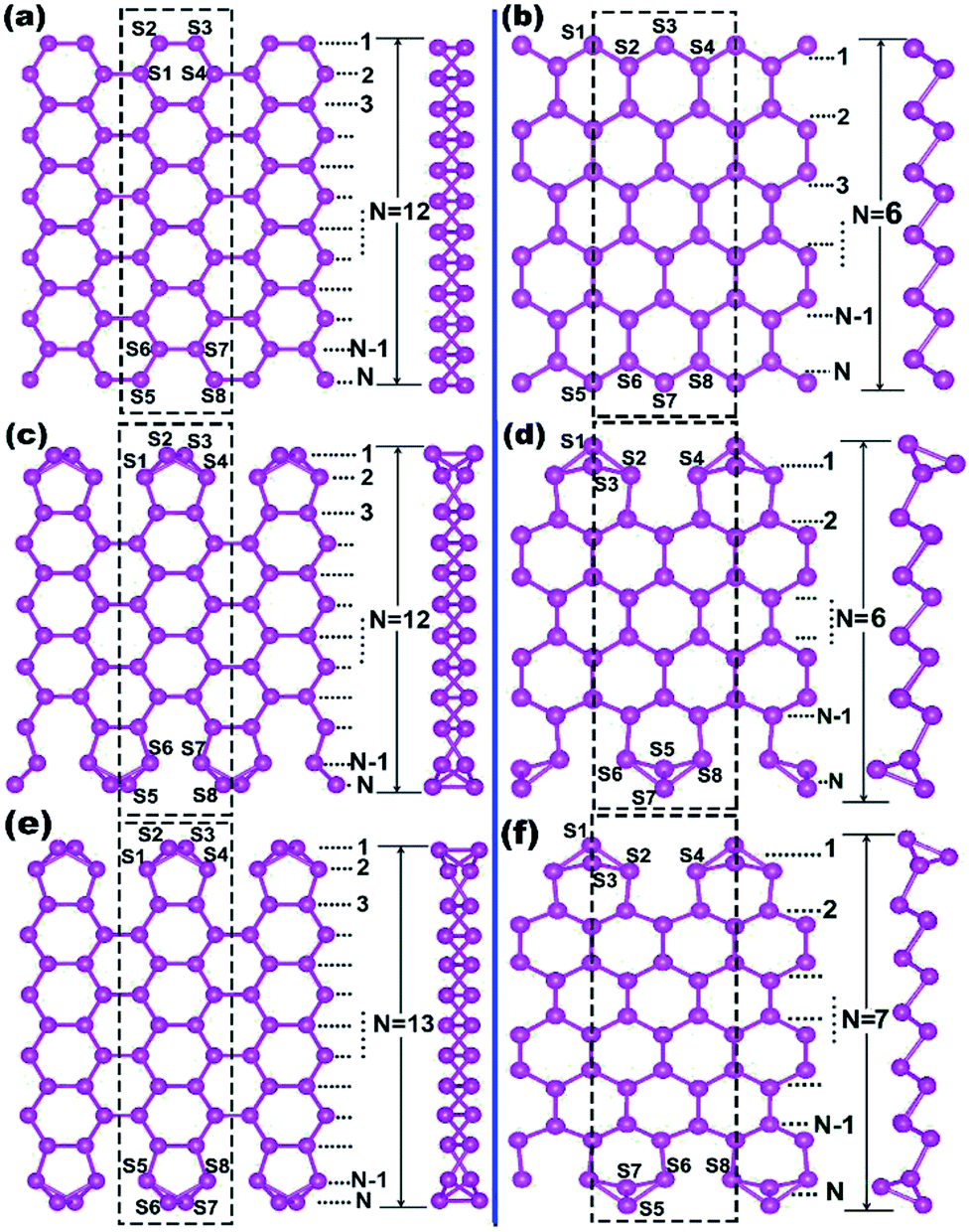 | ||
| Fig. 1 Top and side views of the structures of Sb nanoribbons: (a) the initial structure of ASNR-12, (b) the initial structure of ZSNR-6, (c) the fully relaxed structure of ASNR-recon-12, (d) the fully relaxed structure of ZSNR-recon-6, (e) the fully relaxed structure of ASNR-recon-13, (f) the fully relaxed structure of ZSNR-recon-7. Blank rectangles represent the 1 × 1 × 1 unit cell (building block) adopted in the calculation. The Sb atoms at each edge are numbered as Sn (n = 1–8). | ||
Upon structure relaxation, the initial ASNRs (Fig. 1a) undergo significant edge reconstructions, and the generated Sb ribbons are denoted as ASNR-recon. Taking ASNR-recon-12 (Fig. 1c) as an example, during structure relaxation, the Sb2 atom moves above and the Sb3 atom moves below the plane of the paper so as to form a third bond (or Sb2–Sb4 bond of 2.96 Å, Sb3–Sb1 = 2.96 Å), which is slightly longer than the Sb2–Sb3 = 2.86 Å bond. Consequently, all the dangling bonds at both edges are eliminated. Ribbons with different widths undergo different edge reconstructions: when N = even, the lower edge (Sb5–Sb6–Sb7–Sb8) is staggered with respect to the upper edge (Sb1–Sb2–Sb3–Sb4), as shown in ASNR-recon-12 (Fig. 1c); when N = odd, two edges are symmetrically arranged, as shown in ASNR-recon-13 (Fig. 1e). These observations are similar to those found for ABSNRs.24
On the contrary, after direct geometry relaxation (edge atoms has been not manually moved in the software), ZSNRs do not show significant edge reconstructions (denoted as ZSNR-unrecon-N), and all the dangling edge atoms still remain (Fig. S3†). Similarly, zigzag Bi nanoribbons are believed to undergo no edge reconstruction either.25 However, both unreconstructed ribbons of ZSNR-unrecon and ZBNR-unrecon25 are metallic (Fig. S3†) and are not desirable promising thermoelectric materials. This drives us to conduct a thorough study. To evaluate the stability of SNRs, the binding energy per atom (BE) and edge energy (EE)37,38 are calculated using the following equations, respectively:
| BE = (E(SNR) − N × E(Sbatom))/N | (1) |
| EE = (E(SNR) − N × E(Sb))/(2 × l) | (2) |
We note that unreconstructed ZSNRs still exhibit high binding energies (Fig. 2a, BEs vary with the width of ribbon from −3.68 to −3.80 eV per atom). Second, half of the edge Sb atoms (S1, S3, S5 and S7) are two-fold coordinated; they are still unsaturated with respect to the Sb atoms, which exhibit three-fold coordination. The binding interactions in bulk Sb are significantly lower than those in graphite (126 kJ mol−1 for Sb–Sb bond vs. 607 kJ mol−1 for C–C bond). Thus, we purposely break the Sb3–Sb4 bond in ZSNR-unrecon and move Sb3 toward Sb1 so as to form extra Sb3–Sb1 and Sb3–Sb4′ bonds (we call this a chemical-bond-driven edge reconstruction), which can eliminate all the dangling bonds of the edge Sb atoms. The geometry of such reconstructed ZSNRs (denoted as ZSNR-recon-N) was fully relaxed and converged to slightly longer Sb1–Sb2 = Sb2–Sb3 = 2.90 Å bonds and slightly shorter Sb1–Sb3 = 2.85 Å bonds (Fig. 1d and f). Unlike armchair ASNRs-recon, the zigzag ZSNRs-recon exhibit staggered edge configurations regardless of whether the width is even-numbered or odd-numbered (Fig. 1d and f). Our calculations also reveal that ZSNRs-recon with symmetric edge configurations have same phenomenon (Fig. S5†). To prove the stability of ZSNR-recon, we calculated the energy evolution of ZSNR-6 as an example (the result is shown in Fig. S6†). From the input structure to reconstruction, the binding energy (BE) first increases and then decreases to about −3.83 eV per atom. The no. 5 configuration has the highest energy compared with the others, indicating that this structure is quite unstable. However, the reconstructed-edge ribbon (no. 13) has the lowest binding energy among all of these conformations. However, this kind of ribbon is relatively unstable because the binding energies are slightly higher than those of staggered ones (Table S1†).
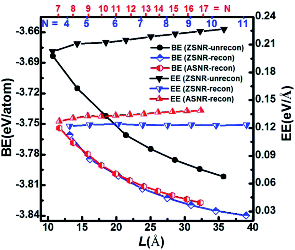 | ||
| Fig. 2 The calculated binding energies (BEs, in the unit of eV per Sb atom) and edge energies (EEs, in the unit of eV per Å) as a function of the ribbon width of the unreconstructed (black) and reconstructed (blue) ZSNRs, reconstructed ASNRs (red) and ZSNRs (blue). The top numbers represent the number of dimer lines in reconstructed ZSNRs (blue) and ASNRs (red). | ||
The plots of calculated BE and EE as a function of the width of Sb nanoribbons (L) are displayed in Fig. 2. Apparently, ZSNRs-recon considerably lowered the binding energies with decrease of about 0.05 eV per atom (0.11 eV per atom of FE) compared with the unconstructed ones (Fig. 2a). Therefore, the structure of such ZSNR-recon is not only rational, but also energetically more favourable. Fig. 2a shows that the binding energies of ZSNR-recon decrease with increasing ribbon width. Similar characteristics could be found for the formation energy, as shown in Fig. S4.† This is important evidence for the stability and rationality of ZSNR-recon. From Fig. 2a, we find that the edge atoms dominate the binding energy; yet, the edge energy EE is nearly independent of the ribbon width. Fig. S3b† illustrates that FEs of both ASNR-recon and ZSNR-recon depend on the width and vary in the ranges of 0.06–0.13 and 0.04–0.12 eV per atom, respectively. These values are much smaller than the values (0.2–0.4 eV per atom) of GNRs.38 We believe that buckled structures and edge reconstruction facilitate better release of the extra elastic energy than the planar structures of GNRs, eventually leading to smaller FEs in SNRs. Furthermore, the edge energies of SNRs are one order of magnitude lower than those of GNRs.39,40 With increasing ribbon width, EE increases linearly for ASNR-recon but barely increases for ZSNR-recon. The edge reconstruction motifs of ZSNR-recon are located in the upper and lower portions of the ribbon plane (Fig. 1), which is a good balance for the force of the edge atom bending to the center; thus, the EE value is relatively lower than that for ASNRs-recon and independent of the width.
The calculated band structures of ASNRs-recon reveal that all ASNRs-recon samples considered are semiconducting with band gaps of ca. 0.75–0.90 eV (Fig. 3). From N = 7 to 17, the highest two valence bands (VBs) of ASNRs-recon-N gradually converge because the energy separation between A and B bands decreases and a convergence is reached at N > 15 (Fig. S7†). However, the lowest two conduction bands (CBs) are degenerate for the even-numbered ASNRs-recon only (Fig. 3a and S7†). As a result, the calculated band gaps of ASNRs-recon exhibit a width-dependent odd–even oscillation that ends at N = 17 with a band gap of ca. 0.88 eV. Such a band-gap oscillation is similar to that found in pristine BiSb armchair nanoribbons24 but is quite different from that observed for graphene nanoribbons (GNRs).38
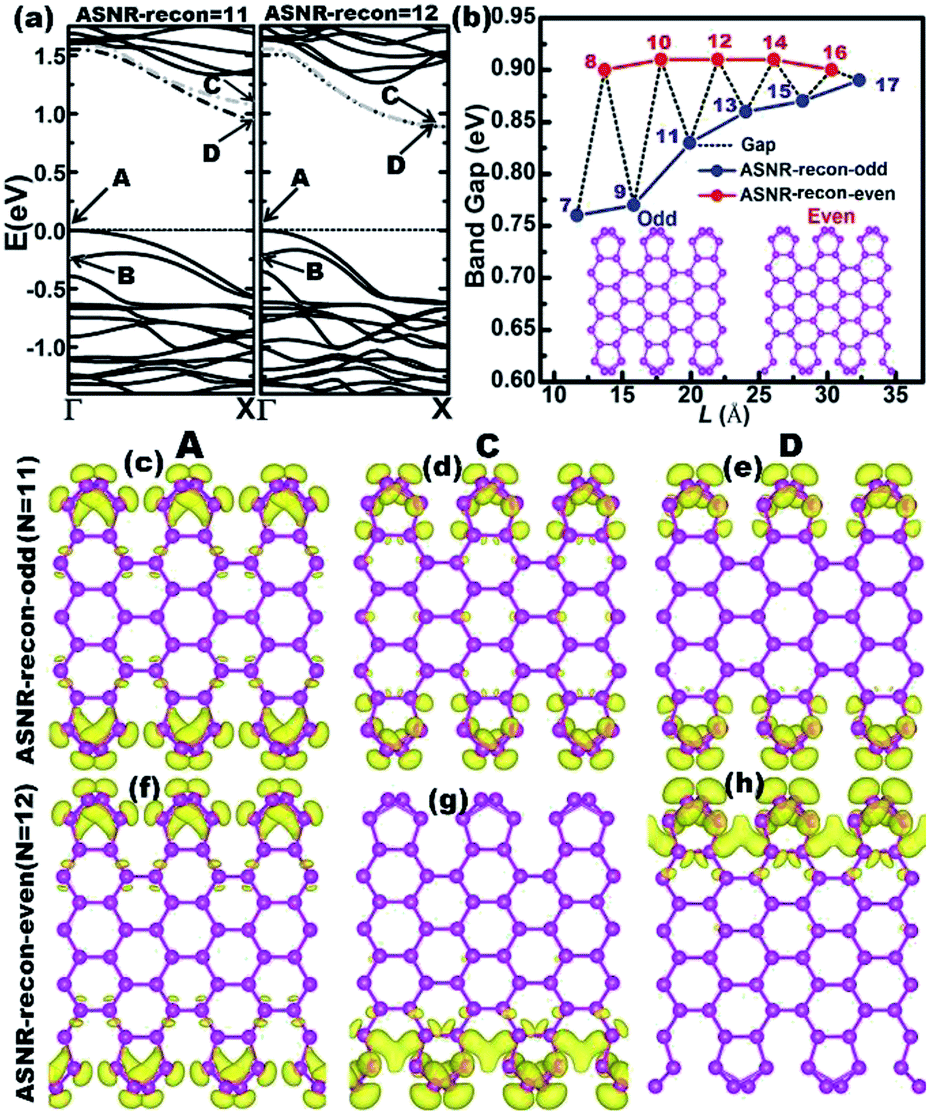 | ||
| Fig. 3 (a) The band structures of ASNR-recon-11 and -12; (b) the calculated band gap as a function of width of ASNRs-recon. The insets show the fully relaxed structures of odd- (left) and even-numbered (right) ASNR. The numbers depicted inside represent the number of dimer lines; (c–h) the band-decomposed charge densities of VBM, CBM, and conduction band at the X point of ASNR-recon-11 (c–e) and -12 (f–h). The density of isosurfaces (displayed by yellow pixels) is 1.5 × 10⁻³ e Å−3. | ||
The band-decomposed charge densities of the VBM and CBM of ASNR-recon are shown in Fig. 3c–h and S8.† Clearly, the charge densities are mainly contributed by the edge atoms and sharply decay toward the center of the Sb atoms. Meanwhile, the partial charge densities of the two doubly degenerate at the X-point are distributed around the two edges of ASNRs-recon-even. The reconstructed motifs, staggered at both edges of ASNRs-recon-even, interact tightly between the two edges mediated by the interior Sb atoms. For ASNRs-recon-odd, their two reconstructed motifs at opposite edges in a unit cell appear as independent building blocks, and the interaction between the building blocks is much weaker since very few electron densities distribute around the bonds connecting the two building blocks. In particular, this influence on the band gap is more significant for ASNRs-recon-odd with narrower widths. For example, in ASNR-recon-7 or ASNR-recon-9 (Fig. S8†), the building blocks are connected through only one or two Sb–Sb bonds, respectively. Then, the edge influence on the band gaps becomes smaller and smaller with increasing ribbon width, which is manifested by the indirect gaps of both ASNRs-recon-odd and ASNRs-recon-even approaching a plateau.
Up to now, the intrinsic reason behind such oscillation remains unknown. From Fig. 3c–h and S7,† we see that only one side of the nanoribbon contributes to the CBM of ASNRs-recon-12, -14 and -16. This suggests that the reconstructed atoms at the two edges have no interactions.24 In other words, the symmetric edge configurations facilitate the interactions of the atoms at the two edges, through which the CBM is split into a C band and a lower-energy D band. Such a lower-energy D band narrows the band gap (Fig. 3a and S8†). However, for the even-numbered ASNRs, C and D bands are degenerate; thus, the band gaps remain wide and are systematically larger than those of the odd-numbered ones, especially for the narrower ribbons. Additionally, the band gap oscillation gradually vanishes with increasing ribbon width and finally approaches a constant value when N > 17 (Fig. 3b).
Conversely, the calculated band gaps of ZSNRs-recon are about 1.2 eV and are nearly independent of the width (Fig. 4b and S9†). This coincides with the width independence of the EE values of ZSNRs-recon, as shown in Fig. 2b. As mentioned earlier in ASNR-recon, the edge reconstruction motifs of ZSNR-recon are also staggered at both sides even when the ribbons have odd or even zigzag paths. Both sides are tightly connected together by intermediate atoms, and a similar phenomenon can be found in ASNRs-recon-even.
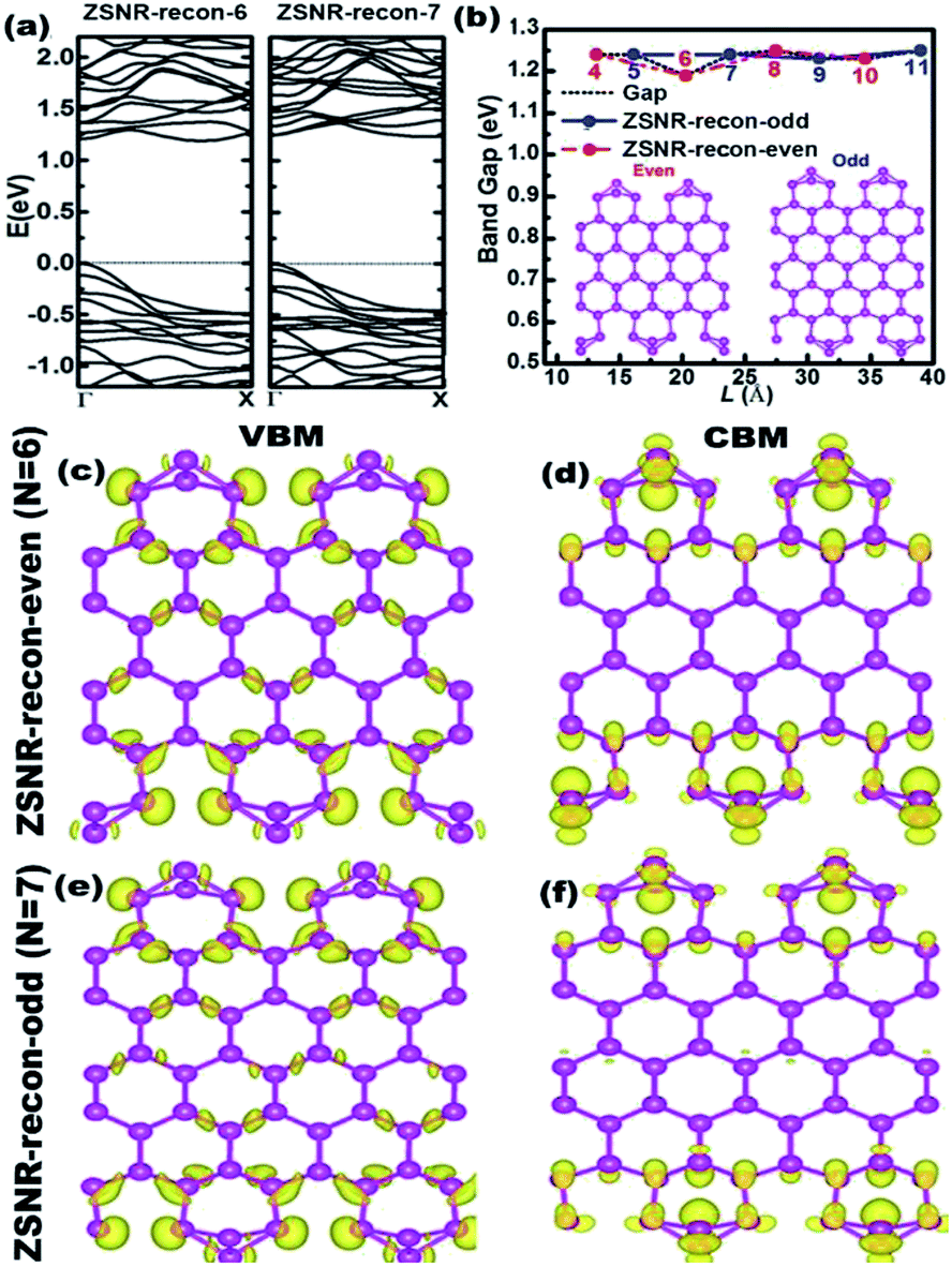 | ||
| Fig. 4 (a) The band structures of ZSNR-recon-6 and -7; (b) the calculated band gap as a function of width of ZSNRs-recon. The insets show the fully relaxed structures of even- (left) and odd-numbered (right) ZSNR. The numbers depicted inside represent the number of zigzag chains; (c–f) the band-decomposed charge densities of VBM, CBM for ZSNR-recon-6 (c and d) and −7 (e and f). The density of isosurfaces (displayed by yellow pixels) is 1.5 × 10⁻³ e Å−3. | ||
The calculated lattice thermal conductivities are shown in Fig. S10.† The lattice thermal conductivities are 0.7–1.1 and 0.2–0.4 W m−1 K−1 for ASNRs-recon and ZSNRs-recon, respectively. These values are considerably lower than that of metallic bulk Sb (the thermal conductivity is about 24 W m−1 K−1 and electrical resistivity is 417 nΩ m for Sb at 300 K in ref. 42, according to the Wiedemann–Franz law, the lattice thermal conductivity of bulk Sb is about 7 W m−1 K−1 at 300 K), whereas those of the unreconstructed zigzag nanoribbons (ZSNRs-unrecon) are remarkably high. For example, the lattice thermal conductivity of ZSNR-unrecon-4 is calculated to be about 2 W m−1 K−1, which is 100% or 400% higher than those of ASNR- and ZSNR-recon. As the ribbon width increases, the lattice thermal conductivity increases nearly linearly, which is in agreement with those found in other materials.41,43,44 From Fig. S10,† we see that the lattice thermal conductivities of ASNR-recon are larger than those of ZSNRs-recon. After further analysis, we found that the thermal conductivity has a certain relationship with the density of atom per unit length (N/L) along the dimer line or the zigzag chain (Fig. S10b†). Apparently, N/L of ASNRs-recon (about 0.55 Å−1) is higher than that of ZSNRs-recon (about 0.48 Å−1). This indicates that the denser atomic arrangement in the former benefits the thermal transport more and gives rise to larger lattice thermal conductivity. This result further confirms that the chemical-bond-driven edge reconstruction is necessary to improve the thermoelectric properties of zigzag Sb nanoribbons.
Transport properties as a function of width are displayed in Fig. 5 for ASNRs- and ZSNRs-recon at 300 K with τ = 1.3 × 10⁻¹³ s (τ fitted with bulk Sb, as shown in Fig. S11†). As we know, n-type material is electron-dominated; thus, the transport properties, including Seebeck coefficient S and electrical conductivity σ, should be mainly determined by CBs near EF. This is demonstrated in the odd–even oscillation band gap (Fig. 3) of ASNRs-recon, which is mostly influenced by CBs (Fig. S8†). Consequently, the n-type ASNRs-recon sample exhibits odd–even oscillations in both S (Fig. 5a) and σ (Fig. 5c). On the other hand, transport properties of p-type ribbons are mainly decided by VBs near EF. Thus, p-type ASNRs-recon do not show any odd–even oscillation of S and σ (Fig. 5a and c), which coincides with their electronic structures plotted in Fig. S7 and S8.† The n-type ASNRs-recon-even have larger σ than -odd ones because the stronger edge interactions in the former benefit electron transport (Fig. 5c). Meanwhile, σ of ASNRs-recon is almost 10 times larger than those of ZSNRs-recon (Fig. 5c vs. d). The S values of ASNRs-recon fall in the range of 240–320 μV K−1 and are systematically larger than those of ZSNRs-recon (Fig. 5a vs. b).
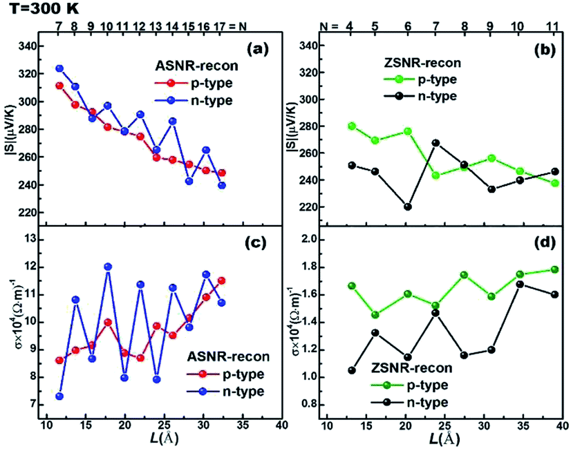 | ||
| Fig. 5 The calculated absolute values of the Seebeck coefficient |S| of (a) ASNRs-recon; (b) ZSNRs-recon; and electrical conductivity σ with τ = 1.3 × 10⁻¹³ s at 300 K of (c) ASNRs-recon; (d) ZSNRs-recon. The optimal carrier concentrations are chosen. The top numbers represent the number of dimer lines or zigzag chains. | ||
In addition, for each ribbon, the optimal carrier concentration at 300 K has been predicted in Fig. 6; “optimal” means to optimize the ZT value. The calculation results reveal that the optimal carrier concentrations of ASNRs-recon-odd are in the range between 1018 and 1020 cm−3, and the maximum ZT (ZTmax) values can vary between 0.75 and 1.81 as a function of the ribbon width. ASNRs-recon-even can realize better ZTmax values from 0.86 to 1.91 (Fig. 6a–d). In the case of ZSNRs-recon, the optimal carrier concentrations are in the ranges of 1019–1020 cm−3 and 1018–1020 cm−3 for n- and p-type materials, with which ZTmax of 1.2 may be reached (Fig. 6e–h). These results demonstrate that the studied Sb nanoribbons are promising TE materials for room-temperature applications; the ZT values of these structures, as shown in Fig. 6, are remarkably higher than 0.54 of Bi1−xSbx nanoalloys12 and 0.28 of Ho-doped Bi0.88Sb0.12,45 and they are comparable to 0.8 of doped CsBi4Te6 (at 225 K)2 and 0.9 of Bi2−xSbxTe3−ySey alloys (at 310 K).46
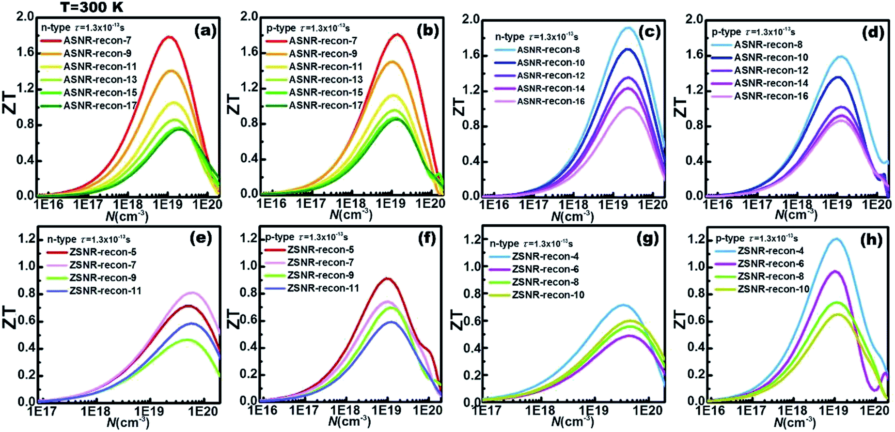 | ||
| Fig. 6 The calculated ZT values as a function of the carrier concentration with τ = 1.3 × 10⁻¹³ s at 300 K for (a and b) ASNRs-recon-odd; (c and d) ASNRs-recon-even; (e and f) ZSNRs-recon-odd; (g and h) ZSNRs-recon-even. | ||
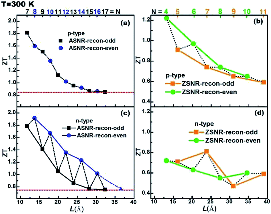
The ZT value dependence on the ribbon width is also studied, as shown in Fig. 7. For p-type ASNRs-recon, ZT increases from 0.8 to 1.8 with decreasing ribbon width (Fig. 7a). However, for n-type ASNRs-recon shown in Fig. 7c, the ZT value exhibits odd–even oscillation on the width, which is consistent with the oscillation of the conduction bands shown in Fig. 3b. For p-type ZSNRs-recon, the slightly change ZT–width curve (Fig. 7b) also reflects the behavior of the valence band near EF (Fig. 4). For example, n-type ASNR-recon-8 can realize ZT = 1.91 at 300 K, which is ca. 100 times that of thin Sb films.20 Moreover, the highest ZT values of ZSNRs-recon are 1.22 for p-type ZSNR-recon-4 and 0.81 for n-type ZSNR-recon-7. Both n- and p-type ASNRs-recon-7 exhibit a very high ZT value of 1.8. Even the wider ASNR-recon-17 sample (with a width of 35 Å) still shows high ZT of 0.8. In general, the ASNR-recon sample shows better TE performance than ZSNRs-recon.
 | ||
| Fig. 7 The calculated ZT values as a function of the ribbon width (with τ = 1.3 × 10⁻¹³ s): (a and c) ASNRs-recon; (b and d) ZSNRs-recon. The top numbers represent the number of dimer lines or zigzag chains. | ||
Conclusions
In summary, our first-principles calculations suggest that one-atom-thick Sb nanoribbons exhibit excellent structural and electronic properties that are closely related to the ribbon width and chirality. We observe that the edge reconstruction is the key to realize the conversion of metal to semiconductor for these ribbons. Previous studies on BiSb24 and Bi nanoribbons25 concluded that a “zigzag” nanoribbon will not undergo any edge reconstruction and will remain metallic. Herein, we illustrate that chemical-bond-driven edge reconstruction of ZSNRs is energetically favorable and helps to stabilize the whole structure. In addition, we reveal that the odd–even oscillation of band gaps of ASNRs originates from the atomic interactions at the edge, which determines the behaviors of the VB top and CB bottom and consequently leads to odd–even oscillations of the absolute values of S, σ and ZT. These transport properties have been evaluated using Boltzmann theory calculations. Furthermore, the lattice thermal conductivities are investigated by the equilibrium molecular dynamic simulations combined with the Green–Kubo formalism. Our results reveal that n-type ASNR-recon-8 can show ZT = 1.91 at 300 K, which is about 100 times that of the thin Sb film,20 whereas p-type ZSNR-recon can exhibit ZT = 1.22 at 300 K. Our theoretical studies suggest that Sb nanoribbons may be promising room-temperature high-performance thermoelectric materials and can have potential applications in size minimization of electronic devices. Additionally, the concept of the chemical-bond-driven edge reconstruction may be useful for related systems.Conflicts of interest
There are no conflicts to declare.Acknowledgements
This work was supported by the National Natural Science Foundation of China (Grants 51702053), the Educational Research Foundation for Middle-aged and Young Scientist by Educational Commission of Fujian Province of China (JAT160072), and the Open Project Program of the State Key Laboratory of Photocatalysis on Energy and Environment (SKLPEE-KF201717).Notes and references
- M. Scheele, N. Oeschler, I. Veremchuk, K.-G. Reinsberg, A. Kreuziger, A. Kornowski, J. Broekaert, C. Klinke and H. Weller, ACS Nano, 2010, 4, 4283 CrossRef CAS PubMed.
- D.-Y. Chung, T. Hogan, P. Brazis, M. Rocci-Lane, C. Kannewurf, M. Bastea, C. Uher and M. G. Kanatzidis, Science, 2000, 287, 1024 CrossRef CAS PubMed.
- Y. Q. Cao, X. B. Zhao, X. B. Zhu and J. P. Tu, Appl. Phys. Lett., 2008, 92, 143106 CrossRef.
- J. P. Heremans, C. M. Thrush, D. T. Morelli and M.-C. Wu, Phys. Rev. Lett., 2002, 88, 216801 CrossRef PubMed.
- Y. Sun, H. Cheng, S. Gao, Q. Liu, Z. Sun, C. Xiao, C. Wu, S. Wei and Y. Xie, J. Am. Chem. Soc., 2012, 134, 20294 CrossRef CAS PubMed.
- Y. Lan, B. Poudel, Y. Ma, D. Wang, M. S. Dresselhaus, G. Chen and Z. Ren, Nano Lett., 2009, 9, 1419 CrossRef CAS PubMed.
- Y.-M. Lin, X. Z. Sun and M. S. Dresselhaus, Phys. Rev. B: Condens. Matter Mater. Phys., 2000, 62, 4610 CrossRef CAS.
- E. Shapira, A. Holtzman, D. Marchak and Y. Selzer, Nano Lett., 2012, 12, 808 CrossRef CAS PubMed.
- G. Wang, L. Endicott and C. Uher, Sci. Adv. Mater., 2011, 3, 539 CrossRef CAS.
- P. Ghaemi, R. S. K. Mong and J. E. Moore, Phys. Rev. Lett., 2010, 105, 166603 CrossRef PubMed.
- H. Y. Lv, H. J. Liu, L. Pan, Y. W. Wen, X. J. Tan, J. Shi and X. F. Tang, J. Phys. Chem. C, 2010, 114, 21234 CrossRef CAS.
- B. Landschreiber, E. Güneş, G. Homm, C. Will, P. Tomeš, C. Rohner, A. Sesselmann, P. J. Klar, S. Paschen, E. Müller and S. Schlecht, J. Electron. Mater., 2013, 42, 2356 CrossRef CAS.
- L. R. Windmiller, Phys. Rev., 1966, 149, 472 CrossRef CAS.
- J. Heremans, C. M. Thrush, Y.-M. Lin, S. B. Cronin and M. S. Dresselhaus, Phys. Rev. B: Condens. Matter Mater. Phys., 2001, 63, 085406 CrossRef.
- X.-S. Wang, S. S. Kushvaha, Z. Yan and W. Xiao, Appl. Phys. Lett., 2006, 88, 233105 CrossRef.
- Y. Zhang, L. Li, G. H. Li and L. D. Zhang, Phys. Rev. B: Condens. Matter Mater. Phys., 2006, 73, 113403 CrossRef.
- H. Hu, M. Mo, B. Yang, M. Shao, S. Zhang, Q. Li and Y. Qian, New J. Chem., 2003, 27, 1161 RSC.
- L. Li, Y. Xiao, Y. Yang, X. Huang, G. Li and L. Zhang, Chem. Lett., 2005, 34, 930 CrossRef CAS.
- M. Zhang, Z. Wang, G. Xi, D. Ma, R. Zhang and Y. Qian, J. Cryst. Growth, 2004, 268, 215 CrossRef CAS.
- F. Völklein and E. Kessler, Phys. Status Solidi B, 1990, 158, 521 CrossRef.
- J. H. Xu and C. S. Ting, Appl. Phys. Lett., 1993, 63, 129 CrossRef CAS.
- F. Ma, Z. Guo, K. Xu and P. K. Chu, Solid State Commun., 2012, 152, 1089 CrossRef CAS.
- U. Treske, F. Ortmann, B. Oetzel, K. Hannewald and F. Bechstedt, Phys. Status Solidi A, 2010, 207, 304 CrossRef CAS.
- H. Y. Lv, H. J. Liu, X. J. Tan, L. Pan, Y. W. Wen, J. Shi and X. F. Tang, Nanoscale, 2012, 4, 511 RSC.
- L. Zhu, T. Zhang and J. Wang, J. Phys. Chem. C, 2010, 114, 19289 CrossRef CAS.
- P. E. Blöchl, Phys. Rev. B: Condens. Matter Mater. Phys., 1994, 50, 17953 CrossRef.
- G. Kresse and J. Furthmüller, Phys. Rev. B: Condens. Matter Mater. Phys., 1996, 54, 11169 CrossRef CAS.
- J. P. Perdew, K. Burke and M. Ernzerhof, Phys. Rev. Lett., 1996, 77, 3865 CrossRef CAS PubMed.
- G. K. H. Madsen and D. J. Singh, Comput. Phys. Commun., 2006, 175, 67 CrossRef CAS.
- R. Kubo, M. Toda and N. Hashitsume, Statistical Physics II: Nonequilibrium statistical mechanics, Springer-Verlag, Berlin, 1991 Search PubMed.
- J. Dong, O. F. Sankey and C. W. Myles, Phys. Rev. Lett., 2001, 86, 2361 CrossRef CAS PubMed.
- P. K. Schelling, S. R. Phillpot and P. Keblinski, Phys. Rev. B: Condens. Matter Mater. Phys., 2002, 65, 144306 CrossRef.
- We checked the finite-size effect by repeating the simulations with different number of atoms. Take the ASNR-recon-12 for example; the numbers of atoms are 220, 440, 880, and 1100. Periodic boundary conditions were imposed. The thermal conductivity of ASNR-recon-12 at 300 K is converged even when the smallest size is considered (N = 220), as shown in Fig. S11.† Conservatively, we chose N = 440 for simulation of the lattice thermal conductivity of ASNR-recon-12. Fig. S13† shows the normalized heat current autocorrelation function ASNR-recon-12 with 440 Sb atoms at 300 K; g(t) has rapidly oscillating terms with an exponential envelope. The heat current autocorrelation function rapidly drops from unity to a value near zero at 50 ps.
- B. Qiu and X. L. Ruan, Phys. Rev. B: Condens. Matter Mater. Phys., 2009, 80, 165203 CrossRef.
- N. A. Katcho, N. Mingo and D. A. Broido, Phys. Rev. B: Condens. Matter Mater. Phys., 2012, 85, 115208 CrossRef.
- J. D. Gale, J. Chem. Soc., Faraday Trans., 1997, 93, 629 RSC.
- Y. W. Son, M. L. Cohen and S. G. Louie, Phys. Rev. Lett., 2006, 97, 216803 CrossRef PubMed.
- B. Huang, H. Lee, B. L. Gu, F. Liu and W. Duan, Nano Res., 2011, 5, 62 CrossRef.
- C. K. Gan and D. J. Srolovitz, Phys. Rev. B: Condens. Matter Mater. Phys., 2010, 81, 125445 CrossRef.
- A. I. Boukai, Y. Bunimovich, J. Tahir-Kheli, J.-K. Yu, W. A. Goddard III and J. R. Heath, Nature, 2008, 451, 168 CrossRef CAS PubMed.
- C. Kittel, Introduction to Solid State Physics, Wiley, New York, 7th edn, 1996 Search PubMed.
- V. Barone, O. Hod and G. E. Scuseria, Nano Lett., 2006, 6, 2748 CrossRef CAS PubMed.
- D. Donadio and G. Galli, Phys. Rev. Lett., 2009, 102, 195901 CrossRef PubMed.
- H. Sevinçli and G. Cuniberti, Phys. Rev. B: Condens. Matter Mater. Phys., 2010, 81, 113401 CrossRef.
- K. C. Lukas, G. Joshi, K. Modic and Z. F. Ren, J. Mater. Sci., 2012, 47, 5729 CrossRef CAS.
- L. N. Luk'yanova, V. A. Kutasov, P. P. Konstantinov and V. V. Popov, Phys. Solid State, 2010, 52, 1599 CrossRef.
Footnotes |
| † Electronic supplementary information (ESI) available. See DOI: 10.1039/c8ra07395c |
| ‡ These authors contributed equally to this work. |
| This journal is © The Royal Society of Chemistry 2019 |