DOI:
10.1039/C9QM00017H
(Research Article)
Mater. Chem. Front., 2019,
3, 640-649
Precise regulation of the emissive layer for ultra-high performance white organic light-emitting diodes in an exciplex forming co-host system†
Received
11th January 2019
, Accepted 8th February 2019
First published on 12th February 2019
Abstract
Nowadays, white organic light-emitting diodes (WOLEDs) have attracted more attention in solid-state lighting due to their merits of low power consumption, flat shadowless illumination, soft and weak blue light, flexible emission and so on. Regrettably, it is still an extremely challenging subject to achieve ultra-efficient WOLEDs exceeding 100 lm W−1. In this paper, we present a general approach to achieve low turn-on voltage (∼2.4 V), ultra-high efficiency WOLEDs based on an exciplex forming co-host system. The key to our design strategy is the precise management of the phosphor dopant concentration and the reasonable arrangement of the emissive layers to efficiently solve the trade-off between charge carrier trapping and energy transfer in electroluminescence (EL) processes. The resulting WOLEDs realize a forward-viewing maximum power efficiency and external quantum efficiency of 106.4 lm W−1 and 23.5%, 69.9 lm W−1 and 23.4%, respectively, for complementary-color and three-color WOLEDs. The EQEs retain over 22% at 1000 cd m−2, exhibiting extremely low efficiency roll-off. Such outstanding device performance and ultra-high efficiencies should be attributed to the enhancement of energy transfer and the reduction of charge carrier trapping in the exciplex co-host system. These findings will be conducive to enhancing the efficiency of WOLEDs, and promoting industrial development in lighting markets.
Introduction
With the rapidly increasing worldwide demand for illumination, the solid-state lighting (SSL) industry, as one of the important means of achieving environmentally friendly and sustainable development goals of social and economic significance, has ushered in a new period of development. SSL sources include light-emitting diodes (LEDs) and organic light-emitting diodes (OLEDs). By comparison with LEDs, OLEDs have more excellent advantages, such as flat shadowless emission, low cost, low weight, ultrathin size, easy flexibility, large area, lower power consumption and homogenous illumination etc.1–5 In this respect, OLEDs have shown particularly promising potential for resource-conserving lighting technologies, whilst the development of OLEDs has been in progress for more than 30 years. Due to their eye-friendly soft light, WOLEDs are urgently desired to become new generation SSL sources in the lighting market. Although enormous efforts have been carried out to improve the efficiency of WOLEDs, a few power efficiencies (PEs) of the resulting WOLEDs have surpassed that of fluorescent lamps (70–90 lm W−1) if there are no optical out-coupling structures.6–12 Therefore, it is still an extremely challenging subject to realize the forward-viewing PE of WOLEDs beyond 100 lm W−1 without using a light out-coupling technique.
Compared with fluorescent emitters, phosphorescent emitters have unparalleled characteristics to realize high PE, which can harvest effectively both singlet and triplet excitons simultaneously and thus realize 100% internal quantum efficiency (IQE), making complete use of the electrogenerated excitons.2,13,14 As is known, the phosphors are generally doped in a proper host to realize high efficiency OLEDs. For such phosphor-doped OLEDs, there are two electroluminescence (EL) mechanisms by either direct charge carrier trapping on the dopant or host–dopant energy transfer. Thus the doping concentrations and the location of phosphorescent dopants in the corresponding host materials may inevitably alter the carrier injection, transport, and recombination process in the emissive layer (EML), which could have a substantial influence on the EL performance of the OLEDs.15–24 For instance, Forrest's group demonstrated a long lifetime blue OLED by using a graded dopant concentration profile in the EML.21,22 Liu et al. found that phosphorescent dopants could be used to directly assist transport carriers, thus achieving a series of high efficiency monochrome OLEDs.19 Zhu et al. took advantage of the effect of red and green dopants on charge carrier transport to design different EML structures with red-blue-green and green-blue-red sequences for high efficiency WOLEDs.23 Wang et al. illustrated that orange phosphorescent dopant (bis(2-(9,9-diethyl-9H-fluoren-2-yl)-1-phenyl-1H-benzoimidazol-N,C3)iridium(acetylacetonate)) could broaden the exciton recombination zone and enhance the efficiency by utilizing its electron-transporting and hole-trapping features.24
In recent years, exciplex systems formed between suitable donor and acceptor molecules have been rapidly developed in OLEDs, especially for serving as phosphorescent hosts due to these advantages, such as bipolar carrier transport, broad recombination zone and low driving voltage.17,25–29 Recently, lots of monochrome OLEDs based on different exciplex hosts with high external quantum efficiency (EQE) of approximately 30% have been achieved.17,30–33 As for all phosphorescent WOLEDs, it is still one of the most challenging tasks that there are limited reports of high efficiency WOLEDs based on exciplex hosts, and the systematic study of the effects of the charge carrier trapping on EL performance of the fabricated all phosphorescence WOLEDs based on exciplex hosts have been scarcely reported.
In this paper, we have not only demonstrated the influence of charge carrier trapping on EL performance, but also achieved ultra-high efficiency WOLEDs by the subtle manipulation of the location and concentration of the phosphorescent dopants in the EML. The resulting complementary-color WOLEDs have achieved excellent EL efficiencies with the forward-viewing maximum PE and EQE of 106.4 lm W−1 and 23.5%, respectively, which should be one of the highest values for WOLEDs without using out-coupling enhancement techniques to date. The resulting three-color WOLED also exhibits maximum efficiencies of 69.6 lm W−1 and 23.4%.
Experimental section
Materials
ITO is indium tin oxide acting as the anode. HAT-CN is 1,4,5,8,9,11-hexaazatriphenylene-hexacarbonitrile acting as the hole injection layer. TAPC is 1-bis[4-[N,N-di(4-tolyl)amino]phenyl]-cyclohexane acting as the hole transport layer. TCTA is 4,4,4-tris(N-carbazolyl)triphenylamine. mCBP is 9,9′-biphenyl-3,3′-diylbis-9H-carbazole acting as the electron donor in the exciplex system. PO-T2T is (1,3,5-triazine-2,4,6-triyl)-tris(benzene-3,1-diyl)tris(diphenyl-phosphineoxide) acting as the electron transport layer and electron acceptor in the exciplex system. Liq is 8-hydroxyquinolatolithium serving as the buffer layers for electron injection. Al is the cathode. Iridium(III)bis(4-(4-t-butylphenyl)thieno[3,2-c]pyridinato-N,C2)acetylacetonate (Ir(tptpy)2acac), bis(2-phenylpyridine)iridium(III) (Ir(ppy)2acac) and iridium(III)bis[(4,6-difluorophenyl)-pyridinato-N,C2′]picolinate (FIrpic) served as the orange, green and blue phosphorescent dopants, respectively. All of these materials were used as commercially purchased without further purification.
Photoluminescence (PL) characterization
All of the films prepared using vacuum evaporation on quartz substrates were studied using a Shimadzu UV-2600 spectrophotometer for the UV-vis absorption spectra. The PL spectra were recorded with a fluorospectrophotometer (Edinburgh FL980). The measurement of the transient PL spectra was carried out on a Quantaurus-Tau fluorescence lifetime measurement system (C11367-03, Hamamatsu Photonics Co.).
OLED fabrication and characterization
The OLEDs were prepared by evaporating each layer onto the ITO substrate sequentially at pressures below 1 × 10⁻⁴ Pa. Before transferring to a deposition chamber, the ITO substrates were cleaned with ultra-sonication in detergents and deionized water, dried in an oven at 120 °C for 1 h, and finally subjected to oxygen plasma treatment for 6 min. Then, HAT-CN was deposited at 0.05 nm s−1. The vacuum evaporation rates of other organic materials were 0.1–0.15 nm s−1. Finally, a 1.5 nm-thick layer of Liq was deposited at 0.03 nm s−1 and a metallic cathode (Al) 150 nm thick was deposited at a rate of 0.5–0.8 nm s−1. The effective emission area of the devices is 4 × 4 mm2. All the OLEDs were tested without encapsulation at room temperature under atmospheric conditions. The current density–voltage–luminance (J–V–L) characteristics were evaluated with a Keithley 2400 source meter and a LS110 luminance meter. The electroluminescence (EL) spectra were measured using a spectrascan PR650 spectrophotometer. The EQEs were calculated from the luminance, current density and EL spectrums with the hypothesis of Lambertian distribution.
Results and discussion
Design concept of WOLEDs
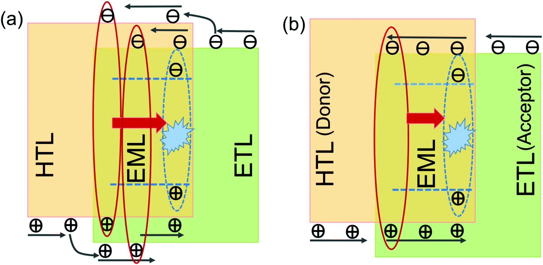
The configuration of the fabricated WOLEDs in our study is ITO/HAT-CN (15 nm)/TAPC (60 nm)/TCTA (5 nm)/mCBP (5 nm)/EMLs (18 nm)/PO-T2T (45 nm)/Liq (1.5 nm)/Al (150 nm). The energy levels of the organic molecules used in our devices are depicted in Fig. S1 (ESI†). In order to guarantee the development of high-performance WOLEDs, several strategies were adopted in our devices. As depicted in Fig. 1, there are two paths to form excitons at the dopant molecules in the co-host system formed by mixing the hole transporting material (HTM) and the electron transporting material (ETM): (1) direct charge trapping by the dopants, or (2) the holes are transported from the HTM to the ETM over the energy barrier to form an exciton at the ETM (or the electrons are transported from the ETM to the HTM over the energy barrier to form exciton at the HTM), and then the excitons transfer to the dopants. Both mechanisms would increase the operating voltage. However, in the exciplex forming co-host system, a low operating voltage can be achieved because charge carriers reach the EML without energy barriers to form stable, lower exciplex energy state excitons. Thus, we adopted an exciplex (mCBP:PO-T2T) as the host for phosphorescent dopants. This exciplex with blue emission has a triplet energy level (T1) of 2.63 eV, which is higher than those of phosphorescent dopants FIrpic (2.62 eV) and Ir(tptpy)2acac (2.2 eV), maintaining effective exothermic energy transfer from host to guest.32 Furthermore, the T1 values of the exciplex donor (mCBP) and accepter (PO-T2T) are higher than that of the exciplex for efficient exciton confinement within EMLs. Besides, PO-T2T served as the electron-transporting layer with high electron mobility, which guarantees barrier-free electron injection into the EMLs. Due to the deep HOMO energy level of 7.5 eV, PO-T2T also displays hole-blocking properties. The high hole mobility of TAPC, and the stepped progression of the HOMO energy levels of TAPC, TCTA and mCBP are beneficial for effectively transporting holes and lowering the operating voltage. Lastly, a multi-EML structure would provide a more reliable platform for flexible manipulation of each EML as well as precise management of the charge and exciton distribution within the EMLs.2,9,34
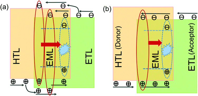 |
| | Fig. 1 (a) Schematic diagram of charge carrier transport and combination explaining the difference between (a) a co-host system with non-exciplex and (b) exciplex forming co-host based devices. HTL, EML and ETL represent hole transporting layer, emissive layer and electron transporting layer, respectively. | |
EL performance of WOLEDs
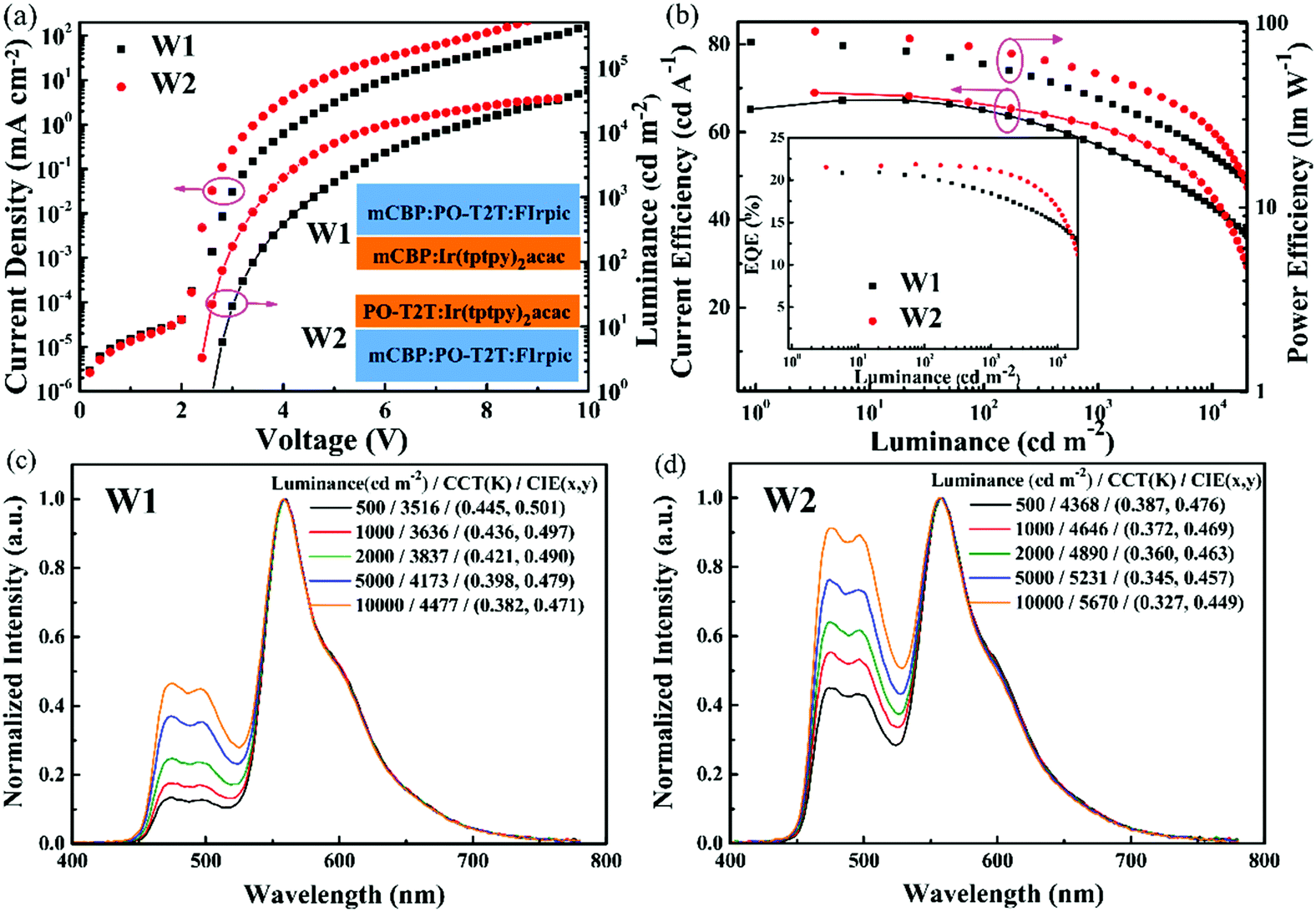
On the basis of the above strategies, we have prepared two WOLEDs with different EMLs of mCBP![[thin space (1/6-em)]](https://www.rsc.org/images/entities/char_2009.gif) :Ir(tptpy)2acac (4%, 6 nm)/mCBP:PO-T2T:FIrpic (1:1:10%, 12 nm) (W1) and mCBP:PO-T2T:FIrpic (1:1:10%, 12 nm)/PO-T2T:Ir(tptpy)2acac (4%, 6 nm) (W2). Although WOLEDs W1 and W2 have the same device structure except for the position and host of the orange phosphorescent emitter, the efficiency and roll-off of WOLEDs W1 and W2 exhibit a very large difference. As shown in Fig. 2a and Table 1, compared with W1 with a turn-on voltage (Von) of 2.8 V, a lower Von of 2.4 V and a larger current density are achieved in W2, which illustrates that the carrier injection, transport and recombination processes of W2 are more efficient than those of W1. From the current efficiency (CE), PE and EQE versus luminance characteristics, as shown in Fig. 2b, W2 exhibits a forward-viewing maximum CE, PE and EQE of 68.6 cd A−1, 90.2 lm W−1 and 21.9%, respectively, which are superior to 67.3 cd A−1, 75.4 lm W−1 and 20.9%, as displayed by W1. More importantly, the PEs and EQEs still retain 57.9 lm W−1 and 21.5% at 500 cd m−2, 51.2 lm W−1 and 21.1% at 1000 cd m−2, showing a very low efficiency roll-off of 3.7% in W2, which is also better than that of W1. This proves that the arrangement of the EML sequence plays a significant role in improving the performance of the fabricated WOLEDs.
:Ir(tptpy)2acac (4%, 6 nm)/mCBP:PO-T2T:FIrpic (1:1:10%, 12 nm) (W1) and mCBP:PO-T2T:FIrpic (1:1:10%, 12 nm)/PO-T2T:Ir(tptpy)2acac (4%, 6 nm) (W2). Although WOLEDs W1 and W2 have the same device structure except for the position and host of the orange phosphorescent emitter, the efficiency and roll-off of WOLEDs W1 and W2 exhibit a very large difference. As shown in Fig. 2a and Table 1, compared with W1 with a turn-on voltage (Von) of 2.8 V, a lower Von of 2.4 V and a larger current density are achieved in W2, which illustrates that the carrier injection, transport and recombination processes of W2 are more efficient than those of W1. From the current efficiency (CE), PE and EQE versus luminance characteristics, as shown in Fig. 2b, W2 exhibits a forward-viewing maximum CE, PE and EQE of 68.6 cd A−1, 90.2 lm W−1 and 21.9%, respectively, which are superior to 67.3 cd A−1, 75.4 lm W−1 and 20.9%, as displayed by W1. More importantly, the PEs and EQEs still retain 57.9 lm W−1 and 21.5% at 500 cd m−2, 51.2 lm W−1 and 21.1% at 1000 cd m−2, showing a very low efficiency roll-off of 3.7% in W2, which is also better than that of W1. This proves that the arrangement of the EML sequence plays a significant role in improving the performance of the fabricated WOLEDs.
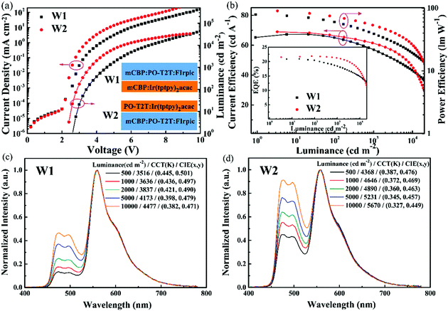 |
| | Fig. 2 (a) Current density and luminance versus driving voltage characteristics of W1 and W2. Inset: EML structures of W1 and W2. (b) Current efficiency and power efficiency versus luminance characteristics of W1 and W2. Inset: EQE versus luminance characteristics of W1 and W2. (c) EL spectra of W1 at different luminance values. (d) EL spectra of W2 at different luminance values. Device structure: ITO/HAT-CN (15 nm)/TAPC (60 nm)/TCTA (5 nm)/mCBP (5 nm)/EMLs/PO-T2T (45 nm)/Liq (1.5 nm)/Al (150 nm). The EMLs structure of W1 is mCBP:Ir(tptpy)2acac (4%, 6 nm)/mCBP:PO-T2T: FIrpic (1:1:10%, 12 nm). The EML structure of W2 is mCBP:PO-T2T:FIrpic (1:1:10%, 12 nm)/PO-T2T:Ir(tptpy)2acac (4%, 6 nm). | |
Table 1 Summary of key EL performance parameters for WOLEDs
| Device |
V
on
[V] |
PEmax/500/1000b [lm W−1] |
CEmax/500/1000b [cd A−1] |
EQEmax/500/1000b [%] |
Roll-off1000c (%) |
CCTc [K] |
CIE(x, y)c |
CRIc |
| Abbreviations: At a luminance of 1 cd m−2. The maximum efficiencies taken at 500 and 1000 cd m−2. Measured at 1000 cd m−2. |
| W1 |
2.7 |
75.4/44.7/38.9 |
67.3/59.7/57.0 |
20.9/19.1/18.4 |
12 |
3636 |
(0.436, 0.497) |
43 |
| W2 |
2.4 |
90.2/57.9/51/2 |
68.9/62.7/61.0 |
21.9/21.5/21.1 |
3.7 |
4646 |
(0.372, 0.469) |
52 |
| W3 |
2.4 |
87.6/52.2/48.8 |
67.5/61.5/59.1 |
20.8/20.1/19.5 |
6.3 |
4268 |
(0.396, 0.491) |
48 |
| W4 |
2.4 |
103.1/66.6/57.7 |
78.9/68.5/66.1 |
23.2/21.8/21.6 |
6.9 |
5082 |
(0.353, 0.488) |
48 |
The normalized EL spectra of devices W1 and W2 at different luminance values are shown Fig. 2c and d, respectively. Although they show varied spectra at different luminance values, they are yet good white emitters. The Commission International de I’Eclairage (CIE) coordinates of W1 and W2 are (0.436, 0.497) and (0.372, 0.469), respectively, at a luminance of 1000 cd m−2. Though the concentration and thickness of the orange EML are the same in W1 and W2, the light emission intensity of W2 in the blue spectral range is significantly higher than that of W1, which should be attributed to the difference in the exciton distribution region (EDR). As is known, the charge carrier mobility of electron-transporting materials generally increases more obviously than that of hole-transporting materials with increasing voltage, which would lead to a shift in the EDR. Thus, the main EDR in W1 should be located close to the interface between the blue EML and the orange EML, whereas the EDR in W2 should be close to the side of the pure mCBP layer, which will be analyzed in detail later.
Effect of dopants on charge carrier transport
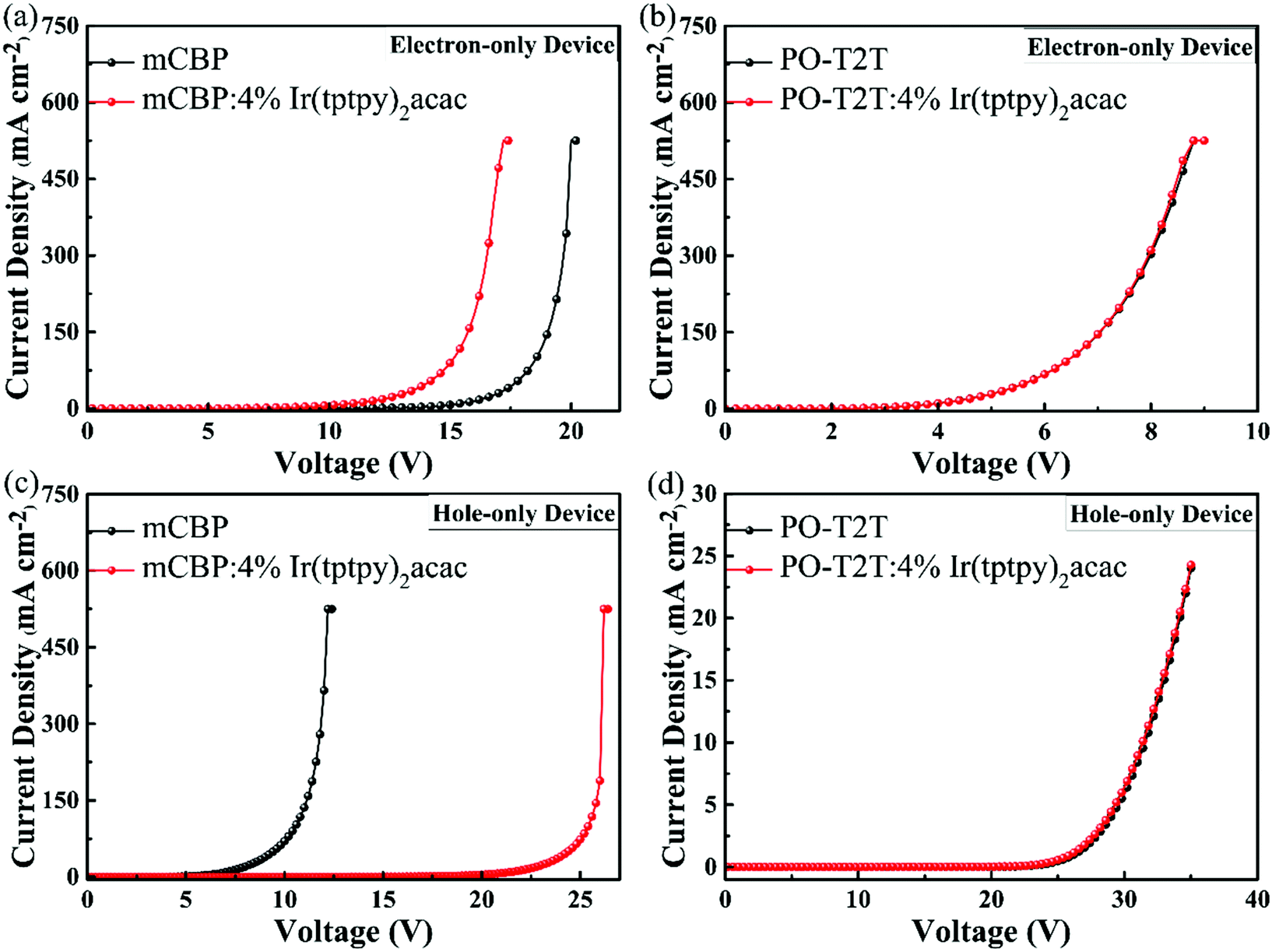
In order to reveal the great discrepancy in device performance between W1 and W2, a series of single carrier devices were tested to study the effects of phosphorescent dopants on charge carrier transport behavior. According to previous work, the blue emitter FIrpic doped in a mCBP:PO-T2T exciplex system served as a shallow trapping site for holes and played an assistant role in electron transport. Fig. 3a and b depict the current density versus voltage characteristics of the electron-only devices, based on mCBP and PO-T2T as the host of Ir(tptpy)2acac. It can be seen that the current density has a certain increase in the mCBP doped 4% Ir(tptpy)2acac case with respect to that of the pure mCBP, meaning that Ir(tptpy)2acac can facilitate electron transport. Comparatively, Ir(tptpy)2acac neither assists electron transport, nor has an electron trapping effect in the case of PO-T2T host. As we can see, compared to the electron-only device of the pure PO-T2T, the current density in PO-T2T doped 4% Ir(tptpy)2acac film does not change compared with that in pure PO-T2T film. Furthermore, in the case of the hole-only devices, as shown in Fig. 3c and d, the current density has a huge reduction when doping 4% Ir(tptpy)2acac into mCBP, illustrating that Ir(tptpy)2acac acted as a deep hole trapping site in mCBP. Similar to the electron-only device, Ir(tptpy)2acac doped in PO-T2T also does not change the hole current. Obviously, Ir(tptpy)2acac doped in PO-T2T does not affect the transport of electrons and holes. However, as we can see, the hole current in PO-T2T-based devices is far lower due to the poor hole mobility of PO-T2T. This should influence the location of exciton recombination in the white devices we fabricated. Moreover, from the relative energy levels of the orange dopant (HOMO = 5.1 eV, LUMO = 2.7 eV) and mCBP (HOMO = 6.1 eV, LUMO = 2.4 eV), where the orange dopant has a lower HOMO energy level and a higher LUMO energy level than the host (mCBP), could be beneficial for electron transporting and hole trapping, which is consistent with the above results. We also fabricated single carrier devices based on the white device structure, as shown in Fig. S2 (ESI†), and the experimental phenomenon also agrees with the above results. The strong hole-trapping effect of Ir(tptpy)2acac in mCBP affects the charge carrier balance and hole accumulation in the EML, resulting in low efficiency and serious efficiency roll-off, which could be the main reason for the poor EL performance of W1.
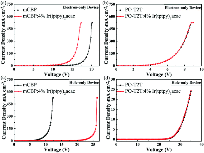 |
| | Fig. 3 Current density–voltage characteristics of single carrier devices. Electron-only devices of orange dopant co-doped in mCBP (a) and PO-T2T (b) host. Hole-only devices of orange dopant co-doped in mCBP (c) and PO-T2T (d) host. The hole-only device structure: ITO/HAT-CN (15 nm)/TAPC (60 nm)/TCTA (5 nm)/mCBP (5 nm)/pure host (10 nm) or host: guest (4%, 10 nm)/mCBP (5 nm)/TCTA (5 nm)/TAPC (60 nm)/HAT-CN (15 nm)/Al (150 nm). The electron-only device structure: ITO/Liq (1.5 nm)/PO-T2T (45 nm)/pure host (10 nm) or host: guest (4%, 10 nm)/PO-T2T (45 nm)/Liq (1.5 nm)/Al (150 nm). | |
Emission mechanism
To clarify the fundamental cause of the difference in EL performance between devices W1 and W2 in detail, we have further studied the emission mechanism of the orange dopant in these two devices. As is known, host–guest energy transfer and direct charge trapping on the guest are two emission mechanisms in doped OLEDs. As mentioned in previous work, there exist two emission processes for blue light emission in blue phosphor FIrpic doped exciplex devices: energy transfer from the exciplex to the FIrpic dopant and slightly direct charge trapping on FIrpic molecules.35 As indicated in Fig. 4a, the UV-vis absorption spectrum of Ir(tptpy)2acac in dichloromethane has a large overlap with the PL spectrum of mCBP:POT2T and mCBP:POT2T:FIrpic composite films, guaranteeing efficient energy transfer between them. As shown in Fig. 4b, the PL lifetime of blue emission located at 472 nm was partly quenched by the orange dopant from 1.50 μs to 0.85 μs when doping 4% Ir(tptpy)2acac into mCBP, which further proves that the energy transfer process to the orange dopant exists. Meanwhile, when doping 4% Ir(tptpy)2acac into PO-T2T, the PL lifetime of blue emission decreases to 0.7 μs, which is lower than that of mCBP, illustrating that the energy transfer process to Ir(tptpy)2acac in PO-T2T host is more effective than that in mCBP host. From the single carrier device data shown in Fig. 3, a substantial part of the orange emission in W1 also originates from the triplet excitons directly formed on Ir(tptpy)2acac molecules, whereas the energy transfer from the exciplex or FIrpic to Ir(tptpy)2acac molecules is the only way for orange emission in W2. Therefore, the reduction of charge carrier trapping on the dopant and the enhancement of energy transfer efficiency simultaneously become the key to the design of high performance WOLEDs.
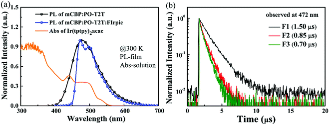 |
| | Fig. 4 (a) Normalized UV-vis absorption spectra of Ir(tptpy)2acac in dichloromethane, and PL spectra of mCBP:PO-T2T (1:1:10%, 30 nm) and mCBP:PO-T2T:FIrpic (1:1:10%, 30 nm, F1) mixed films. (b) PL decay curves of the films (F1, F2 and F3) measured at 472 nm with an excitation wavelength of 340 nm. The structure of film F1: mCBP:PO-T2T:FIrpic (1:1:10%, 30 nm). The structure of film F2: mCBP:PO-T2T:FIrpic (1:1:10%, 12 nm)/mCBP: Ir(tptpy)2acac (4%, 6 nm). The structure of film F3: mCBP:PO-T2T: FIrpic (1:1:10%, 12 nm)/PO-T2T: Ir(tptpy)2acac (4%, 6 nm). | |
Ultra-high efficiency WOLEDs
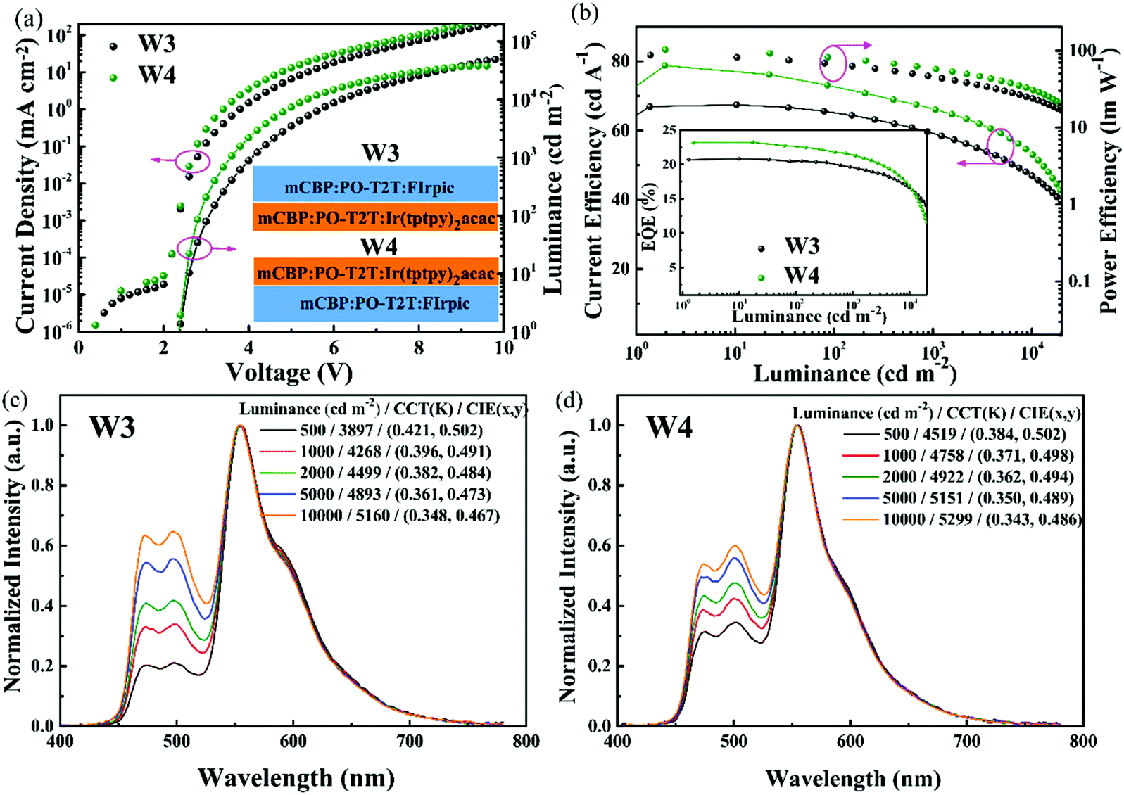
To elucidate the improved mechanism in efficiency and its roll-off in device B2, we first explored the exciton distribution profile in device B1 and B2. From the above analysis, the more efficient the energy transfer process from exciplex to orange phosphor, the higher the EL efficiency of the fabricated WOLED. In order to further improve the device performance, we doped the orange dopant into the mCBP:PO-T2T exciplex to decrease the energy transfer radius to further enhance the energy transfer efficiency. Before fabricating the WOLEDs, we studied the charge carrier transport properties of an Ir(tptpy)2acac doped mCBP:PO-T2T film. Fig. S3 (ESI†) shows the current density–voltage characteristics of the hole-only and electron-only devices. Clearly, the hole current is greatly decreased whereas the electron current does not change. This strongly indicates that Ir(tptpy)2acac molecules play a vital role in hole trapping. In order to extenuate the hole trapping effect, we have reduced the concentration of Ir(tptpy)2acac molecules in mCBP:PO-T2T and placed the doped orange EML between the blue EML and PO-T2T layers. As shown in Fig. 5 and Table 1, the optimal device W4 with EMLs of mCBP:PO-T2T:FIrpic (1:1:10%, 12 nm)/mCBP:PO-T2T:Ir(tptpy)2acac (1:1:1%, 6 nm) and the reference device W3 with EMLs of mCBP:PO-T2T:Ir(tptpy)2acac (1:1:1%, 6 nm)/mCBP:PO-T2T:FIrpic (1:1:10%, 12 nm) were fabricated. Compared to the reference device W3 with a maximum PE, CE and EQE of 87.6 lm W−1, 67.5 cd A−1 and 20.8%, respectively, W4 exhibits maximum forward-viewing efficiencies of 103.1 lm W−1, 78.9 cd A−1 and 23.2%, respectively, without using a light out-coupling technique, which have been significantly improved. Remarkably, the efficiencies still remain at 66.6 lm W−1, 68.5 cd A−1 and 21.8% at 500 cd m−2, and 57.7 lm W−1, 66.1 cd A−1 and 21.6% at 1000 cd m−2, respectively, also showing a low efficiency roll-off of 6.9%. This further proves the extreme significance of our strategies on designing high efficiency WOLEDs by accurately managing EML structures. Furthermore, the efficiencies of W4 are higher than those of WOLEDs with an EML of mCBP:PO-T2T:FIrpic:Ir(tptpy)2acac (1:1:10%:0.3% or 0.5%) whose maximum efficiencies are 93.6 lm W−1 and 22.8%, 94.8 lm W−1 and 22.0%, respectively (Fig. S4, ESI†). From the EL spectra of W3 and W4 at different luminance values from 500 cd m−2 to 10000 cd m−2 shown in Fig. 5c and d, the CIE coordinates and Correlated Color Temperature (CCT) of W3 and W4 are (0.396, 0.491) and (0.371, 0.498), and 4268 and 4758 K at 1000 cd m−2, respectively. The Color Rendering Index (CRI) is under 60 due to the lack of red light in the spectra.
 |
| | Fig. 5 (a) Normalized UV-vis absorption spectra of Ir(tptpy)2acac in dichloromethane, and PL spectra of mCBP:PO-T2T (1:1:10%, 30 nm) and mCBP:PO-T2T:FIrpic (1:1:10%, 30 nm, F1) mixed films. (b) PL decay curves of the films (F1, F2 and F3) measured at 472 nm with an excitation wavelength of 340 nm. The structure of film F1: mCBP:PO-T2T: FIrpic (1:1:10%, 30 nm). The structure of film F2: mCBP:PO-T2T:FIrpic (1:1:10%, 12 nm)/mCBP: Ir(tptpy)2acac (4%, 6 nm). The structure of film F3: mCBP:PO-T2T:FIrpic (1:1:10%, 12 nm)/PO-T2T: Ir(tptpy)2acac (4%, 6 nm). | |
Compared to W1 with the orange EML of mCBP: Ir(tptpy)2acac (4%, 6 nm) and W2 with the orange EML of PO-T2T: Ir(tptpy)2acac (4%, 6 nm), W3 and W4 with low doping concentration of orange dopant (1%) into the mCBP:PO-T2T exciplex host achieves higher EL performance. The improvement should be attributed to the more effective energy transfer from the mCBP:PO-T2T exciplex to the orange dopant. As shown in Fig. S5 (ESI†), the PL lifetimes of blue emission (observed at 478 and 472 nm) have a large reduction when doping Ir(tptpy)2acac into the mCBP:PO-T2T exciplex. Moreover, the Ir(tptpy)2acac peak shows a longer PL lifetime of 1.67 and 1.36 μs higher than its intrinsic PL decay time of 1.11 μs (Fig. S5c and d, ESI†), which also indicates that the energy transfer process is very effective. The reason that the efficiency of W4 is better than that of W3 can be attributed to the weaker hole-trapping effect in W4, which is confirmed by the single carrier devices shown in Fig. S6 (ESI†). Clearly, when the orange dopant is co-doped into the exciplex, the hole current of HD1-2 with the same EMLs as W3 decreases more seriously than that of HD2-2 with the same EMLs as W4, whereas the orange dopant has no obvious influence on the electron currents.
Concentration effects of phosphorescent dopants
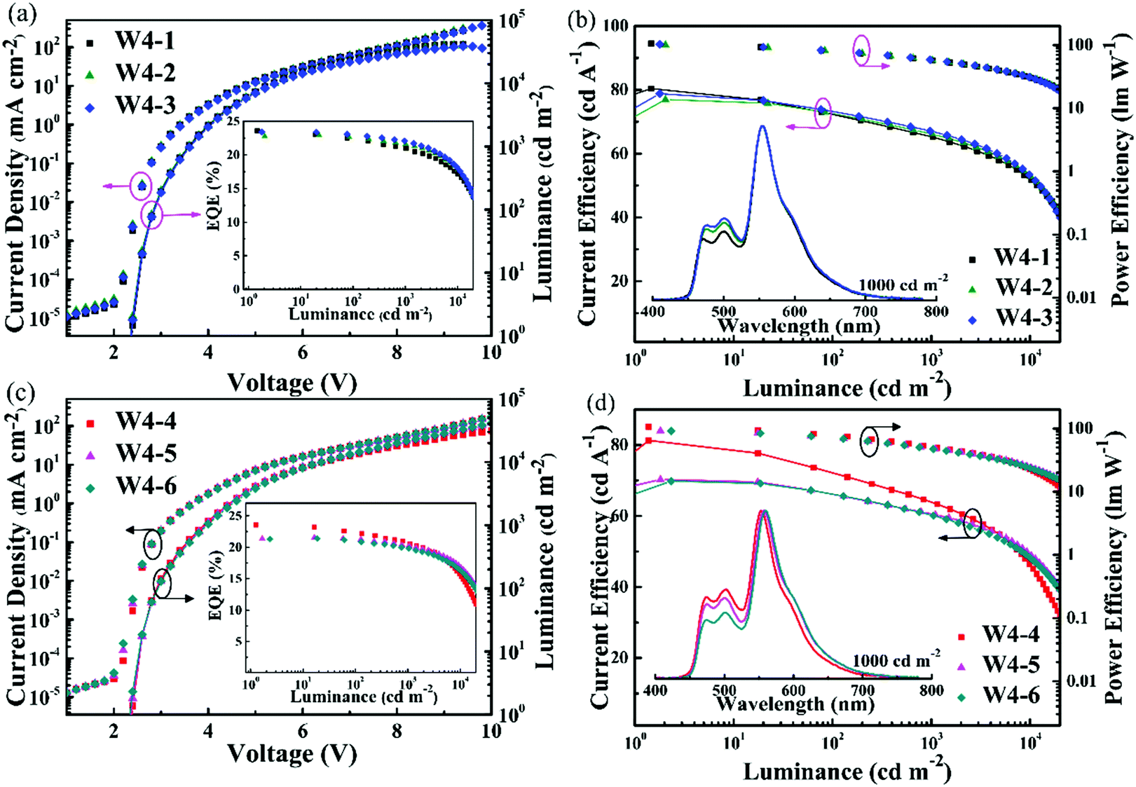
As mentioned above, the phosphorescent dopants in the host indeed have important effects on the charge carrier behavior. Therefore, the change in doping concentration in the host will affect the charge carrier injection, transport, and recombination process, further affecting device EL performance. To evaluate the influence of phosphorescent dopants, we examined the concentration dependent properties based on device W4. As shown in Fig. 6a, b, Fig. S7, Table 2, and Table S1 (ESI†), as the concentration of FIrpic increases, the J–V characteristics of these devices have a slight change, but the efficiencies and roll-off have been obviously improved, particularly at high luminance. When the concentration becomes greater than 2%, the maximum PEs, CEs and EQEs have exceeded 100 lm W−1, 77 cd A−1 and 23%, respectively. The EQEs are still over 21% at a luminance of 1000 cd m−2, exhibiting low efficiency roll-off. Clearly, the doping of FIrpic has a tiny effect on charge carrier transport, and the singlet and triplet excitons can be efficiently transferred from the exciplex host to FIrpic without energy loss due to the low energy gap between the T1 of exciplex (2.63 eV) and that of FIrpic (2.62 eV), which is the reason why the devices have such high performance. However, as shown in Fig. 6c, d and Table 2, with increasing the dopant concentration of Ir(tptpy)2acac molecules, the blue emission is gradually reduced, indicating that more excitons are used by Ir(tptpy)2acac for orange emission. The efficiencies are also decreased due to the serious hole-trapping effect and exciton aggregation in the orange EML. The most remarkable forward-viewing efficiencies of PE as high as 106.4 lm W−1, CE as high as 81.3 cd A−1 and EQE as high as 23.5% were achieved by optimizing the orange dopant concentration of 0.5%.
 |
| | Fig. 6 (a) Current density and luminance versus driving voltage characteristics of WOLEDs (W4-1, W4-2, W4-3) with different concentrations of FIrpic. Inset: EQE versus luminance characteristics of W4-1, W4-2 and W4-3. (b) Current efficiency and power efficiency versus luminance characteristics of W4-1, W4-2 and W4-3. Inset: EL spectra of WOLEDs at a luminance of 1000 cd m−2. (c) Current density and luminance versus driving voltage characteristics of WOLEDs (W4-4, W4-5, W4-6) with different concentrations of Ir(tptpy)2acac. Inset: EQE versus luminance characteristics of W4-4, W4-5 and W4-6. (d) Current efficiency and power efficiency versus luminance characteristics of W4-4, W4-5 and W4-6. Inset: EL spectra of WOLEDs at a luminance of 1000 cd m−2. Device structure: ITO/HAT-CN (15 nm)/TAPC (60 nm)/TCTA (5 nm)/mCBP (5 nm)/mCBP:PO-T2T:FIrpic (1:1:X, 12 nm)/mCBP:PO-T2T:Ir(tptpy)2acac (1:1:Y, 6 nm)/PO-T2T (45 nm)/Liq (1.5 nm)/Al (150 nm). W4-1: X = 5%, Y = 1%; W4-2: X = 15%, Y = 1%; W4-3: X = 20%, Y = 1%; W4-4: X = 10%, Y = 0.5%; W4-5: X = 10%, Y = 3%; W4-6: X = 10%, Y = 6%. | |
Table 2 Summary of key EL parameters for white devices
| Device |
V
on
[V] |
PEmax/500/1000b [lm W−1] |
CEmax/500/1000b [cd A−1] |
EQEmax/500/1000b [%] |
Roll-off1000c (%) |
CCTc [K] |
CIE(x, y)c |
CRIc |
| Abbreviations: At a luminance of 1 cd m−2. The maximum efficiencies and values taken at 500 and 1000 cd m−2. Measured at 1000 cd m−2. |
| W4-1 |
2.4 |
105.2/64.3/56.9 |
80.4/67.7/65.2 |
23.6/21.5/21.0 |
11 |
4696 |
(0.373,0.495) |
45 |
| W4-2 |
2.4 |
100.7/65.1/57.7 |
77.0/68.3/66.1 |
23.0/21.9/21.6 |
6.1 |
4762 |
(0.370,0.495) |
46 |
| W4-3 |
2.4 |
103.1/66.5/58.6 |
78.8/69.2/67.1 |
23.4/22.4/22.0 |
6 |
4808 |
(0.367,0.493) |
46 |
| W4-4 |
2.4 |
106.4/61.2/51.1 |
81.3/66.8/64.1 |
23.5/21.3/20.5 |
12.8 |
5212 |
(0.347,0.497) |
45 |
| W4-5 |
2.4 |
91.9/57.5/48.3 |
70.3/62.5/60.8 |
21.5/20.8/20.3 |
5.6 |
4651 |
(0.375,0.485) |
48 |
| W4-6 |
2.4 |
91.4/56.9/47.2 |
69.8/62.2/60.1 |
21.4/20.3/19.8 |
7.5 |
4353 |
(0.391,0.491) |
46 |
For comparison with device W4, three groups of devices based on the EML structures of W1, W2 and W3 were fabricated by changing the doping concentration of Ir(tptpy)2acac and fixing the FIrpic concentration at 10% in the mCBP:PO-T2T exciplex host. It can be seen from Fig. S8–S10 and Tables S2–S4 (ESI†) that when the doping concentration is very low, more excitons are transferred from the exciplex to FIrpic for blue emission, resulting in cold white emission with high CCT. With the concentration increasing, the relative intensity of the EL spectra in the orange emission range was gradually enhanced, implying more efficient energy transfer to Ir(tptpy)2acac molecules. And the efficiencies and the roll-off in devices based on the EML structures of W1 and W3 decrease more clearly than those of W2 and W4, which further illustrates that decreasing the hole-trapping effect and increasing the energy transfer efficiency are helpful for improving device performance.
Three-color WOLEDs
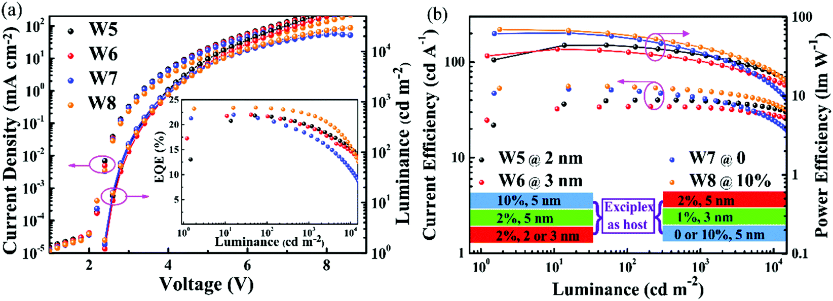
Based on the above exploration, ultra-high efficiency and low efficiency roll-off complementary color WOLEDs have been realized through a valid arrangement of EMLs. However, the CRI of two-color WOLEDs is low, which restrains their commercial application in SSL. WOLEDs should be broad and continuous covering the entire visible-light spectral region for higher CRI.36–38 Thus, three-color WOLEDs using green dopant Ir(ppy)2acac and red dopant RD071 to replace the orange dopant Ir(tptpy)2acac were fabricated. In order to design appropriate EML structures, we have investigated the effects of green/red dopant on the charge carrier transport behavior. As shown in the J–V characteristics of single-carrier devices (see Fig. S11, ESI†), as doping Ir(ppy)2acac and RD071 into the mCBP:PO-T2T exciplex host, the electron currents remain nearly unchanged, while the hole currents remarkably decrease, indicating that electron transport is affected slightly by doped Ir(ppy)2acac and RD071, but they play a role in strong hole trapping. Based on this, WOLEDs with red-green-blue and blue-green-red sequence EMLs were fabricated (see Fig. 7 and Table S5, ESI†). All of the three-color devices realize a low Von of 2.4 V due to the barrier-free injection to the EMLs. The blue-green-red devices W7 and W8 with FIrpic concentrations of 0 and 10% achieve maximum forward-viewing efficiencies of 63.0 lm W−1, 52.2 cd A−1 and 22.0%, 69.6 lm W−1, 55.9 cd A−1 and 23.4%, for PE, CE and EQE, respectively, which are superior to 44.3 lm W−1, 40.2 cd A−1 and 21.8%, 39.2 lm W−1, 34.3 cd A−1 and 22.0% in the red-green-blue devices W5 and W6 with different thicknesses of red EML (2 nm for W5, 3 nm for W6). Furthermore, the EQE still retains 22.1% at 1000 cd m−2, exhibiting a low efficiency roll-off of 5.6% in W8 with 10% FIrpic. This also illustrates that accurately regulating the dopant concentration and the arrangement of the EMLs is very important for high performance WOLEDs. Fig. S12 (ESI†) shows the normalized EL spectra at different luminance levels. The CIE coordinates, CCTs and CRIs are (0.512, 0.445), 2336 K and 81, (0.554, 0.410), 1777 K and 77, (0.432, 0.489), 3654 K and 80, and (0.361, 0.460), 4859 K and 78, respectively, for devices W5-8 at 1000 cd m−2. The color-shift in the EL spectra may be attributed to the change in exciton distribution region with different voltages. To fully improve the stability of the EL spectra, based on our design strategy, the separation of the exciton emission zone from the exciton recombination zone would be helpful, which is under investigation in our group.
 |
| | Fig. 7 (a) Current density and luminance versus driving voltage characteristics of three-color WOLEDs (W5-8) with different EMLs. Inset: EQE versus luminance characteristics of W5-8. (b) Current efficiency and power efficiency versus luminance characteristics of W5-8. Inset: EMLs structure diagram of WOLEDs. | |
Conclusions
In summary, a series of ultra-high efficiency WOLEDs based on an exciplex as host with multi-EMLs have been successfully demonstrated by optimizing the doped phosphor concentration and the sequence of different color layers. It can be clearly seen that the careful manipulation of dopant concentration and rational arrangement of the emitters are beneficial to enhancing the energy transfer efficiency and reducing the carrier trapping effect, thus improving efficiency and efficiency roll-off. By optimizing, maximum EQEs exceeding 23% are achieved in the fabricated WOLEDs, and still retain over 22% at 1000 cd m−2, showing a tiny efficiency roll-off. We believe that this design concept in the exciplex forming co-host system provides a reliable avenue for the future development of high efficiency and low efficiency roll-off WOLEDs.
Conflicts of interest
There are no conflicts to declare.
Acknowledgements
The authors gratefully acknowledge the National Key Research and Development Plan of China (2016YFB0400701), the National Natural Science Foundation of China (21788102, 51333007, 91433201, 11661131001), Guangzhou Science & Technology Plan Project (201707020040) and the Foundation of Guangzhou Science and Technology Project (201504010012) for the support of this research.
Notes and references
- S. Reineke, F. Lindner, G. Schwartz, N. Seidler, K. Walzer, B. Luessem and K. Leo, Nature, 2009, 459, 234 CrossRef CAS PubMed.
- G. Zhou, W. Y. Wong and S. Suo, J. Photochem. Photobiol., C, 2010, 11, 133 CrossRef CAS.
- H. Sasabe and J. Kido, Eur. J. Org. Chem., 2013, 7653 CrossRef CAS.
- H. H. Kuo, Z. L. Zhu, C. S. Lee, Y. K. Chen, S. H. Liu, P. T. Chou, A. K. Jen and Y. Chi, Adv. Sci., 2018, 5, 1800846 CrossRef PubMed.
- X. Yang, H. Guo, B. Liu, J. Zhao, G. Zhou, Z. Wu and W. Y. Wong, Adv. Sci., 2018, 5, 1701067 CrossRef PubMed.
- J. Wang, J. Chen, X. Qiao, S. M. Alshehri, T. Ahamad and D. Ma, ACS Appl. Mater. Interfaces, 2016, 8, 10093 CrossRef CAS PubMed.
- S. F. Wu, S. H. Li, Y. K. Wang, C. C. Huang, Q. Sun, J. J. Liang, L. S. Liao and M. K. Fung, Adv. Funct. Mater., 2017, 27, 1701314 CrossRef.
- D. Zhang, M. Cai, Y. Zhang, D. Zhang and L. Duan, ACS Appl. Mater. Interfaces, 2015, 7, 28693 CrossRef CAS PubMed.
- S. J. Su, E. Gonmori, H. Sasabe and J. Kido, Adv. Mater., 2008, 24, 4189 Search PubMed.
- M. Du, Y. Feng, D. Zhu, T. Peng, Y. Liu, Y. Wang and M. R. Bryce, Adv. Mater., 2016, 28, 5963 CrossRef CAS PubMed.
- Y. L. Chang, Y. Song, Z. Wang, M. G. Helander, J. Qiu, L. Chai, Z. Liu, G. D. Scholes and Z. Lu, Adv. Funct. Mater., 2013, 23, 705 CrossRef CAS.
- X. Tang, X. Y. Liu, Y. Yuan, Y. J. Wang, H. C. Li, Z. Q. Jiang and L. S. Liao, ACS Appl. Mater. Interfaces, 2018, 10, 29840 CrossRef CAS PubMed.
- J. Lee, H. F. Chen, T. Batagoda, C. Coburn, P. I. Djurovich, M. E. Thompson and S. R. Forrest, Nat. Mater., 2016, 15, 92 CrossRef CAS PubMed.
- Y. R. Sun, N. C. Giebink, H. Kanno, B. W. Ma, M. E. Thompson and S. R. Forrest, Nature, 2006, 440, 908 CrossRef CAS PubMed.
- Y. Tao, C. Yang and J. Qin, Chem. Soc. Rev., 2011, 40, 2943 RSC.
- C. W. Lee and J. Y. Lee, Adv. Mater., 2013, 25, 5450 CrossRef CAS PubMed.
- H. Shin, S. Lee, K. H. Kim, C. K. Moon, S. J. Yoo, J. H. Lee and J. J. Kim, Adv. Mater., 2014, 26, 4730 CrossRef CAS PubMed.
- Z. Liu, M. G. Helander, Z. Wang and Z. Lu, Org. Electron., 2013, 14, 852 CrossRef CAS.
- Z. W. Liu, M. G. Helander, Z. B. Wang and Z. Lu, Appl. Phys. Lett., 2009, 94, 113305 CrossRef.
- C. Yun, J. Lee, J. Lee, B. Lüssem, F. Ventsch, K. Leo and M. C. Gather, Appl. Phys. Lett., 2012, 101, 243303 CrossRef.
- J. Lee, C. Jeong, T. Batagoda, C. Coburn, M. E. Thompson and S. R. Forrest, Nat. Commun., 2017, 8, 15566 CrossRef CAS PubMed.
- Y. Zhang, J. Lee and S. R. Forrest, Nat. Commun., 2014, 5, 5008 CrossRef CAS PubMed.
- L. Zhu, Y. Zhao, H. Zhang, J. Chen and D. Ma, J. Appl. Phys., 2014, 115, 244511 CrossRef.
- Q. Wang, J. Ding, D. Ma, Y. Cheng, L. Wang, X. Jing and F. Wang, Adv. Funct. Mater., 2009, 19, 84 CrossRef CAS.
- M. Sarma and K. T. Wong, ACS Appl. Mater. Interfaces, 2018, 10, 19279 CrossRef CAS PubMed.
- J. H. Lee, S. Lee, S. J. Yoo, K. H. Kim and J. J. Kim, Adv. Funct. Mater., 2014, 24, 4681 CrossRef CAS.
- K. H. Kim, S. Lee, C. K. Moon, S. Y. Kim, Y. S. Park, J. H. Lee, J. Woo Lee, J. Huh, Y. You and J. J. Kim, Nat. Commun., 2014, 5, 4769 CrossRef CAS PubMed.
- X. K. Liu, Z. Chen, J. Qing, W. J. Zhang, B. Wu, H. L. Tam, F. Zhu, X. H. Zhang and C. S. Lee, Adv. Mater., 2015, 27, 7079 CrossRef CAS PubMed.
- D. Feng, D. Dong, L. Lian, H. Wang and G. He, Org. Electron., 2018, 56, 216 CrossRef CAS.
- J. H. Lee, H. Shin, J. M. Kim, K. H. Kim and J. J. Kim, ACS Appl. Mater. Interfaces, 2017, 9, 3277 CrossRef CAS PubMed.
- C. J. Shih, C. C. Lee, Y. H. Chen, S. Biring, G. Kumar, T. H. Yeh, S. Sen, S. W. Liu and K. T. Wong, ACS Appl. Mater. Interfaces, 2018, 10, 2151 CrossRef CAS PubMed.
- H. Shin, J. H. Lee, C. K. Moon, J. S. Huh, B. Sim and J. J. Kim, Adv. Mater., 2016, 28, 4920 CrossRef CAS PubMed.
- Y. S. Park, S. Lee, K. H. Kim, S. Y. Kim, J. H. Lee and J. J. Kim, Adv. Funct. Mater., 2013, 23, 4914 CrossRef CAS.
- X. Du, J. Zhao, S. Yuan, C. Zheng, H. Lin, S. Tao and C. S. Lee, J. Mater. Chem. C, 2016, 4, 5907 RSC.
- S. Ying, D. Yang, X. Qiao, Y. Dai, Q. Sun, J. Chen, T. Ahamad, S. M. Alshehri and D. Ma, J. Mater. Chem. C, 2018, 6, 10793 RSC.
- S. Wu, S. Li, Q. Sun, C. Huang and M. K. Fung, Sci. Rep., 2016, 6, 25821 CrossRef CAS PubMed.
- Y. Miao, K. Wang, B. Zhao, L. Gao, Y. Wang, H. Wang, B. Xu and F. Zhu, J. Mater. Chem. C, 2017, 5, 12474 RSC.
- Y. Miao, K. Wang, B. Zhao, L. Gao, P. Tao, X. Liu, Y. Hao, H. Wang, B. Xu and F. Zhu, Nanophotonics, 2018, 7, 295 CAS.
Footnote |
| † Electronic supplementary information (ESI) available. See DOI: 10.1039/c9qm00017h |
|
| This journal is © the Partner Organisations 2019 |
Click here to see how this site uses Cookies. View our privacy policy here. 
 ,
Qian
Sun
,
Qian
Sun