
Highly-efficient semi-transparent organic solar cells utilising non-fullerene acceptors with optimised multilayer MoO3/Ag/MoO3 electrodes†
Guangjun
Sun
a,
Munazza
Shahid
a,
Zhuping
Fei
 b,
Shenda
Xu
c,
Flurin D.
Eisner
d,
Thomas D.
Anthopolous
e,
Martyn A.
McLachlan
b and
Martin
Heeney
*a
b,
Shenda
Xu
c,
Flurin D.
Eisner
d,
Thomas D.
Anthopolous
e,
Martyn A.
McLachlan
b and
Martin
Heeney
*a
aDepartment of Chemistry and Centre for Plastic Electronics, Imperial College London, SW7 2AZ, UK. E-mail: m.heeney@imperial.ac.uk
bInstitute of Molecular Plus, Tianjin Key Laboratory of Molecular Optoelectronic Science, Tianjin University, Tianjin, 300072, P. R. China
cDepartment of Materials and Centre for Plastic Electronics, Imperial College London, London SW7 2AZ, UK
dDepartment of Physic and Centre for Plastic Electronics, Imperial College London, London SW7 2AZ, UK
eDivision of Physical Sciences and Engineering, King Abdullah University of Science and Technology, Saudi Arabia
First published on 18th January 2019
Abstract
We report the optimisation of a semi-transparent solar cell based on a blend of a recently reported high performance donor polymer (PFBDB-T) with a non-fullerene acceptor derivative (C8-ITIC). The performance is shown to strongly depend on the nature of the semi-transparent electrode, and we report the optimal fabrication conditions for a multilayer MoO3/Ag/MoO3 electrode. The effect of deposition rate and layer thickness of both the Ag and the outer MoO3 on transparency and sheet resistance is investigated, and is shown to have a significant impact on the overall device performance. The optimised PFBDB-T:C8-ITIC based devices exhibit an average power conversion efficiency (PCE) of 9.2% with an average visible transmittance (AVT) of 22%.
Introduction
Organic solar cells (OSCs) have been recognised as one of the most promising thin film photovoltaic technologies, offering the potential to fabricate lightweight devices by a variety of low-cost deposition techniques. The ability to readily tune the absorption spectrum of the organic semiconducting components via structural modifications offers an attractive route to semi-transparent organic solar cell (ST-OSC) applications. For example, the colour of the cell can, in principle, be readily tuned for aesthetic reasons in power-generating windows or to avoid overlap with the absorption of chlorophyll in photovoltaic greenhouses.1–3 The recent development of high performance alternatives to fullerenes as the electron accepting component of the blend has stimulated more interest in ST-OSC applications.4 The band gap of such non-fullerene acceptors (NFAs) can be more readily tuned than with fullerene derivatives, allowing the development of cells which generate significant photocurrent from the infrared region of the solar spectrum.5–7In addition to tuning the band gap of the active layer, the performance of a ST-OSC is also highly dependent on the nature of the transparent electrodes utilised. Indium doped tin oxide (ITO) is one of the most common electrodes used for ST-OSCs. Typically, the work function of ITO is such that it is used as the hole-extracting (HE) electrode. However for most ST-OPV devices, the so-called inverted device architecture is used,8 in which the glass/ITO substrate is coated with a thin interlayer to modify the work function such that it behaves as the electron-extracting (EE) electrode. Typical treatments include semiconducting metal oxides such as ZnO or TiO2. In the case of inverted ST devices, the transparent HE electrode must then be deposited on top of the active semiconducting layer without causing any damage to the underlying layer. Some candidate materials for the transparent HE electrode include Ag nanowires,9 ultra-thin high work function metal electrodes10,11 and dielectric/metal/dielectric (DMD) sandwich electrodes.12,13
Nanowire based electrodes show much promise9,14,15 but issues such as large junction resistance between nanowires, high surface roughness and random nanowire alignment can hinder the performance. Ultrathin metal electrodes are a potentially attractive solution since the average visible transmittance (AVT) of the device can be readily increased by reducing the metal thickness. For example, reducing Ag thickness from 60 nm to 6 nm is reported to increase AVT from 2% to near 36%.10 However, very thin layers typically have a high sheet resistance and consequently lower OSC performance. In addition, the Ag side can give a stronger reflectance than the ITO side, causing an undesirable optical asymmetry of ST-OSC devices.6,11 The use of multilayer electrodes, especially so-called dielectric/metal/dielectric (DMD) has been one approach to reduce the reflectivity and improve the optical characteristics. In particular multilayer MoO3/Ag/MoO3 electrodes, where the addition of the outer MoO3 significantly reduced the reflectance of the Ag film, have shown promise.12,13,16 Multilayer electrodes have been reported with improved conductivity compared with ITO, albeit with slightly lower transmittance.17 ST-OSC devices based on the non-fullerene acceptor ITIC18 (3,9-bis(2-methylene-(3-(1,1-dicyanomethylene)-indanone))-5,5,11,11-tetrakis(4-hexylphenyl)-dithieno[2,3-d:2′,3′-d′]-s-indaceno-[1,2-b:5,6-b′]dithiophene) using MoO3/Ag/MoO3 electrodes exhibited a PCE up to 7.4% and average visible transmittance (AVT) of 25%.13
We have recently reported the synthesis of a new NFA, C8-ITIC {(2Z)-2-[(8-{(E)-[1-(dicyanomethylidene)-3-oxo-1,3-dihydro-2H-inden-2-ylidene]methyl}-6,6,12,12-tetraoctyl-6,12-dihydrothieno[3,2-b]thieno[2′′,3′′:4′,5′]thieno[2′,3′:5,6]-sindaceno[2,1-d]thiophen-2-yl)methylidene]-3-oxo-2,3-dihydro-1Hinden-1-ylidene}propanedinitrile (Scheme 1). This is an analogue of the previously reported ITIC, in which the phenylalkyl groups were replaced with linear alkyl side chains.19 This resulted in a small reduction in the optical band gap and an increase in crystallinity. When paired with a fluorinated donor polymer, PFBDB-T [poly[(2,6-(4,8-bis(5-(2-ethylhexyl)thiophen-2-yl)-benzo[1,2-b:4,5-b′]dithiophene))-alt-(5,5-(1′,3′-bis(4-fluorothiophen-2-yl))-5′,7′-bis(2-ethylhexyl)benzo[1′,2′-c:4′,5′-c′]dithiophene-4,8-dione)], devices with power conversion efficiencies (PCEs) of up to 13.2% have been achieved. The promising performance of the blend coupled with its strong absorption in the near-IR region (Fig. 1) led us to believe it was a good candidate for a ST-OSC. In this report we discuss the fabrication of optimised devices using this blend. In particular, we investigate the optimal deposition process for the multi-layer hole extracting electrodes.
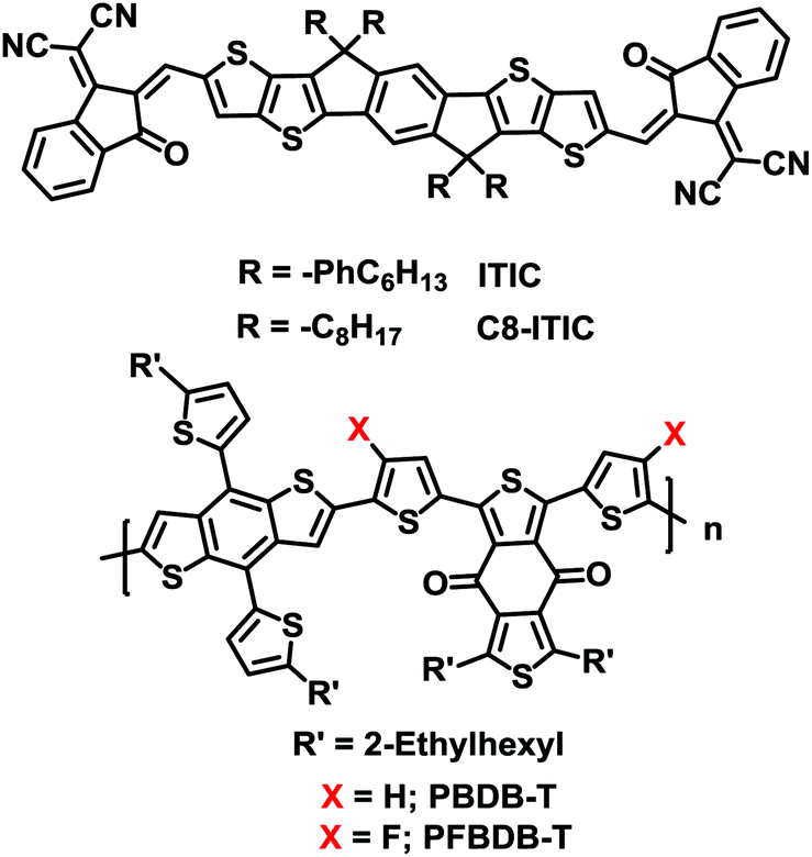 | ||
| Scheme 1 Chemical structures of ITIC, C8-ITIC, PBDB-T and PFBDB-T. | ||
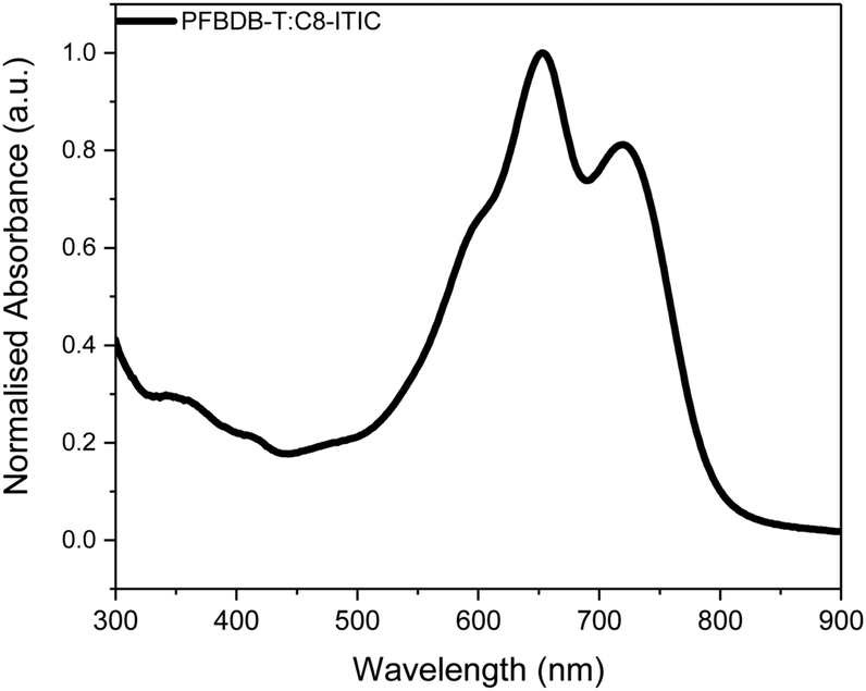 | ||
| Fig. 1 Absorption spectrum of PFBDB-T:C8-ITIC blend film. | ||
Experimental
Prior to fabrication, glass substrates were sequentially cleaned with detergent, acetone and isopropanol. The standard electrode (MoO3/Ag) was used to investigate the influence of Ag thickness and deposition rate on its performance. The multilayer MoO3/Ag/MoO3 electrodes were prepared to assess the influence of outer MoO3 thickness on the optical properties of our electrodes. The deposition was performed using thermal evaporator at a base pressure under 10−6 mbar. Deposition rates were measured with a quartz crystal microbalance, and the quoted layer thickness is based on the measured deposition rate. The deposition rate of MoO3 films was at a fixed value of 1.0 Å s−1, whilst the deposition rate of the Ag films ranged from 0.2 to 1.5 Å s−1. The first MoO3 layer was fixed at 10 nm thickness while the MoO3 deposited on the Ag layer ranged in thickness from 0 to 40 nm. The after evaporation, the sheet resistance (Rsheet) of each electrode was measured using a four-point probe setup (Jandel RM3000 Test Unit) and the transmittance and reflectance spectra of both types of electrode were measured using a UV-2600 Shimadzu UV-Vis spectrometer. Scanning electron microscopy (SEM) was used to interrogate the topography of Ag films using a LEO 1525 Gemini high-resolution field emission gun scanning electron microscope.Devices were fabricated onto ITO coated glass substrates that, prior to use, were sequentially cleaned with detergent, acetone and isopropanol with the aid of ultrasonics and subsequently dried under a N2 stream. Immediately prior to spin casting, the substrates were further subjected to cleaning by UV-Ozone. A ZnO nanoparticle solution (1.25 wt% ZnO in isopropanol) was spin-coated on top of ITO at 4000 rpm for 40 s, then annealed at 110 °C for 10 min. The devices were transferred to a nitrogen-purged glove box to complete the active layer deposition. A solution of PFBFB-T![[thin space (1/6-em)]](https://www.rsc.org/images/entities/char_2009.gif) :C8-ITIC (1:1.25 weight ratio) was dissolved in chlorobenzene (20 mg mL−1) at stirred overnight at 50 °C overnight. The blend solution was deposited by spin-coating at 2000 rpm for 60 seconds. Finally, MoO3 and Ag were evaporated through a shadow mask to define devices with an area of 0.045 cm2. The current density–voltage (J–V) characteristics of the OSCs were measured with a Keithley 2400 Source-Measure Unit under air mass (AM) 1.5 illumination at a calibrated light intensity of 100 mW cm−2. All measurements were performed within a N2-purged chamber with the device illuminated from the bottom (glass/ITO) layer. The external quantum efficiencies (EQEs) of the devices were obtained using the PVE300 photovoltaic quantum efficiency system with incident light calibrated to AM 1.5 solar spectrum.
:C8-ITIC (1:1.25 weight ratio) was dissolved in chlorobenzene (20 mg mL−1) at stirred overnight at 50 °C overnight. The blend solution was deposited by spin-coating at 2000 rpm for 60 seconds. Finally, MoO3 and Ag were evaporated through a shadow mask to define devices with an area of 0.045 cm2. The current density–voltage (J–V) characteristics of the OSCs were measured with a Keithley 2400 Source-Measure Unit under air mass (AM) 1.5 illumination at a calibrated light intensity of 100 mW cm−2. All measurements were performed within a N2-purged chamber with the device illuminated from the bottom (glass/ITO) layer. The external quantum efficiencies (EQEs) of the devices were obtained using the PVE300 photovoltaic quantum efficiency system with incident light calibrated to AM 1.5 solar spectrum.
Results and discussion
Typically, there are two approaches towards improving the transmittance of ST-OSCs, either reducing the thickness of the active layer, although this clearly reduces the amount of photocurrent that can be produced, or by optimising the transparent electrode. In this work, we have investigated the latter, using either bilayer MoO3/Ag or trilayer MoO3/Ag/MoO3 electrodes (Fig. 2).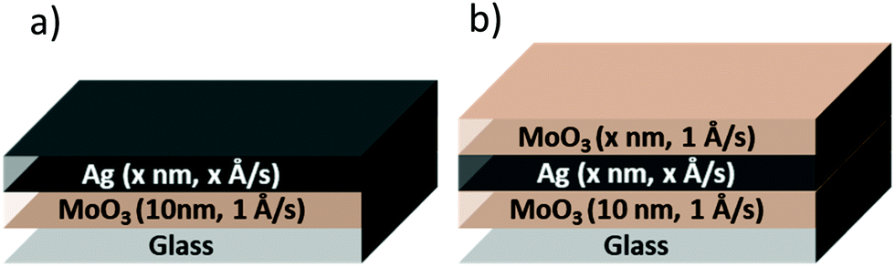 | ||
| Fig. 2 Schematic diagram of the electrode structures: (a) normal MoO3/Ag; (b) multilayer MoO3/Ag/MoO3. | ||
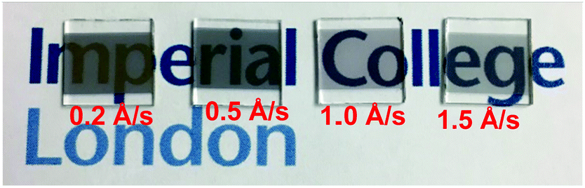
Our initial studies focussed on the optimisation of the deposition rate and thickness of the Ag in a bilayer architecture, using a fixed thickness of MoO3 (10 nm). Initially, deposition rates of 0.2, 0.5, 1.0 and 1.5 Å s−1 were used to deposit 10 nm of Ag. The transmittance spectra of the electrodes are presented in Fig. 3a and their visual appearance is shown in Table 1. The AVT was calculated from the arithmetic mean of the transmittance spectra within the range of 390–700 nm. The results are shown in Table 1 together with the measured sheet resistance (Rsheet). The results clearly show that an increase in the deposition rate results in an improvement of transmittance over the entire visible region (390–700 nm), as well as a reduction in sheet resistance. Since faster deposition rates afforded more promising results, we used the faster two rates i.e. 1.0 and 1.5 Å s−1 to investigate the influence of Ag thickness (Fig. 3b). The results show that the AVT decreases steadily as Ag film thickness increases, and that thicker films afford better conductivity (see ESI†).
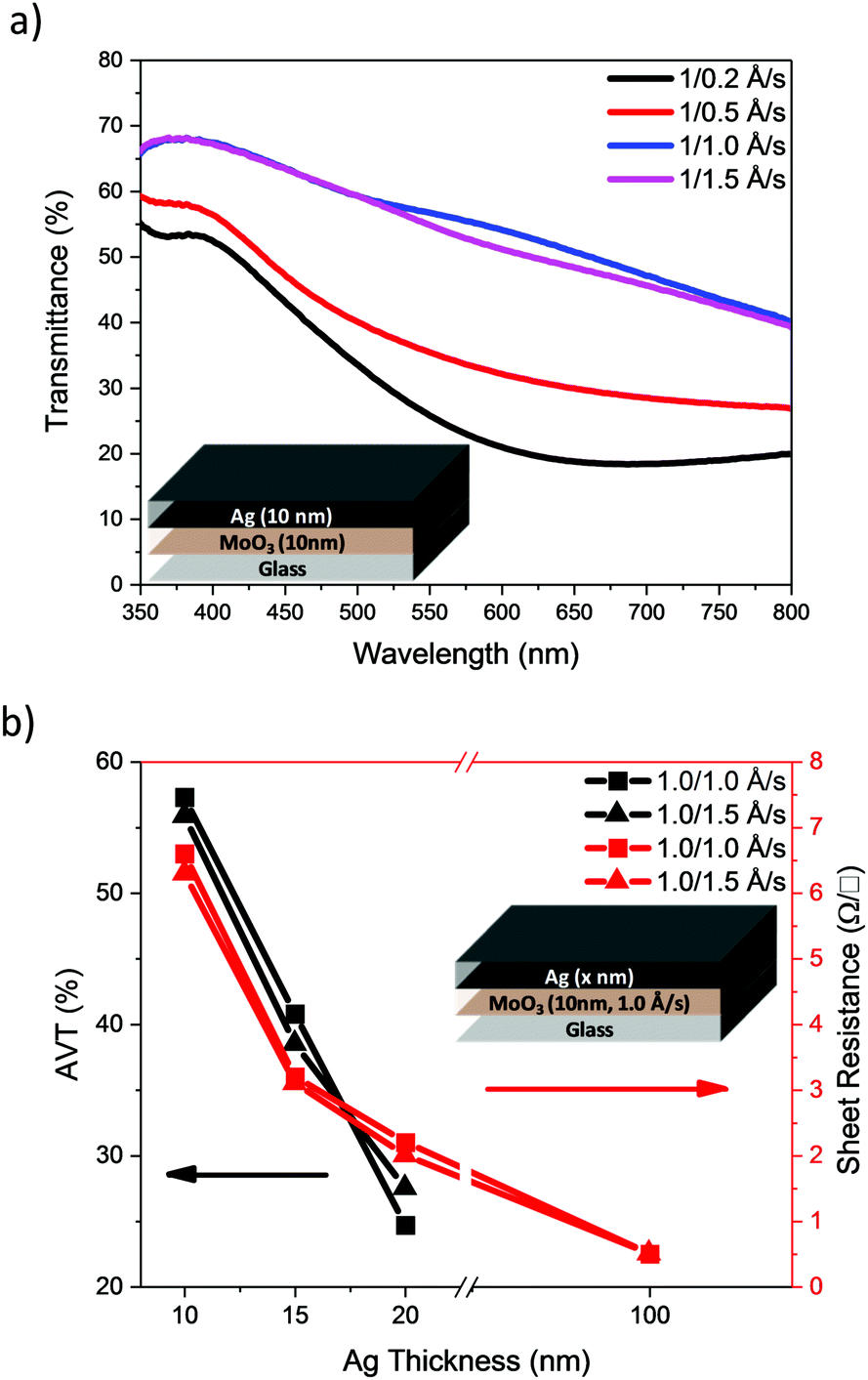 | ||
| Fig. 3 (a) Transmittance spectra of normal MoO3/Ag electrodes with 10 nm thick Ag and (b) electrode AVT and sheet resistance variation as a function of Ag film thickness. | ||
| Electrode structure | Deposition rates (MoO3/Ag) (Å s−1) | R sheet (Ω □−1) | AVT (%) | Images of electrodesb |
|---|---|---|---|---|
| a Sheet resistance measurement was not available because resistance value was out of the measurable range of instrument. b The rates in the image represent the deposition rates of the Ag film. | ||||
| 10/10 nm MoO3/Ag | 1/0.2 | N/Aa | 30.2 |
|
| 1/0.5 | 24.7 | 38.4 | ||
| 1/1.0 | 6.6 | 57.3 | ||
| 1/1.5 | 6.3 | 55.9 | ||
| 10/100 nm MoO3/Ag | 1/0.5 | 0.5 | N/A | N/A |
| ITO | N/A | 13 | N/A | N/A |
In order to understand the origin of the observed variations in performance, the microstructure of the electrodes was examined by SEM (Fig. 4). Looking initially at 10 nm Ag films deposited on 10 nm MoO3, the films as a function of deposition rate are shown in Fig. 4a. At low deposition rates (0.2 Å s−1), the Ag film grows in the form of isolated islands, giving a discontinuous morphology. The formation of such a discontinuous morphology is unfavourable for charge transport, resulting in the very high sheet resistance observed. As the deposition rate increases, agglomeration occurs across the Ag film. Increased connectivity between islands provides a continuous pathway for charge transport, improving the conductivity of the electrode. The change in Ag film morphology from isolated to inter-connected islands may also influence changes in the mode of any surface plasmons (SP) generated, resulting in a change from a localised SP to a propagating SP. Such changes have previously been proposed as an explanation for different transmittance values, and we hypothesise that similar effects may be occurring in our samples.17,20,21 The variation of sheet resistance with film thickness is likely due to similar effects, with increasing connectivity between islands occurring as the film thickness increases.17 Whilst increasing the thickness causes the formation of a uniform and dense film with reduced resistance, this results in a significant reduction in AVT.
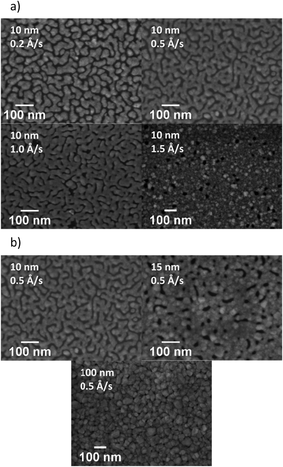 | ||
| Fig. 4 SEM images of Ag films with different (a) deposition rates and (b) thickness. | ||
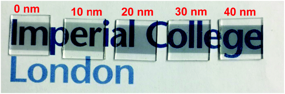
From the data presented in Table 1, a deposition rate of 1.5 Å s−1 was selected for Ag deposition in DMD structures. Focussing on films with 10 nm MoO3/10 nm Ag nm, DMD electrodes were fabricated with varying MoO3 thicknesses from 10 to 40 nm. The transmittance and reflectance spectra, recorded by illumination from the outer MoO3 side, are presented in Fig. 5. Similar measurements using 15 and 20 nm of Ag are shown in Fig. S2 and S3 (ESI†), from which the AVT and average visible reflectance (AVR) were calculated. Table 2 and Table S2 (ESI†) illustrate the optical and electrical characteristics of electrodes. They demonstrate that the sheet resistance of the DMD electrodes shows minor change as the outer MoO3 layer is varied, whereas their optical parameters are significantly influenced by the outer MoO3 layer. At a fixed 10 nm Ag thickness, the addition and increase in thickness of outer MoO3 significantly enhances the transmittance of electrodes and reduces the reflectance losses, consistent with the reported anti-reflective properties of MoO3.22 The images of electrodes, Table 2, highlight the significant improvements in transmittance observed with increased MoO3 thickness. Such a trend is consistent for the DMDs with either 10, 15 or 20 nm of Ag, and taken as a group it appeared that 30 or 40 nm of MoO3 would be optimal for subsequent device measurements. However preliminary measurement of the optical properties (Table S3 and Fig. S4, ESI†) of ST-OPV devices highlighted that those with 30 nm of outer MoO3 exhibited a larger optical asymmetry than those with 40 nm, with an undesirable difference in visual appearance when viewed from either electrode. As such we focussed on devices with a 40 nm outer layer for device characterisation.
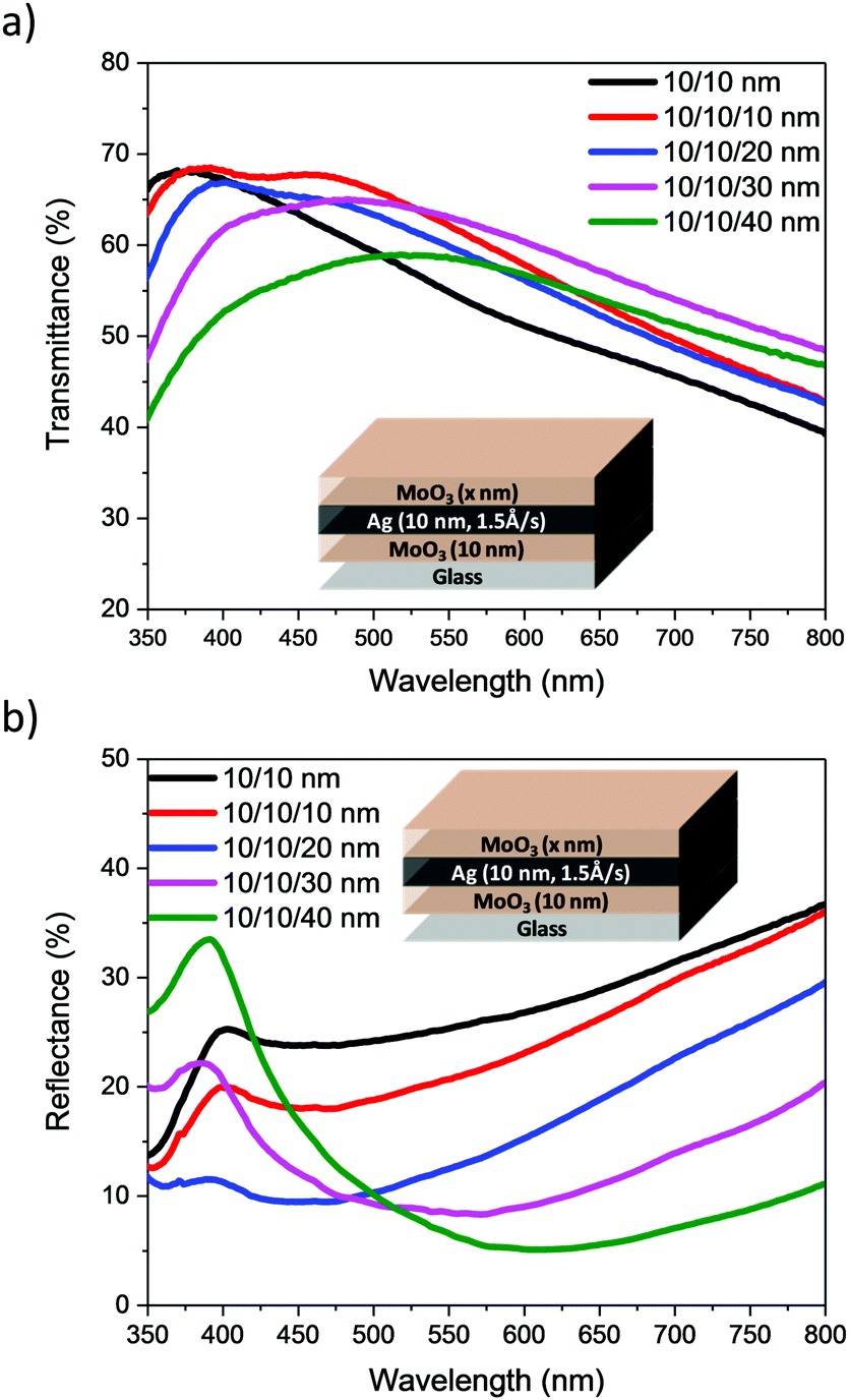 | ||
| Fig. 5 (a) Transmittance and (b) reflectance spectra of multilayer MoO3/Ag/MoO3 electrodes based on 10 nm (1.5 Å s−1) Ag film with different outer MoO3 film thickness (recorded with illumination from the MoO3 side). | ||
| Ag deposition rate | MoO3/Ag/MoO3 layer thicknesses (nm) | R sheet (Ω □−1) | AVT (%) | AVR (%) | Images of electrodes |
|---|---|---|---|---|---|
| 1.5 Å s−1 | 10/10 | 6.3 | 55.9 | 26.0 |
|
| 10/10/10 | 7.6 | 61.3 | 21.7 | ||
| 10/10/20 | 7.5 | 59.4 | 13.6 | ||
| 10/10/30 | 7.3 | 61.3 | 11.2 | ||
| 10/10/40 | 7.4 | 56.0 | 11.0 |
Using the optimised DMD structures, inverted architecture ST-OSC devices were fabricated were prepared with a general structure of ITO/ZnO/PFBDB-T:C8-ITIC/10 nm MoO3/Ag/40 nm MoO3 using either 10, 15 or 20 nm of Ag. As a reference, regular inverted architecture devices were also constructed with ITO/ZnO/PFBDB-T:C8-ITIC/10 nm MoO3/100 nm Ag.
The J–V characteristics of the ST-OSCs are given in Table 3 and shown in Fig. 6a. The reference opaque device exhibited similar performance to that previously reported,19 with an average PCE of 12.5%. The semi-transparent devices all exhibited similar open circuit voltage (Voc) and fill-factor (FF) to the reference device, but the short-circuit current (Jsc) was reduced. This reduction can be related to the reduced reflectivity of the HE electrode for the ST devices, which reduces the light intensity in the active layer. The Jsc also decreased as thinner Ag layers were used, likely as a result of the increase in Rsheet for these devices. The EQE spectra, Fig. 6b, show a good agreement with the measured Jsc values. The AVT values for the ST-OPV devices range from 19.1% to 23.5%. The transmittance required for a ST-OPV depends on the exact application, but it is generally suggested that an AVT of 20–30% would be the minimum requirement for window applications.4 Devices above the 20% AVT threshold exhibit average PCEs of 9.2 and 7.8%, and therefore appear potentially promising for these applications.
| Device electrodes | J sc (mA cm−2) | V oc (V) | FF | PCE (%) | R sheet (Ω □−1) | AVT (%) | AVR (%) | CIE (x,y) colour coordinates | |
|---|---|---|---|---|---|---|---|---|---|
| Topc | Botd | ||||||||
| a Values of devices with best performance. b Sheet resistance of top electrode. c Electrode side. d Glass side. | |||||||||
| 10/100 nm | 19.59 ± 1.11 | 0.93 ± 0.01 | 0.69 ± 0.00 | 12.5 ± 0.6 | 0.2 | N/A | N/A | N/A | |
| (1/1.5 Å s−1) | (21.07)a | (0.94)a | (0.70)a | (13.5)a | |||||
| 10/20/40 nm | 16.43 ± 0.47 | 0.92 ± 0.00 | 0.67 ± 0.01 | 10.0 ± 0.3 | 2.2 | 19.1 | 23.3 | 12.6 | (0.22,0.27) |
| (1/1.5/1 Å s−1) | (17.34)a | (0.92)a | (0.69) | (10.4)a | |||||
| 10/15/40 nm | 14.56 ± 0.51 | 0.92 ± 0.00 | 0.68 ± 0.01 | 9.2 ± 0.3 | 3.4 | 22.0 | 18.5 | 12.1 | (0.24,0.29) |
| (1/1.5/1 Å s−1) | (15.51)a | (0.92)a | (0.70)a | (9.8)a | |||||
| 10/10/40 nm | 13.06 ± 0.45 | 0.92 ± 0.01 | 0.67 ± 0.01 | 7.8 ± 0.3 | 7.4 | 23.5 | 10.3 | 13.6 | (0.25,0.29) |
| (1/1.5/1 Å s−1) | (13.90)a | (0.93)a | (0.67)a | (8.5)a | |||||
| Active layer | N/A | 40.1 | N/A | N/A | (0.23,0.28) | ||||
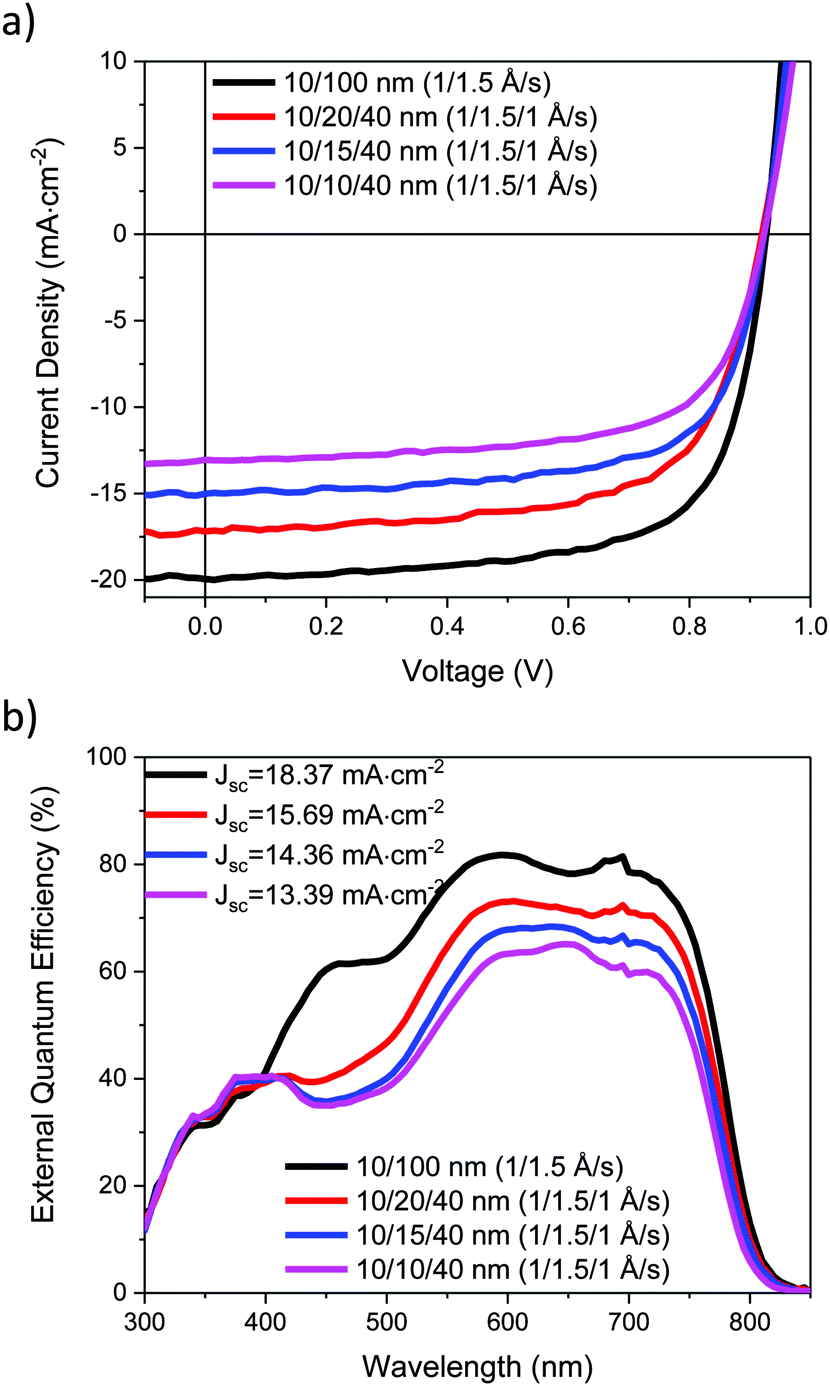 | ||
| Fig. 6 (a) J–V curves and (b) EQE spectra of the optimised ST-OSCs. | ||
Another important issue for window applications is the visual appearance of the cell. Hence the reflectance spectra from both sides of the devices were measured to investigate any optical asymmetry and the colour coordinates of the devices were calculated following the CIE protocol.12,13,23Table 3 shows the summary of device performance parameters. When considering the reflectance measured from both sides of the device, those prepared using 10/10/40 nm DMD electrodes exhibit an excellent optical symmetry. The colour coordinates of all devices stay in the blue region of the CIE 1931 chromaticity diagram and close to the coordinate of the active layer, indicating that the electrodes do not alter the colour defined by the active layer i.e. the light absorbing layer. Fig. 7b demonstrates the viewing taken through various ST-OSCs.
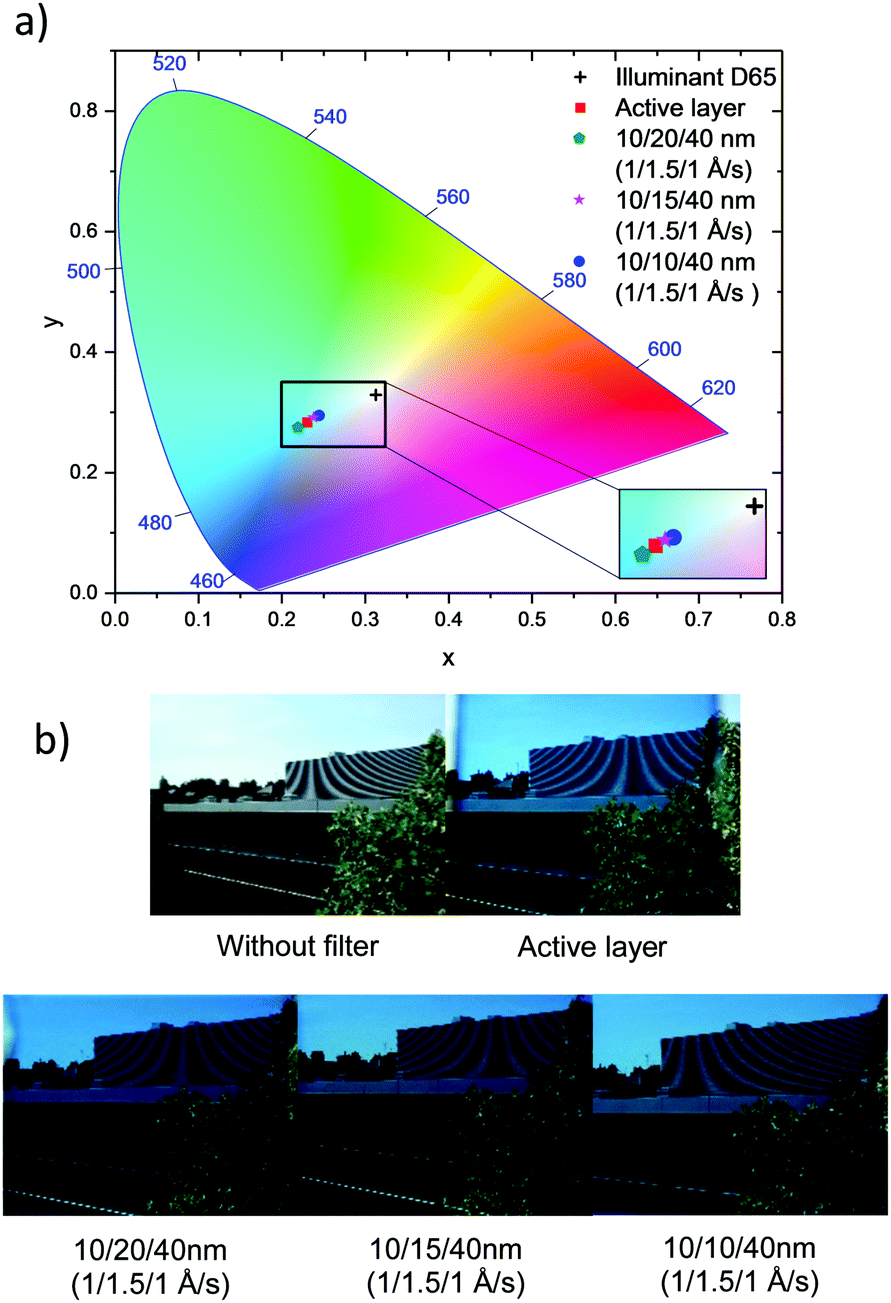 | ||
| Fig. 7 (a) Colour coordinates of the optimised ST-OSCs and active layers under standard D65 illumination on the CIE 1931 colour space and (b) images taken through different ST-OSCs. | ||
Conclusions
In summary, we report the influence that the rate of Ag deposition has on the electrical and optical performance of a bilayer MoO3/Ag electrode. We find that faster rates of silver deposition give reduced sheet resistance and improved transmittance in the visible region due to a change in the microstructure of the film, from isolated to inter-connected islands. Using the optimised Ag deposition rates, trilayer MoO3/Ag/MoO3 electrodes were fabricated and the optical and electrical performance was investigated as a function of Ag and MoO3 thickness. The sheet resistance is found to be independent of the outer MoO3 layer thickness, whereas transmittance and reflectance losses are strongly dependent. Using the optimal electrodes, semi-transparent photovoltaic devices were fabricated using a blend of a donor polymer (PFBDB-T) and a non-fullerene acceptor (C8-ITIC). Promising device performance was found with devices achieving an average PCE of 9.2% with an AVT of 22%.Conflicts of interest
There are no conflicts to declare.Acknowledgements
We thank the British Council (337323) and the Daphne Jackson Trust (supported by RSC and EPSRC) for financial support.Notes and references
- A. Colsmann, A. Puetz, A. Bauer, J. Hanisch, E. Ahlswede and U. Lemmer, Adv. Energy Mater., 2011, 1, 599–603 CrossRef CAS.
- C. J. M. Emmott, J. A. Röhr, M. Campoy-Quiles, T. Kirchartz, A. Urbina, N. J. Ekins-Daukes and J. Nelson, Energy Environ. Sci., 2015, 8, 1317–1328 RSC.
- R. R. Lunt and V. Bulovic, Appl. Phys. Lett., 2011, 98, 113305 CrossRef.
- Q. Xue, R. Xia, C. J. Brabec and H.-L. Yip, Energy Environ. Sci., 2018, 11, 1688–1709 RSC.
- J. Hou, O. Inganäs, R. H. Friend and F. Gao, Nat. Mater., 2018, 17, 119 CrossRef CAS PubMed.
- C. Yan, S. Barlow, Z. Wang, H. Yan, A. K. Y. Jen, S. R. Marder and X. Zhan, Nat. Rev. Mater., 2018, 3, 18003 CrossRef CAS.
- G. Zhang, J. Zhao, P. C. Y. Chow, K. Jiang, J. Zhang, Z. Zhu, J. Zhang, F. Huang and H. Yan, Chem. Rev., 2018, 118, 3447–3507 CrossRef CAS PubMed.
- K. Wang, C. Liu, T. Meng, C. Yi and X. Gong, Chem. Soc. Rev., 2016, 45, 2937–2975 RSC.
- J. H. Yim, S.-y. Joe, C. Pang, K. M. Lee, H. Jeong, J.-Y. Park, Y. H. Ahn, J. C. de Mello and S. Lee, ACS Nano, 2014, 8, 2857–2863 CrossRef CAS PubMed.
- K.-S. Chen, J.-F. Salinas, H.-L. Yip, L. Huo, J. Hou and A. K. Y. Jen, Energy Environ. Sci., 2012, 5, 9551–9557 RSC.
- K.-S. Lee, I. Kim, C. B. Yeon, J. W. Lim, S. J. Yun and G. E. Jabbour, ETRI J., 2013, 35, 587–593 CrossRef.
- M. B. Upama, M. Wright, N. K. Elumalai, M. A. Mahmud, D. Wang, K. H. Chan, C. Xu, F. Haque and A. Uddin, Curr. Appl. Phys., 2017, 17, 298–305 CrossRef.
- M. B. Upama, M. Wright, N. K. Elumalai, M. A. Mahmud, D. Wang, C. Xu and A. Uddin, ACS Photonics, 2017, 4, 2327–2334 CrossRef CAS.
- S. Kang, T. Kim, S. Cho, Y. Lee, A. Choe, B. Walker, S.-J. Ko, J. Y. Kim and H. Ko, Nano Lett., 2015, 15, 7933–7942 CrossRef CAS PubMed.
- C. Girotto, E. Voroshazi, D. Cheyns, P. Heremans and B. P. Rand, ACS Appl. Mater. Interfaces, 2011, 3, 3244–3247 CrossRef CAS PubMed.
- X. Tian, Y. Zhang, Y. Hao, Y. Cui, W. Wang, F. Shi, H. Wang, B. Wei and W. Huang, J. Nanophotonics, 2015, 9, 093043 CrossRef.
- W.-F. Xu, C.-C. Chin, D.-W. Hung and P.-K. Wei, Sol. Energy Mater. Sol. Cells, 2013, 118, 81–89 CrossRef CAS.
- Y. Lin, J. Wang, Z.-G. Zhang, H. Bai, Y. Li, D. Zhu and X. Zhan, Adv. Mater., 2015, 27, 1170–1174 CrossRef CAS PubMed.
- Z. Fei, F. D. Eisner, X. Jiao, M. Azzouzi, J. A. Röhr, Y. Han, M. Shahid, A. S. R. Chesman, C. D. Easton, C. R. McNeill, T. D. Anthopoulos, J. Nelson and M. Heeney, Adv. Mater., 2018, 30, 1705209 CrossRef PubMed.
- S. H. Oh, S.-M. Lee and K. C. Choi, Thin Solid Films, 2012, 520, 3605–3608 CrossRef CAS.
- K. H. Cho, S. I. Ahn, S. M. Lee, C. S. Choi and K. C. Choi, Appl. Phys. Lett., 2010, 97, 193306 CrossRef.
- W.-H. Park, G.-N. Lee and J. Kim, Sens. Actuators, A, 2018, 271, 251–256 CrossRef CAS.
- R. W. G. Hunt and M. R. Pointer, Measuring Color, John Wiley & Sons, 4th edn, 2011 Search PubMed.
Footnote |
| † Electronic supplementary information (ESI) available. See DOI: 10.1039/c8qm00610e |
| This journal is © the Partner Organisations 2019 |