
UV-enhanced NO2 gas sensing properties of polystyrene sulfonate functionalized ZnO nanowires at room temperature
Jing
Wang
 *a,
Mingying
Yu
a,
Xian
Li
b and
Yi
Xia
c
*a,
Mingying
Yu
a,
Xian
Li
b and
Yi
Xia
c
aThe Key Laboratory of Synthetic and Biological Colloids, Ministry of Education, School of Chemical and Material Engineering, Jiangnan University, Wuxi 214122, China. E-mail: jingwang@jiangnan.edu.cn
bAgricultural Information Institute, Chinese Academy of Agricultural Sciences, Key Laboratory of Agricultural Information Service Technology of Ministry of Agriculture, Beijing 100081, China
cResearch Center for Analysis and Measurement, Kunming University of Science and Technology, Kunming 650093, China
First published on 15th November 2018
Abstract
Polystyrene sulfonate (PSS) functionalized ZnO nanowires were hydrothermally synthesized and assembled into a UV-activated optoelectronic NO2 sensor for the first time. In situ PSS functionalization during hydrothermal synthesis not only facilitated the formation of high-quality ZnO nanowires with small diameters and high aspect ratios, but also significantly improved the UV photoconductance of ZnO nanowires through photo-induced electron injection, leading to the enhanced optoelectronic properties of ZnO nanowires. The optoelectronic NO2 sensors based on PSS-functionalized ZnO nanowires showed much higher responses and faster response rates under UV illumination at room temperature (25 °C). The responses ranged from 60% to 690% toward NO2 concentrations of 50 ppb to 2 ppm. Moreover, the optoelectronic sensors exhibited excellent reversibility, good stability and a low detection limit (5 ppb), making the efficient, optically controlled sensing of ppb-level NO2 gas possible.
1. Introduction
The detection of nitrogen dioxide (NO2) has been a long-term important issue, since NO2 is one of the most toxic gaseous pollutants that affects human health at a ppm level and also causes acid rain.1 Gas sensors based on metal oxide nanomaterials offer multiple advantages including low cost, high responses, potential for miniaturization and operational simplicity.2 In particular, ZnO nanostructures have been widely employed as NO2 sensing materials due to their high sensitivity and selectivity to NO2.3,4 However, traditional NO2 sensors based on metal oxide nanomaterials usually operate at high temperatures (typically 150–600 °C), which causes problems such as energy consumption, short sensor life, and the difficulty of being integrated with flexible devices.5 These limitations have motivated researchers to become engaged in the fabrication of room-temperature NO2 sensors. Recently, ZnO-based room-temperature NO2 sensors employing UV activation have attracted intensive research interest due to the excellent optoelectronic properties of ZnO in the UV region.6–8 UV illumination leads to the photogeneration of free charge carriers in ZnO, which not only increases the material conductivity, but also promotes the surface adsorption/desorption of gas molecules, thus improving both the sensor sensitivity and response/recovery speed.In order to further satisfy the practical applications of room-temperature NO2 sensors, many efforts have been devoted to improving the optoelectronic sensing performance of ZnO nanostructures. To date, mainly two effective strategies including morphology modulation and surface functionalization have been developed. On the one hand, successful attempts have been reported to improve the morphology-dependent optoelectronic properties by modulating ZnO nanostructures with tailored size, dimensions or microstructures.9–12 Particularly, one-dimensional ZnO nanostructures have been demonstrated as promising candidates for multifunctional optoelectronic devices owing to their large surface-to-volume ratios, high electron mobility and excellent device interconnecting ability.11,12 On the other hand, improved optoelectronic NO2 sensing properties have been achieved by surface functionalization of ZnO nanowires with various light-active materials, such as other semiconducting materials,13–15 noble metal nanoparticles16,17 or light-absorbing dyes and polymers.18,19 These surface modifiers significantly increase the free electrons in ZnO under light illumination through photo-induced charge separation and transfer processes; thus the number of electrons that participate in the surface reaction with NO2 molecules greatly increase, leading to the enhanced optoelectronic sensing performances.
In this work, polystyrene sulfonate (PSS) functionalized ZnO nanowires were hydrothermally synthesized and fabricated into a UV-activated optoelectronic NO2 sensor for the first time. The in situ PSS functionalization during hydrothermal synthesis facilitated the formation of high-quality ZnO nanowires with small diameters and high aspect ratios, serving as ideal sensing materials for optoelectronic devices. More importantly, the surface adsorbed PSS significantly improve the UV photoconductance of ZnO nanowires through photo-induced electron injection, leading to the enhanced optoelectronic properties of ZnO nanowires. Owing to the dual roles of PSS functionalization, the room-temperature NO2 sensors based on PSS-functionalized ZnO nanowires exhibited a highly sensitive, fast, reversible and stable optoelectronic response under UV illumination, making the efficient, optically controlled sensing of ppb-level NO2 gas possible.
2. Experimental
2.1 Synthesis
Commercial chemicals of analytical grade were used in all the experiments. ZnO nanowires were synthesized by hydrothermal hydrolysis of zinc alkaline solutions using ZnO and NaOH as the starting chemicals. First, 100.0 mL of a transparent zinc alkaline solution was prepared by dissolving 4.07 g of ZnO and 30.00 g of NaOH in water. Then, 8.0 mL of the solutions were diluted with 32.0 mL of water to form solutions containing 0.1 mol L−1 [Zn2+] and 1.5 mol L−1 [OH−], and 0.1 g sodium polystyrene sulfonate was dissolved in the solution. This stock solution was hydrothermally treated at 140 °C for 4.0 h. The obtained white precipitates were filtered, washed, and dried at 60 °C for 24 h.2.2 Materials characterization
Powder X-ray diffraction (XRD) was used for phase identification using an X-ray diffractometer (D8 Advance, Bruker, Germany) with CuKα (λ = 0.154178 nm) radiation. The morphology and microstructures of the samples were examined with a field emission scanning electron microscope (FESEM, JSM 7401F, JEOL, Japan) and a high-resolution transmission electron microscope (HRTEM, JEM-2010, JEOL, Japan), respectively. The functional groups of the samples were examined by using a Fourier transform infrared spectrometer (FT-IR, Nexus, Nicolet, USA). The surface compositions of the samples were determined by using an X-ray photoelectron spectrometer (XPS, PHI-5300, PHI, USA). UV-vis-NIR diffuse reflectance spectra were recorded on a PerkinElmer Lambda 950 UV-vis-NIR spectrophotometer. Room temperature photoluminescence (PL) spectra of the samples were recorded on a Hitachi F-7000 luminescence spectrometer using a Xe lamp with an excitation wavelength of 325 nm.2.3 Sensor device fabrication and measurements
An N-type (100) oriented silicon wafer with a 300 nm thick SiO2 dielectric-layer was used as the device substrate. The inter-digital electrodes with a finger width of 10 μm and a gap width of 10 μm were patterned by standard photolithography and the titanium/gold (Ti/Au, 20 nm/100 nm) electrodes were deposited by RF sputtering and a lift-off process. ZnO samples were dispersed in ethanol to achieve a concentration of 3.0 g L−1 and sonicated for 20 min. The suspension was spin-coated onto interdigitated electrodes and dried at 60 °C to obtain the sensor devices. The effective illuminated area of the sensor was ca. 30 mm2. The UV source used in the experiment had a wavelength distribution of around 280 nm. The illumination power was adjusted using an optical attenuator and was measured by using a power meter. The optoelectronic properties of the devices were determined using a Keithley 2700 SourceMeter. All measurements were performed in air at 25 °C.The sensing tests were performed in a homemade chamber with dry air as the carrier gas at 25 °C unless otherwise specified. The input concentration of NO2 was 2 ppb to 2 ppm and the flow rate of the mixed gas was 200 mL min−1. The resistance of the films was measured in the dark or under UV illumination and recorded by using a Keithley 2700 multimeter/data acquisition system. The response (R) of the sensor is defined as  , where Ra is the initial resistance in dry air, and Rg is the resistance of the device after being exposed to a NO2 atmosphere. The response time is defined as the time required until 90% of the whole response is reached while the recovery time denotes the time needed until 90% of the signal is recovered.
3. Results and discussion
3.1 Hydrothermal synthesis of PSS-functionalized ZnO nanowires
The effects of in situ PSS functionalization on the hydrothermal formation of ZnO nanowires were first studied. Fig. 1a and b show the SEM images of the products obtained in the absence or presence of PSS, and their statistical diameter distributions are presented in Fig. 1c. Nonuniform ZnO microwires with lengths of 20–50 μm and a broad diameter distribution ranging from 100 nm to 5 μm were obtained from bare zinc-alkaline solutions (denoted as ZnO-blank). With the addition of PSS, the diameters of the nanowires sharply decreased to 50–300 nm while the lengths remained almost the same, thus producing uniform nanowires with a high aspect ratio over 200 (denoted as ZnO–PSS). A typical XRD pattern of ZnO–PSS (Fig. 1d) displays the sharp diffraction peaks of ZnO, indicating the high-crystallinity of the nanowires. The HRTEM image showing a d-spacing of 0.26 nm and the corresponding SAED pattern revealed the c-axis oriented growth and single-crystal nature of the nanowires (insets in Fig. 1d). These results indicated that PSS played a key role in promoting the anisotropic growth of ZnO nanowires with small diameters and high aspect ratios. | ||
| Fig. 1 SEM images of ZnO–blank (a) and ZnO–PSS (b); (c) statistical diameter distribution of the nanowires; and (d) typical XRD pattern of ZnO–PSS; insets: HRTEM image and SAED pattern. | ||
The anisotropic growth of inorganic nanostructures under hydrothermal conditions was usually considered as a kinetically controlled process.20 In our experiments, it was observed that the growth rate of ZnO in the presence of PSS was significantly lowered, implying that the growth of ZnO was hindered by PSS. Such growth suppression was widely observed and attributed to the adsorption of the organic ligands at the crystal–solution interface.21 Moreover, these organic ligands could exert a highly selective effect, acting on certain crystallographic faces and thus directing the anisotropic growth of nanostructures.21 In the current case, we suggest that the PSS molecules may selectively adsorb on the (100) prism planes rather than on the (001) polar planes of ZnO, inhibiting their radial growth and thereby promoting the anisotropic growth of nanowires along the c-axis. The adsorption of PSS onto ZnO surfaces was examined by FT-IR analyses, as shown in Fig. 2. Compared with the IR curve of uncapped ZnO, some new peaks occurred in ZnO synthesized in the presence of PSS. The peaks at 2852 cm−1 and 2922 cm−1 were attributed the stretching vibrations of –CH2–. The peak at 1633 cm−1 attributable to the stretching of C![[double bond, length as m-dash]](https://www.rsc.org/images/entities/char_e001.gif) C in the aromatic rings of PSS was also observed for the ZnO–PSS sample. The two peaks at 1173 cm−1 and 1095 cm−1 could be assigned to the two stretching vibration modes of SO, νas(SO3) and νs(SO3), respectively, which shifted to the lower wavelength compared to those in free sulfonate groups (1180 and 1124 cm−1),22 implying the strong interactions of sulfonate groups in PSS with ZnO surfaces.
C in the aromatic rings of PSS was also observed for the ZnO–PSS sample. The two peaks at 1173 cm−1 and 1095 cm−1 could be assigned to the two stretching vibration modes of SO, νas(SO3) and νs(SO3), respectively, which shifted to the lower wavelength compared to those in free sulfonate groups (1180 and 1124 cm−1),22 implying the strong interactions of sulfonate groups in PSS with ZnO surfaces.
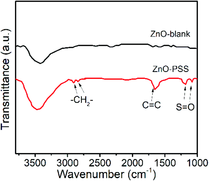 | ||
| Fig. 2 FT-IR spectra of ZnO–blank and ZnO–PSS. | ||
XPS spectra were further employed to study the surface structures of PSS-functionalized ZnO to identify the adsorption mechanisms, as shown in Fig. 3. Additional S 2p and Na 1s peaks were detected in the survey spectra (Fig. 3a). The high evolution S 2p peak of ZnO–PSS could be divided into two peaks centered at 168.9 and 167.7 eV (Fig. 3b), corresponding to the S 2p1/2 and S 2p3/2 transitions, respectively, which were quite identical to those in ZnSO3,23 suggesting the interaction between the –SO3 groups in PSS and the zinc ions on ZnO surfaces. For zinc-related species, Zn L3M45M45 Auger electron spectra (AES) were recorded since they were quite sensitive to the structural variations (Fig. 3c). The peaks at 497.7 and 494.3 eV could be assigned to the lattice Zn2+ and the zinc interstitials,24 respectively, while the additional peak centered at 496.3 eV should have originated from the surface zinc ions interacting with the PSS molecules. The above FT-IR and XPS analyses implied that the PSS molecules may serve as a surface ligand, with their sulfonate groups coordinating with the surface Zn2+ ions forming Zn–SO3 complexes. It was noticed that the anionic polymer functionalized ZnO nanostructures were generally prepared by electrostatic layer-by-layer assembly, with the assistance of positively charged polymers as intermediate layers, by considering the negatively charged surface of ZnO in aqueous solution.25 In contrast, herein, in situ PSS functionalization was carried out during the hydrothermal synthesis based on a surface ligand adsorption mechanism. Such an in situ functionalization method not only avoids the multistep assembly procedures and the use of other additives, but also renders a robust contact between ZnO and PSS, which is beneficial for the charge transfer in optoelectronic processes.
 | ||
| Fig. 3 XPS spectra of ZnO–PSS: (a) survey curve; (b) high-resolution S 2p peak and (c) Zn L3M45M45 Auger peak. | ||
3.2 Optical and optoelectronic properties
UV-vis absorption and room-temperature photoluminescence (PL) spectroscopy was employed to characterize the optical properties of the samples, which are closely related to the optoelectronic performances. As shown in Fig. 4a, the ZnO-blank sample exhibited an exciton absorption peak located at 373 nm, corresponding to the band gap of ZnO (3.3 eV). The absorption of ZnO–PSS in the UV region was significantly enhanced compared to that of ZnO-blank, since an additional peak of high intensity centered around 260 nm appeared, which derived from the UV-absorbing PSS. For the PL spectra (Fig. 4b), both ZnO samples consisted of two emission bands: a sharp emission in the UV region and a broad band in the visible range (400–700 nm). The narrow UV emission centred at ca. 386 nm originates from the excitonic recombination of electrons near the conduction band with holes near the valence band, while the green emission centered at ca. 540–550 nm is generally assigned to the surface defect-mediated emission.26 It was observed that the uncapped ZnO showed a weak UV emission but a strong green emission, indicating the existence of abundant surface defects in the ZnO-blank sample. The intensity of UV emission was enhanced by over one order of magnitude when the ZnO nanowires were functionalized with PSS, while the intensity of the green emission decreased drastically, demonstrating the improved optical properties of the ZnO nanowires owing to the surface passivation effects of PSS.27,28 Such PSS-functionalized ZnO nanowires with significantly improved optical properties were expected to exhibit better performances in optoelectronic devices. | ||
| Fig. 4 (a) The UV-Vis spectra and (b) room-temperature photoluminescence spectra of ZnO–blank and ZnO–PSS. | ||
The as-prepared ZnO nanowires were constructed into optoelectronic devices to investigate their electric transport properties at 25 °C under UV illumination. Fig. 5a and b present the current–voltage (I–V) characteristics of the devices based on ZnO-blank and ZnO–PSS, respectively, under dark and UV illumination conditions (λ ∼ 254 nm, P = 5 × 10⁻⁴ W cm−2). Both samples exhibited linear I–V characteristics, indicating good ohmic contacts between the nanowire films and electrodes.29 At an applied voltage of 5.0 V, the dark currents across ZnO-blank and ZnO–PSS were 2.49 μA and 0.87 μA, respectively. The suppressed dark current of ZnO–PSS could be attributed to the narrowed conducting channel induced by the thinner diameter, and the barrier effects of surface-absorbed PPS (considering that the PSS polymer itself is almost nonconductive). Under UV illumination, the current across the ZnO–PSS sample drastically increased to 212 μA, which was much higher than that of the ZnO-blank sample (14 μA), indicating that the PSS functionalization greatly improved the photoconductance of the ZnO nanowires. Due to the suppressed dark current and enhanced photoconductance, the PSS-functionalized ZnO nanowires exhibited a high UV-to-dark signal ratio of ∼240, being over 40 times larger than that of the ZnO-blank sample (IUV/Idark = 5.6). The enhanced UV photoconductance of the PSS-functionalized ZnO nanowires could be attributed to the charge transfer between PSS and ZnO under UV illumination, as illustrated schematically in Fig. 5c. Since the absorption peak of PSS is very close to the 254 nm UV source used in this study, it is expected that under UV illumination, electrons in PSS are excited from the highest occupied molecular orbital (HOMO) to its lowest unoccupied molecular orbital (LUMO), and then they are injected into the conduction band of ZnO. It is also possible that the electron in the valence band of ZnO is likely to be excited to the HOMO of PSS. Such a “hopping” process may enhance the transition probability of the valence electrons in ZnO to its conduction band, thus largely increasing the number of photogenerated charge carriers in ZnO.25,30 In addition, since the surface defects of ZnO were reduced by PSS functionalization (as revealed by PL analyses), the defect mediated recombination of electrons and holes could be greatly inhibited, which may also contribute to the enhanced optoelectronic performance of PSS-functionalized ZnO nanowires.
 | ||
| Fig. 5 Current–voltage (I–V) characteristics of the devices based on ZnO-blank (a) and ZnO–PSS (b) under dark and UV illumination conditions (λ ∼ 254 nm, P = 5 × 10⁻⁴ W cm−2); and (c) schematic illustration of the charge transfer process in PSS-functionalized ZnO nanowires. | ||
Based on the above experimental results, the roles of PPS functionalization in enhancing the optoelectronic performances of ZnO nanowires could be summarized by the following two aspects. On the one hand, the PSS molecules may adsorb preferentially onto the (100) prism planes of ZnO nanowires through sulfonate groups coordinating with surface zinc ions, thus hindering the radial growth and thereby leading to the formation of nanowires with thinner diameters and high aspect ratios. On the other hand, the energy levels introduced by PSS could be coupled with ZnO, serving as “hopping” states that promote the injection of electrons into the conduction band of ZnO under UV illumination. Therefore, a significant enhancement of the optoelectronic performance of ZnO nanowires was achieved. Although both the roles of polymers in directing the ZnO nanowire growth and improving the optoelectronic properties of ZnO–polymer hybrids have been previously reported, our current work reports for the first time that the UV-absorbing PSS polymer could play dual roles in enhancing the optoelectronic properties of ZnO nanowires.
3.3 Optoelectronic NO2 sensing properties
In this work, PSS-functionalized ZnO nanowires were constructed into a UV-activated optoelectronic NO2 sensor for the first time. We compared the NO2 sensing properties of the ZnO-blank and ZnO–PSS samples at 25 °C in the dark and under UV illumination (λ = 254 nm, P = 5 × 10⁻⁴ W cm−2); and the variations of resistances of the sensing film exposed to 2.0 ppm of NO2 are shown in Fig. 6a and b. Under dark conditions, the ZnO–PSS sample exhibited a high base resistance (5.70 MΩ) due to the barrier effects of PSS and the narrowed conducting channel; however, the resistance of the ZnO–PSS sample became even higher (12.03 MΩ) after exposure to NO2, exhibiting a response of 112% to 2 ppm of NO2, which was about 4 times larger than that of ZnO-blank (29%). The enhanced response could be reasonably explained by the significantly reduced diameters of the PSS-functionalized ZnO nanowires. However, both samples exhibited slow sensing dynamics, with similar response and recovery times being ca. 300 s and 440 s, respectively. A significant reduction of the electrical resistance of the sensing films was observed after UV illumination, and the ZnO–PSS sample showed a much smaller resistance of 0.018 MΩ compared to that of the blank-ZnO sample (0.36 MΩ), owing to the electron-injection by PSS. Upon NO2 exposure, the resistance of the films based on blank-ZnO and ZnO–PSS increased to 0.61 and 0.138 MΩ, respectively. Hence, the response of ZnO-blank increased to 70% upon UV activation; meanwhile the response and recovery times were reduced to 81.5 s and 91 s, respectively. For the ZnO–PSS sample, the UV activation led to the dramatic increase of the response to ca. 690%, and the further decrease of the response time to 29.5 s (but the recovery time was not obviously decreased). These results indicated that the PSS functionalization could significantly improve the sensor response and sensing rate. The enhanced optoelectronic NO2 sensing should be attributed to the increased carrier density in ZnO nanowires due to electron injection from PSS under UV illumination, and thus the number of electrons that participate in the reaction with NO2 gas molecules greatly increased. The influence of the light intensity on gas sensing properties was also investigated. Fig. 6c shows the responses of ZnO–PSS to 2 ppm of NO2versus the change of the light intensity from 5 × 10⁻⁵ W cm−2 to 2 × 10⁻³ W cm−2. It was observed that the response tended to saturate with the increase of the light intensity. These results could be attributed to the fact that a limited quantity of photogenerated electrons would participate in the surface adsorption of NO2, while excessive photogenerated carriers may hinder the adsorption process.31 In the current case, a light intensity of 5 × 10⁻⁴ W cm−2 was found to be most favorable for achieving the highest response.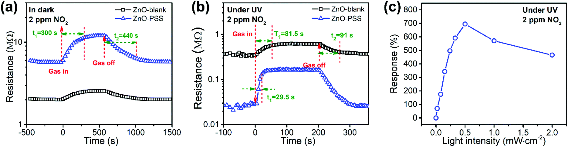 | ||
| Fig. 6 (a, b) Dynamic response curves of the sensors based on ZnO-blank and ZnO–PSS to 2 ppm of NO2: (a) in the dark and (b) under UV illumination; and (c) response of the sensor based on ZnO–PSS versus light intensity (2 ppm of NO2). | ||
The optoelectronic NO2 sensing performance of the PSS-functionalized ZnO nanowires was further evaluated at 8 different concentrations of NO2 ranging from 50 ppb to 2 ppm under UV light illumination (bias = 5.0 V, 5 × 10⁻⁴ W cm−2), as shown in Fig. 7a. One can see that the response increases quickly upon NO2 exposure and the response gradually decreases to the base line when NO2 is switched off, demonstrating excellent reversible response and recovery properties upon continuous NO2 exposure/release cycles. The ZnO–PSS based optoelectronic gas sensor shows responses ranging from 60% to 690% toward NO2 concentrations ranging from 50 ppb to 2 ppm. Fig. 7b shows the responses of the sensor as a function of NO2 concentrations. The data can be fitted well with the Langmuir adsorption isotherm, R = a/(1 + b/C), where C represents the concentration of NO2, which was further confirmed by the linear fitting of R−1versus C−1 (inset of Fig. 7b). These results can be understood as the surface coverage of NO2 molecules follows the Langmuir adsorption isotherm. At lower concentrations, the sensor exhibits an approximately linear relationship between the sensor response and the gas concentration because the surface adsorption sites are not saturated. At higher concentrations, the surface coverage tends to saturate and hence leads to the saturation response.32,33 The dynamic response curves measured at very low concentrations of NO2 revealed a clear response of ca. 4.5% to 5 ppb of NO2, which was considered as the detection limit of NO2. In comparison, the ZnO-blank sample did not show any obvious response to 20 ppb of NO2. Such a low detection limit of PSS-functionalized ZnO nanowires is beneficial for their practical application in NO2 sensors. In addition, Fig. 7d shows the responses of the sensor to 2 ppm of NO2 and other gases including NO, SO2, Cl2, HCHO, H2S, NH3 and CO, which are typical oxidative or reductive air pollutants. Obviously, the ZnO–PSS optoelectronic sensor exhibited very high selectivity to NO2.
 | ||
| Fig. 7 Dynamic response curves (a) and responses (b) of the sensor based on ZnO–PSS upon exposure to NO2 with concentrations ranging from 50 ppb to 2 ppm under UV illumination; inset in b: 1/response versus 1/c with linear line fitting; (c) dynamic response curves of the sensor based on ZnO–PSS upon exposure to 2–10 ppb of NO2 under UV illumination; and (d) responses of the sensor based on ZnO–PSS to 2 ppm of NO2 and other gases. | ||
In order to confirm the repeatability of the optoelectronic NO2 sensor, the time dependent photoresponse of the sensor in air or in 2 ppm of NO2 was tested by periodically turning on and off the UV light, as shown in Fig. 8a. It was observed that the sensor could work once light was illuminated and it was repeatable. The excellent optoelectronic properties of ZnO–PSS were favorable for the instant, optically controlled sensing of NO2 since the photoresponse was fast and the photocurrent was quite stable and repeatable. The sensor was also exposed to 2 ppm of NO2 for 6 successive exposure/release cycles (Fig. 8b). Stable responses of 670–700% were observed in 6 cycles with little appreciable baseline drift, demonstrating good reproducibility of the sensor. Furthermore, we checked the long-time stability of the sensor in air to find more practical application capability. The dynamic response curves of the sensor after 30 and 90 days’ storage are presented in Fig. 8c. After 90 days in air, the sensor could still accomplish effective detection with fast response and almost full recovery, and a response of 590% to 2 ppm of NO2 was achieved, indicating that ca. 85% of the initial response could be retained. The effect of the relative humidity (RH) on the sensor response of the ZnO–PSS sample was also studied, as shown in Fig. 8d, which is very important for a room-temperature gas sensor. It was found that the sensor response decreased with increasing RH, which should be attributed to the adsorption of water molecules that inhibited the adsorption of O2 and NO2. However, at a high RH of 80%, a sensor response of ca. 410% could still be achieved. The result indicated that although the sensing performance of the optoelectronic sensor showed a degradation at high RH, it could still meet the demand of NO2 detection. To sum up, owing to the dual roles of PSS functionalization, the room-temperature NO2 sensors based on PSS-functionalized ZnO nanowires exhibited a highly sensitive, fast, reversible and stable optoelectronic response under UV illumination, making the efficient, optically controlled sensing of ppb-level NO2 gas possible. The presently developed in situ functionalization approach also provides an alternative strategy for the design and construction of metal oxide/polymer nanocomposites, which opens a facile pathway to the fabrication of high-performance room-temperature NO2 sensors.
 | ||
| Fig. 8 (a) Time dependent photoresponse in air and in 2 ppm of NO2 by periodically turning on and off the UV light; (b) reproducibility of the ZnO–PSS sensor exposed to 2 ppm of NO2 under UV illumination (for 6 successive cycles); (c) dynamic response curve of the sensor to 2 ppm of NO2 after 30 and 90 days’ storage; and (d) effect of the relative humidity on the response of the ZnO–PSS sensor to 2 ppm of NO2 under UV illumination. | ||
4. Conclusion
In summary, polystyrene sulfonate (PSS) functionalized ZnO nanowires have been synthesized by a hydrothermal method. The PSS-functionalized ZnO nanowires were constructed into an optoelectronic NO2 sensor and its resulting responses ranged from 60% to 690% toward NO2 concentrations of 50 to 2000 ppb. The remarkable improvement in the gas sensing performances under UV illumination was attributed to the dual role of in situ PSS functionalization. On the one hand, the surface adsorption of PSS promoted the formation of high-quality ZnO nanowires with small diameters and high aspect ratios; on the other hand, the PSS functionalization significantly increased the photo-induced carrier density in ZnO nanowires through electron injection, and thus the number of electrons that participate in the reaction with NO2 gas molecules greatly increased. The as-fabricated electronic NO2 sensors were particularly attractive for their excellent reversibility, good stability, high selectivity and low detection limits, making the efficient, optically controlled sensing of ppb-level NO2 gas possible.Conflicts of interest
There are no conflicts to declare.Acknowledgements
This work was supported by the National Natural Science Foundation of China (No. 51802123), the Natural Science Foundation of Jiangsu Province (No. BK20180630) and the Fundamental Research Funds for the Central Universities (JUSRP11816).References
- J. A. Bernstein, N. Alexis, C. Barnes, I. L. Bernstein, J. A. Bernstein, A. Nel, D. Peden, D. Diaz-Sanchez, S. M. Tarlo and P. B. Williams, J. Allergy Clin. Immunol., 2004, 114, 1116–1123 CrossRef PubMed.
- D. Miller, S. Akbar and P. Morris, Sens. Actuators, B, 2012, 204, 250–272 CrossRef.
- R. Kumar, O. Al-Dossary, G. Kumar and A. Umar, Nano-Micro Lett., 2015, 7, 97–120 CrossRef PubMed.
- M. Chen, Z. Wang, D. Han, F. Gu and G. Guo, J. Phys. Chem. C, 2011, 115, 12763–12773 CrossRef CAS.
- J. Zhang, X. Liu, G. Neri and N. Pinna, Adv. Mater., 2016, 28, 795–831 CrossRef CAS PubMed.
- T. Wu, Z. Wang, M. Tian, J. Miao, H. Zhang and J. Sun, Sens. Actuators, B, 2018, 259, 526–531 CrossRef CAS.
- Y. Su, G. Xie, H. Tai, S. Li, B. Yang, S. Wang, Q. Zhang, H. Du, H. Zhang, X. Du and Y. Jiang, Nano Energy, 2018, 47, 316–324 CrossRef CAS.
- X. Su, L. Gao, F. Zhou, W. Cai and G. Duan, RSC Adv., 2017, 7, 21054–21060 RSC.
- Y. Mishra, G. Modi, V. Cretu, V. Postica, O. Lupan, T. Reimer, I. Paulowicz, V. Hrkac, W. Benecke, L. Kienle and R. Adelung, ACS Appl. Mater. Interfaces, 2015, 7, 14303–14316 CrossRef CAS PubMed.
- C. Xiao, T. Yang, M. Chuai, B. Xiao and M. Zhang, Phys. Chem. Chem. Phys., 2016, 18, 325–330 RSC.
- G. Lu, J. Xu, J. Sun, Y. Yu, Y. Zhang and F. Liu, Sens. Actuators, B, 2012, 162, 82–88 CrossRef CAS.
- S. Park, S. An, Y. Mun and C. Lee, ACS Appl. Mater. Interfaces, 2013, 10, 4285–4292 CrossRef PubMed.
- Y. Zhou, C. Gao and Y. Guo, J. Mater. Chem. A, 2018, 6, 10286–10296 RSC.
- R. Chen, J. Wang, Y. Xia and L. Xiang, Sens. Actuators, B, 2018, 255, 2538–2545 CrossRef CAS.
- E. Espid and F. Taghipour, Sens. Actuators, B, 2017, 241, 828–839 CrossRef CAS.
- N. Gogurla, A. K. Sinha, S. Santra, S. Manna and S. K. Ray, Sci. Rep., 2014, 4, 6483 CrossRef CAS PubMed.
- Q. Zhang, G. Xie, M. Xu, Y. Su, H. Tai, H. Du and Y. Jiang, Sens. Actuators, B, 2018, 259, 269–281 CrossRef CAS.
- J. Wang, X. Li, Y. Xia, S. Komarneni, H. Chen, J. Xu, L. Xiang and D. Xie, ACS Appl. Mater. Interfaces, 2016, 8, 8600–8607 CrossRef CAS PubMed.
- C. Zhang, J. Wang, M. Olivier and M. Debliquy, Sens. Actuators, B, 2015, 209, 69–77 CrossRef CAS.
- Z. Wu, S. Yang and W. Wu, Nanoscale, 2016, 8, 1237–1259 RSC.
- W. Yu, Y. Wang and X. Peng, Chem. Mater., 2003, 15, 4300–4308 CrossRef CAS.
- C. Bauer, P. Jacques and A. Kalt, Chem. Phys. Lett., 1999, 307, 397–406 CrossRef CAS.
- C. Wu, J. Baltrusaitis, E. Gillan and V. Grassian, J. Phys. Chem. C, 2011, 115, 10164–10172 CrossRef CAS.
- W. Chen, J. Wang and M. Wang, Vacuum, 2007, 81, 894–898 CrossRef CAS.
- C. Lao, M. Park, Q. Kuang, Y. Deng, A. Sood, D. Polla and Z. Wang, J. Am. Chem. Soc., 2007, 129, 12096–12097 CrossRef CAS PubMed.
- Y. Gong, T. Andelman, G. Neumark, S. O'Brien and I. Kuskovsky, Nanoscale Res. Lett., 2007, 2, 297–302 CrossRef CAS.
- C. Chen, H. He, Y. Lu, K. Wu and Z. Ye, ACS Appl. Mater. Interfaces, 2013, 5, 6354–6359 CrossRef CAS PubMed.
- H. Xiong, J. Mater. Chem., 2010, 20, 4251–4262 RSC.
- D. Gedamu, I. Paulowicz, S. Kaps, O. Lupan, S. Wille, G. Haidarschin, Y. Mishra and R. Adelung, Adv. Mater., 2014, 26, 1541–1550 CrossRef CAS PubMed.
- G. Wu, Z. Li, X. Zhang and G. Lu, J. Phys. Chem. Lett., 2014, 5, 2649–2656 CrossRef CAS PubMed.
- Z. Yang, L. Guo, B. Zu, Y. Guo, T. Xu and X. Dou, Adv. Opt. Mater., 2014, 2, 738–745 CrossRef CAS.
- D. Zhang, Z. Liu, C. Li, T. Tang, X. Liu, S. Han, B. Lei and C. Zhou, Nano Lett., 2004, 4, 1919–1924 CrossRef CAS.
- P. Chen, S. Sukcharoenchoke, K. Ryu, L. Arco, A. Badmaev, C. Wang and C. Zhou, Adv. Mater., 2010, 22, 1900–1904 CrossRef CAS PubMed.
| This journal is © the Partner Organisations 2019 |