
Surfactant-assisted galvanic synthesis and growth characteristics of copper nanowires†
Yu-Hsu
Chang
 *,
Tung-Jung
Lin
,
Yu-Chuan
Wu
,
Sheng-Wei
Fan
,
Yuan-Han
Lee
and
Yi-Ru
Lai
*,
Tung-Jung
Lin
,
Yu-Chuan
Wu
,
Sheng-Wei
Fan
,
Yuan-Han
Lee
and
Yi-Ru
Lai
Department of Materials and Mineral Resources Engineering, Institute of Mineral Resources Engineering, National Taipei University of Technology, Taipei 10608, Taiwan, Republic of China. E-mail: yhchang@ntut.edu.tw
First published on 25th October 2018
Abstract
One-dimensional copper nanowires (CuNWs) are synthesized on a large-scale using a cetyltrimethylammonium chloride-assisted galvanic replacement reaction on aluminum substrates. Cu(II) ions are reduced on the surface of aluminum foil and CuNWs with diameters of 150–300 nm are formed by fine-tuning the reaction temperature and stoichiometry of the reagents. The initial growth of the CuNWs is subjected to TEM analysis to observe the microstructure in the interface between aluminum foil and the CuNWs. The results show that copper nanoparticles form and aggregate on the AlOxHy thin layer at the initial time of the reaction following the (100) anisotropic growth of nanowires with a coating of the AlOxHy thin layer in a surfactant-assisted environment. The superior photocatalytic properties of CuNWs in the degradation of a methyl orange aqueous solution are presented in this study.
1. Introduction
One-dimensional copper and copper oxide nanostructures are of great importance to modern nanotechnology due to their unique catalytic1–5 and electrical characteristics,6–8 which have been widely studied by the scientific community. There are several methods used to synthesize one-dimensional copper nanowires (CuNWs), including galvanic replacement reactions,9,10 template synthesis,11 aqueous reduction routes,12 and chemical vapor deposition,13,14 among others. CuNWs offer great potential with regard to many applications, such as electro- and photocatalysis,15,16 transparent conducting electrodes,17–23 current collectors or anodes of lithium batteries,24,25 and sensors.21,26 As copper has a cubic crystal structure, one-dimensional nanostructures of copper can be obtained by the application of confined force to induce anisotropic growth. When a reduction reaction occurs with the aid of a surfactant, growth on specific crystal planes will be inhibited, which enables the anisotropic growth of certain crystal planes forming one-dimensional nanostructures.In this study, CuNWs are synthesized by utilizing a simple galvanic displacement reaction and a spontaneous oxidation–reduction reaction caused by the electropotential difference between aluminum and copper, in an environment with a capping agent. The galvanic reaction is traditional technology that has for many years been widely used in the production processes of batteries, circuit boards, and anti-corrosion products. With the miniaturization of electronic components at the application level, the subtle nanoscale changes to the two electrode surfaces in a galvanic reaction will play a key role in product defect rates. Even though this method has been in use for many years, basic research still has to be carried out to address some outstanding issues, e.g. the dimension control of the product and the features of the byproducts at the nanometer scale, especially for the manufacture of miniaturized electronic circuits. To this end, this study provides not only chemical routes for the synthesis of CuNWs, but also a microstructure analysis of their growth process, in which subtle changes to the Al–Cu interface are closely examined. The study also observes that the pH of the reaction solution affects the morphology of the product. With regard to applications, the CuNWs are used to carry out the photocatalytic degradation of methyl orange, which confirms their excellent photocatalytic degradation properties when used on dyes.
2. Experimental
2.1 Synthesis of CuNWs
0.0855 g CuCl2·2H2O (99.3%, J.T. Baker), 0.0570 g cetyltrimethylammonium chloride (CTAC; 98%, Sigma-Aldrich) and 100 mL of deionized water are mixed evenly, after which 0.04 mL HNO3 (69.5%, J.T. Baker) is added, producing a solution with a pH of 2.3. After the solution is evenly stirred, roughened aluminum foil (thickness 0.25 mm, 99.999%, Sigma-Aldrich) is soaked in the reaction solution, put into a temperature-controlled water bath at 21 °C and then allowed to stand for 20 hours. In this study, the method for creating the rough surface of the aluminum is to manually scrape aluminum foil using a tweezer.5 After the reaction, the one-dimensional nanowire is obtained by collecting the sample, cleaning it using deionized water and then blow-drying it.2.2 Characterization and photodegradation
A field-emission scanning electron microscope (SEM; Hitachi S4700) is used to observe the morphology of the sample, and a powder X-ray diffractometer (XRD; Rigaku DMX-2200) is used to analyze the crystalline phases of the sample. Transmission electron microscopy (TEM; Jeol JEM-2100F) and energy dispersive X-ray spectroscopy are utilized to analyze the growth direction, atomic arrangement and element distribution of the sample. For the photocatalytic degradation experiment, methyl orange (MO; 85%, Sigma-Aldrich) is used as the test dye. 0.05 g of CuNWs scraped from the sample are mixed with a 10 mL 30 ppm MO aqueous solution, which is then exposed to AM 1.5G radiation for 0 to 24 min at room temperature. The photodegradation efficiency of the CuNWs is monitored using a UV-vis spectrophotometer (Thermo Scientific Evolution 300).3. Results and discussion
3.1 CuNWs
In a previous study, we used anodizing and etching techniques to create numerous sharp points on the aluminum surface, so as to roughen the aluminum surface and thus increase the reaction yield. Scratches may also be artificially created on the aluminum surface to improve the reaction yield.5 Therefore, it is necessary to first roughen aluminum foil, and to then control the copper's growth morphology using the surfactant CTAC. Furthermore, the potential difference between aluminum (Al(III)/Al(0) E° = −1.66 V) and copper (Cu(II)/Cu(0) E° = 0.34 V) will also allow for spontaneous oxidation–reduction reactions. Fig. 1a shows the low-magnification SEM image of the product, which demonstrates that the yield from this reaction is exceptionally high. The wire-like product is fully spread across aluminum foil and is even observed to have produced a winding effect on the relatively longer one-dimensional nanowires. In Fig. 1b and c (high magnification SEM images), the one-dimensional nanowires are observed to be approximately 150–300 nm in diameter and tens of micrometers in length. As aluminum foil is roughened beforehand, the nanowires will grow in different directions. An EDS analysis shows that copper is the main constituent of these nanowires.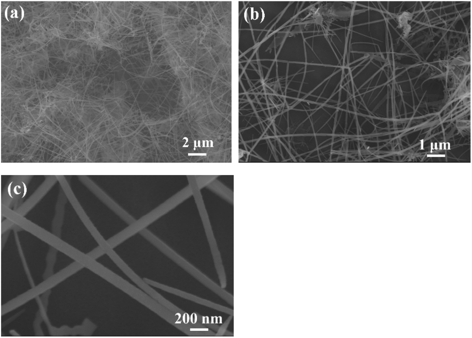 | ||
| Fig. 1 SEM images of CuNWs at different magnifications. | ||
The synthesized nanowires are scraped from the aluminum substrate in order to perform an XRD analysis (Fig. 2). Their diffraction peaks are divided into two groups, with the first group's signals appearing at 2θ = 38.5°, 44.7°, 65.1° and 78.3°, which correspond, respectively, to the (111), (200), (220) and (311) (JCPDF 46-1200) of the Al substrate's face-centered cubic (FCC) lattice. As for 2θ = 43.3°, 50.4° and 74.1°, they correspond, respectively, to the FCC Cu (111), (200) and (220) (JCPDF 04-0836). The EDS and XRD analyses confirm that the nanowires on the aluminum substrate are copper materials with a FCC structure.
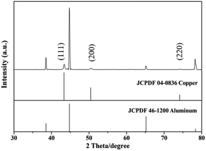 | ||
| Fig. 2 XRD pattern of CuNWs grown on rough Al foil. | ||
3.2 Microstructure analysis of CuNW growth
In Fig. 3, the SEM images show the changes to the CuNWs’ morphology at different reaction times during the growth process. At the reaction time of 30 and 60 min, it is observed that numerous agglomerations of Cu nanoparticles have appeared on aluminum foil, as can be seen in Fig. 3a and b. At these time points, some shorter CuNWs are already forming. After an hour, most of the Cu nanoparticles have been reduced on the aluminum surface, and at the same time, a greater number of longer CuNWs have grown on the substrate's surface. When the reaction time increases, the number of nucleation points and the length of the CuNWs will also increase. Additionally, the number of CuNWs will also increase sharply. As shown in Fig. 1a, thicker and longer CuNWs can be found across the entire surface of the aluminum substrate after 20 hours.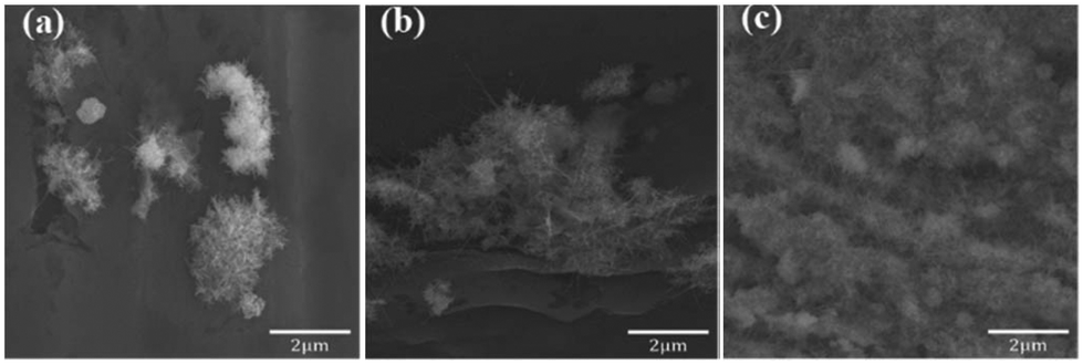 | ||
| Fig. 3 SEM images of one-dimensional CuNWs obtained to observe the morphology changes at the reaction time of (a) 30 min, (b) 60 min and (c) 90 min. | ||
In order to observe the growth direction and atomic arrangement of the CuNWs, a TEM analysis is carried out by using ultrasonication to disperse the CuNWs across a nickel grid. Fig. 4a and b show TEM bright-field images of the CuNWs at different magnification levels. Fig. 4c and d show the HRTEM image and the corresponding fast Fourier transform (FFT) analyses, respectively. The HRTEM image indicates that the lattice spacing d = 0.18 nm, which is consistent with the observations of the FCC Cu (200). An analysis confirms that the green diffraction spots are the Cu (200) and (020) (JCPDS 04-0836; Cu Fm![[3 with combining macron]](https://www.rsc.org/images/entities/char_0033_0304.gif) m), while the yellow diffraction spots are the Cu2O (200), (220) and (020) (JCPDS 05-0667; Cu2O Pnm). EDS line mapping is then performed to analyze the sample. As shown in Fig. 4e and f, it is clear that the CuNWs are coated by a thin Cu2O layer which forms the Cu@Cu2O cable-like one-dimensional nanomaterials. The SAED analysis reveals that the growth direction of the CuNWs is [100] and that their surfaces have oxidized to form native Cu2O. These findings were also observed in previous reports.5,9
m), while the yellow diffraction spots are the Cu2O (200), (220) and (020) (JCPDS 05-0667; Cu2O Pnm). EDS line mapping is then performed to analyze the sample. As shown in Fig. 4e and f, it is clear that the CuNWs are coated by a thin Cu2O layer which forms the Cu@Cu2O cable-like one-dimensional nanomaterials. The SAED analysis reveals that the growth direction of the CuNWs is [100] and that their surfaces have oxidized to form native Cu2O. These findings were also observed in previous reports.5,9
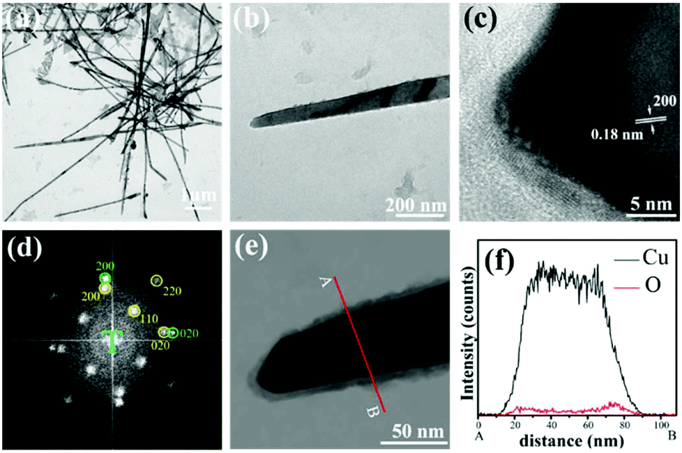 | ||
| Fig. 4 (a) and (b) TEM images of CuNWs with different magnifications; (c) an HRTEM image taken from the top of a CuNW in (b) showing the lattice fringes revealing the Cu (200) plane, separated by 0.18 nm; (d) electron diffraction patterns showing FCC Cu and Cu2O planes; (e) and (f) EDS line mapping of the CuNW showing a thin copper oxide layer coating on the CuNW. | ||
To understand the early growth characteristics of the CuNWs and the changes to the Al–Cu interface microstructure, a focused ion beam is used to slice the sample, obtained at the 30 min reaction time, into thin sections, after which a TEM analysis is performed. The specimen in Fig. 5a consists of CuNWs, Cu nanoparticles and Al foil, which is suitable for observing changes to the Al–Cu interface during the early reaction. The diameter of the CuNW at the center of the image is about 60 nm. EDS is used to observe the element distribution of the nanowires, nanoparticles, interface layer and Al substrate. The elemental composition and ratio at each position are shown in Fig. S2.† In the EDS mapping analysis, the colors green, red and blue indicate the distribution of the Cu, Al and O elements, respectively. Fig. 5c and d reveal the overlapping distribution of the Al and O elements across the Al–Cu interface and the periphery of the CuNWs and Cu nanoparticles.
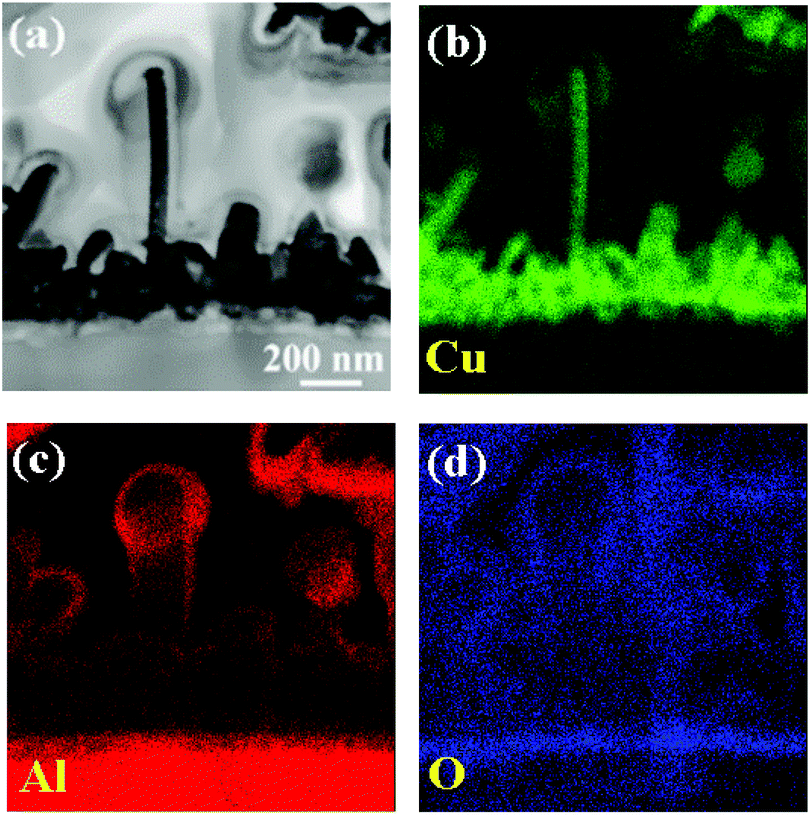 | ||
| Fig. 5 CuNWs’ (a) bright-field TEM image, (b) EDS mapping of copper, (c) EDS mapping of aluminum and (d) EDS mapping of oxygen at the 30 min reaction time point after the start of the reaction. | ||
As the reduction–oxidation reaction occurs on the solid–liquid interface, the Cu2+ ions on Al foil surface are reduced to Cu nanoparticles which aggregate on the substrate surface during the initial reaction. When the reaction continues, the number of Cu nanoparticles will gradually increase. The surfactant CTAC in the solution will suppress copper growth on certain crystal planes and cause it to grow in specific directions. This leads to the formation of one-dimensional CuNWs on the Cu nanoparticles’ aggregation points. Since the reaction occurs in an acidic environment with pH values of 2–3, the aluminum oxidizes into Al3+ ions and subsequently forms the AlOxHy interlayer between Al foil and Cu nanoparticles. This interface layer is formed from loose nanoparticles; hence electrons can still pass through and will not inhibit the reduction–oxidation reaction. Thin layers of Al(OH)x were detected through the use of an Auger microprobe or the performance of atom probe tomography, and the application of similar galvanic displacement methods to identify the deposition of copper films on Al.27,28 The concentration of Al3+ ions is higher near the Al surface as the reaction occurs on the solid–liquid phase interface. Therefore, the formation of AlOxHy is clearly shown in Fig. 5 and the Al element signals will not be detected when the CuNWs grow in length (Fig. 1). Furthermore, the Cu nanoparticles and the CuNWs’ surfaces are also covered by a layer of AlOxHy. According to the literature, one side of the CTAC bilayer binds to the Cu surface, while the other side interfaces with the aqueous medium.29,30 As a result, we predict that a high concentration of Al3+ ions will be adsorbed to the CTAC to form a bonding environment (![[triple bond, length as m-dash]](https://www.rsc.org/images/entities/char_e002.gif) N+–Cl−⋯Al3+), in which Al3+ ions will then transform into AlOxHy during the reaction or drying process. Similar chemical reaction designs have often been used to synthesize mesoporous alumina.31–34
N+–Cl−⋯Al3+), in which Al3+ ions will then transform into AlOxHy during the reaction or drying process. Similar chemical reaction designs have often been used to synthesize mesoporous alumina.31–34
Fig. 6 is a schematic representation illustrating the speculated growth process of the CuNWs based on the TEM and EDS analyses. During the initial reaction, the reduction–oxidation reaction occurs on the Al foil surface and Cu nanoparticles are produced. At the same time, the aluminum substrates will oxidize and form an AlOxHy thin film embedded between the Cu nanoparticles and Al metal. When the reaction continues and more Cu nanoparticles are produced, these nanoparticles will become the nucleation points for the CuNWs. Controlled by the surfactant that is added, the nanoparticles will grow in the [100] direction and form one-dimensional CuNWs. The continuing reaction is accompanied by an increase in the number and length of the CuNWs. As the reaction interface has a higher concentration of Al3+ ions, they will be adsorbed to the CTAC of the CuNWs’ root surfaces and be transformed into a layer of AlOxHy.
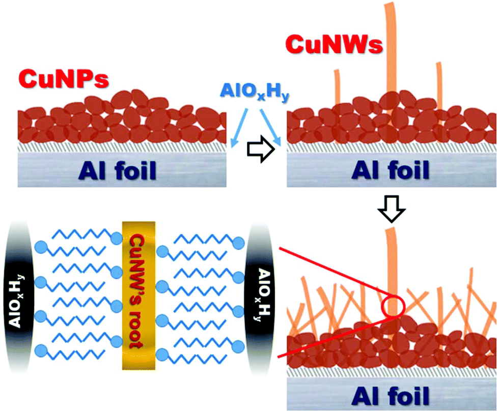 | ||
| Fig. 6 The schematic representation shows the growth of the CuNWs. The Cu2+ ions and Al metal undergo a reduction–oxidation reaction and Cu nanoparticles are produced. At the same time, a thin film of AlOxHy (section indicated by diagonal lines) forms on the interface. When the reaction continues, the CuNWs will gradually increase in length and quantity. At this point, the Al3+ ions will be adsorbed to the surface of the capping agent CTAC to form AlOxHy. | ||
In an Al–Cu galvanic displacement reaction, several factors, including the pH of the solution, temperature of the reaction, surface characteristics of the Al film and stoichiometry of the reactants, determine the morphology of the product. A series of experiments were conducted regarding control of the uniformity of product morphology. It is interesting to find that small changes to the pH value of the solution greatly affect the product's morphology. For the synthesis conditions of the CuNWs reported in this study, the pH of the solution is controlled at 2.2–2.3. Under the same synthesis conditions, changing the pH value of the reaction solution to 1.8–2.0 will lead to the formation of copper nanobelts, which are another unique one-dimensional Cu nanostructure (Fig. 7a and b). Moreover, when the pH of the reaction is increased to 2.5–3, one-dimensional Cu nanomaterials with a new morphology, rectangular nanotubes, are synthesized on a large-scale (Fig. 7c and d). A previous study revealed that the root segment of the rectangular copper nanotubes comprises solid-centered copper nanorods, which gradually form into hollow tube structures.5 It was found that the acidic environment may assist the dissolution of native oxide on Al foil so that the fresh Al metal surface can be exposed for galvanic reactions.9 Given the limited information available, an inference may only be made based on the product's morphology. A possible reason could be that metal dissolution in a more acidic environment (pH < 2) leads to the production of thinner nanobelts. When the pH is increased to >2.5, it then becomes possible to produce thicker rectangular Cu nanorods.
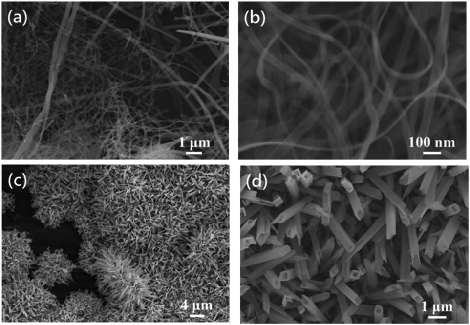 | ||
| Fig. 7 (a) and (b) When the reaction occurs at pH = 1.8–2.0, the product is Cu nanobelts. (c) and (d) When the reaction occurs at pH = 2.5–3.0, the product takes the form of rectangular nanotubes with roots formed from solid rectangular nanorods. | ||
3.3 Photocatalytic degradation
In the chemical industry, copper and copper oxides are considered to have good catalytic properties. In this experiment, MO is degraded in order to measure the magnitude of the photocatalytic performance.2–4 0.05 g of CuNWs are mixed with a 10 mL 30 ppm MO aqueous solution, exposed to AM 1.5G radiation for 0 to 24 min at room temperature and subsequently subjected to a UV-vis measurement analysis. The concentration of MO was monitored at 463 nm, which is the maximum absorbance wavelength of MO. (I0 − I)/I0 × 100% was used to calculate the degree of degradation, where I0 and I denote the absorption intensities at t = 0 and degradation time t, respectively. Fig. 8a shows a control experiment in which CuNWs are not added. After 24 min, the MO has essentially not degraded at all (degradation is merely 2%). When the CuNWs are added to the MO solution, the absorption peak intensity of the MO's maximum absorption band (463 nm) decreases when the time of exposure to light increases, indicating that the MO concentration is decreasing over time. After 12 min and 24 min, the reaction's degradation rate is 38% and 64%, respectively. When the MO is adsorbed to the nanostructure, it will be oxidized and decomposed. Fig. 8 shows that the CuNWs possess excellent photocatalytic properties for degrading organic dyes.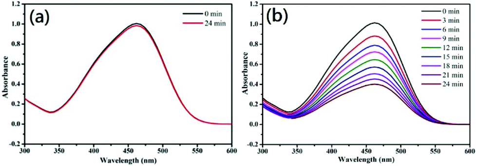 | ||
| Fig. 8 Methyl orange degradation efficiency test of CuNWs: (a) in control experiment with no CuNWs added, MO degrades by merely 2% after 24 min; (b) when CuNWs are added, the methyl orange degradation rate reaches 64% after 24 min. | ||
4. Conclusions
In this study, a galvanic displacement reaction is induced in an aqueous solution to synthesize one-dimensional CuNWs. An appropriate surfactant, CTAC, is added to a copper chloride solution to inhibit specific crystal plane growth. This provides a confining force that allows the copper, which has a cubic crystal structure, to undergo anisotropic growth. Acid catalysis is then carried out by adding nitric acid, and the artificially roughened aluminum foil is put into a water bath at a controlled temperature, so as to produce high yield, dimensionally uniform CuNWs. The growth characteristics of the CuNWs are tracked by observing them at various reaction time points, and it is revealed that an AlOxHy interlayer and Cu nanoparticles are formed when Al foil and Cu2+ ions undergo a reduction–oxidation reaction. CuNWs will start to grow on the Cu nanoparticle seeds in the [100] direction when the reaction time increases. The MO degradation experiments confirm that the CuNWs possess excellent photocatalytic properties. When the pH for the reaction is gradually increased from 1.8 to 3, the product's morphology gradually transforms into a structure consisting of nanobelts, then nanowires, and finally, rectangular nanorods. Although the galvanic reaction is considered a traditional technique, basic research is still needed to understand the fine variation in the microstructure that is associated with the reaction.Conflicts of interest
There are no conflicts to declare.Acknowledgements
The authors thank the Ministry of Science and Technology of Taiwan (MOST 106-2113 M-027-006) for financial support.Notes and references
- L. Xu, S. Sithambaram, Y. Zhang, C.-H. Chen, L. Jin, R. Joesten and S. L. Suib, Chem. Mater., 2009, 21, 1253–1259 CrossRef CAS.
- M. Yang and J. He, J. Colloid Interface Sci., 2011, 355, 15–22 CrossRef CAS PubMed.
- T. Kou, C. Jin, C. Zhang, J. Sun and Z. Zhang, RSC Adv., 2012, 2, 12636–12643 RSC.
- D. Jana and G. De, RSC Adv., 2012, 2, 9606–9613 RSC.
- Y.-H. Chang, Y.-T. Hsu, Y.-H. Tsai, Y.-R. Lai, T.-K. Huang and H.-T. Chiu, RSC Adv., 2015, 5, 108002–108006 RSC.
- A. Aziz, T. Zhang, Y.-H. Lin, F. Daneshvar, H.-J. Sue and M. E. Wellanda, Nanoscale, 2017, 9, 13104–13111 RSC.
- K. Liu, Y. Li, H. Zhang and Y. Liu, Appl. Surf. Sci., 2018, 439, 226–231 CrossRef CAS.
- R. Dang, L. Song, W. Dong, C. Li, X. Zhang, G. Wang and X. Chen, ACS Appl. Mater. Interfaces, 2014, 6, 622–629 CrossRef CAS.
- T.-K. Huang, T.-H. Cheng, M.-Y. Yen, W.-H. Hsiao, L.-S. Wang, F.-R. Chen, J.-J. Kai, C.-Y. Lee and H.-T. Chiu, Langmuir, 2007, 23, 5722–5726 CrossRef CAS.
- I.-C. Chang, T.-K. Huang, H.-K. Lin, Y.-F. Tzeng, C.-W. Peng, F.-M. Pan, C.-Y. Lee and H.-T. Chiu, ACS Appl. Mater. Interfaces, 2009, 1, 1375–1378 CrossRef CAS.
- C. F. Monson and A. T. Woolley, Nano Lett., 2003, 3, 359–363 CrossRef CAS.
- Y. Chang, M. L. Lye and H. C. Zeng, Langmuir, 2005, 21, 3746–3748 CrossRef CAS.
- C. Kim, W. Gu, M. Briceno, I. M. Robertson, H. Choi and K. Kim, Adv. Mater., 2008, 20, 1859–1863 CrossRef CAS.
- H. Choi and S.-H. Park, J. Am. Chem. Soc., 2004, 126, 6248–6249 CrossRef CAS.
- S. Xiao, P. Liu, W. Zhu, G. Li, D. Zhang and H. Li, Nano Lett., 2015, 15, 4853–4858 CrossRef CAS.
- X. Liu, Y. Sui, X. Yang, Y. Wei and B. Zou, ACS Appl. Mater. Interfaces, 2016, 8, 26886–26894 CrossRef CAS.
- N.-H. Tran, T.-H. Duong and H.-C. Kim, Sci. Rep., 2017, 7, 15093 CrossRef.
- H. Kim, S.-H. Choi, M. Kim, J.-U. Park, J. Bae and J. Park, Appl. Surf. Sci., 2017, 422, 731–737 CrossRef CAS.
- C. Hwang, J. An, B. D. Choi, K. Kim, S.-W. Jung, K.-J. Baeg, M.-G. Kim, K.-M. Ok and J. Hong, J. Mater. Chem. C, 2016, 4, 1441–1447 RSC.
- X. Wang, R. Wang, L. Shi and J. Sun, J. Mater. Chem. C, 2018, 6, 1048–1056 RSC.
- X. Wang, R. Wang, H. Zhai, X. Shen, T. Wang, L. Shi, R. Yu and J. Sun, ACS Appl. Mater. Interfaces, 2016, 8, 28831–28837 CrossRef CAS.
- H. Hwang, A. Kim, Z. Zhong, H.-C. Kwon, S. Jeong and J. Moon, Adv. Funct. Mater., 2016, 26, 6545–6554 CrossRef CAS.
- S. Ding, J. Jiu, Y. Gao, Y. Tian, T. Araki, T. Sugahara, S. Nagao, M. Nogi, H. Koga, K. Suganuma and H. Uchida, ACS Appl. Mater. Interfaces, 2016, 8, 6190–6199 CrossRef CAS.
- L.-L. Lu, J. Ge, J.-N. Yang, S.-M. Chen, H.-B. Yao, F. Zhou and S.-H. Yu, Nano Lett., 2016, 16, 4431–4437 CrossRef CAS.
- Z. Yin, S. Cho, D.-J. You, Y.-K. Ahn, J. Yoo and Y. S. Kim, Nano Res., 2018, 11, 769–779 CrossRef CAS.
- T.-K. Huang, K.-W. Lin, S.-P. Tung, T.-M. Cheng, I.-C. Chang, Y.-Z. Hsieh, C.-Y. Lee and H.-T. Chiu, J. Electroanal. Chem., 2009, 636, 123–127 CrossRef CAS.
- J. H. Ai, S. P. Liu, N. A. Widharta, S. Adhikari, J. W. Anderegg and K. R. Hebert, J. Phys. Chem. C, 2011, 115, 22354–22359 CrossRef CAS.
- Y. Zhang, J. Ai, A. C. Hillier and K. R. Hebert, Langmuir, 2012, 28, 1673–1677 CrossRef CAS.
- B. Nikoobakht and M. A. El-Sayed, Langmuir, 2001, 17, 6368–6374 CrossRef CAS.
- J. Gao, C. M. Bender and C. J. Murphy, Langmuir, 2003, 19, 9065–9070 CrossRef CAS.
- J. H. Kim, K. Y. Jung and K. Y. Park, J. Ceram. Soc. Jpn., 2010, 118, 805–809 CrossRef CAS.
- R. V. Pai, K. T. Pillai, S. Pathak, S. K. Mukerjee, V. V. Vinogradov, A. V. Agafonov, A. V. Vinogradov and S. K. Aggarwal, J. Sol-Gel Sci. Technol., 2012, 61, 192–196 CrossRef CAS.
- W. Deng, M. W. Toepke and B. H. Shanks, Adv. Funct. Mater., 2003, 13, 61–65 CrossRef CAS.
- S. Cabrera, J. E. Haskouri, J. Alamo, A. Beltrán, D. Beltrán, S. Mendioroz, M. D. Marcos and P. Amorós, Adv. Mater., 1999, 11, 379–381 CrossRef CAS.
Footnote |
| † Electronic supplementary information (ESI) available. See DOI: 10.1039/c8qi00826d |
| This journal is © the Partner Organisations 2019 |