
Realizing a stable high thermoelectric zT ∼ 2 over a broad temperature range in Ge1−x−yGaxSbyTe via band engineering and hybrid flash-SPS processing†
Bhuvanesh
Srinivasan
 *ab,
Alain
Gellé
c,
Francesco
Gucci
b,
Catherine
Boussard-Pledel
a,
Bruno
Fontaine
a,
Régis
Gautier
a,
Jean-François
Halet
*a,
Michael J.
Reece
b and
Bruno
Bureau
a
*ab,
Alain
Gellé
c,
Francesco
Gucci
b,
Catherine
Boussard-Pledel
a,
Bruno
Fontaine
a,
Régis
Gautier
a,
Jean-François
Halet
*a,
Michael J.
Reece
b and
Bruno
Bureau
a
aUniv. Rennes, Ecole Nationale Supérieure de Chimie de Rennes, CNRS, ISCR – UMR 6226, F-35000 Rennes, France. E-mail: bhuvanesh.srinivasan@univ-rennes1.fr; jean-francois.halet@univ-rennes1.fr
bSchool of Engineering and Materials Science, Queen Mary University of London, London E1 4NS, UK
cUniv. Rennes, CNRS, IPR – UMR 6251, F-35000 Rennes, France
First published on 3rd October 2018
Abstract
We report a remarkably high and stable thermoelectric figure of merit zT close to 2 by manipulating the electronic bands in Ga–Sb codoped GeTe, which has been processed by hybrid flash-spark plasma sintering. According to the experimental results and first-principles calculations, the vast enhancement achieved in the thermopower due to codoping of Ga (2 mol%) and Sb (8 mol%) in GeTe is attributed to a concoction of reasons: (i) suppression of hole concentration; (ii) improved band convergence by decreasing the energy separation between the two valence band maxima to 0.026 eV; (iii) Ga predominantly contributing to the top of the valence band in Ga–Sb codoped GeTe, despite the Ga-induced resonance state not being located at a favorable position near the Fermi level; (iv) active participation of several bands increasing the hole carrier effective mass; (v) facilitating band degeneracy by reducing the R3m → Fm![[3 with combining macron]](https://www.rsc.org/images/entities/char_0033_0304.gif) m structural transition temperature from 700 K to 580 K. The synergy between these complementary and beneficial effects, in addition to the reduced thermal conductivity, enabled the flash sintered Ge0.90Ga0.02Sb0.08Te composition to not only exhibit a peak of zT of ∼1.95 at 723 K, but also to maintain/stabilize its high performance over a broad temperature range (600–775 K), thus making it a serious candidate for mid-temperature range energy harvesting devices.
m structural transition temperature from 700 K to 580 K. The synergy between these complementary and beneficial effects, in addition to the reduced thermal conductivity, enabled the flash sintered Ge0.90Ga0.02Sb0.08Te composition to not only exhibit a peak of zT of ∼1.95 at 723 K, but also to maintain/stabilize its high performance over a broad temperature range (600–775 K), thus making it a serious candidate for mid-temperature range energy harvesting devices.
1. Introduction
Within the realms of exploring alternative means to power the planet, the requirement of generating and storing energy sustainably represents one of the critical challenges across the boundaries of science and technology in the 21st century. In this regard, thermoelectric (TE) materials and devices have drawn increasing interest and attention due to their potential to reversibly convert waste heat into fruitful electricity. A TE material's efficiency is generally quantified by the dimensionless figure of merit defined as zT = S2σT/κtotal where S, σ, T and κtotal are the Seebeck coefficient, electrical conductivity, temperature and total thermal conductivity (sum of the electronic part, κe, and the lattice part, κlatt), respectively. The main paradigm to achieve high zT in materials is to enhance their power factor (S2σ) and/or reduce their thermal transport properties (κtotal). Most of the TE research activities are aimed at reducing κlatt to enhance zT by phonon scattering due to nanostructuring,1–3 intrinsic bond anharmonicity,4–6 rattling impurities,7etc. However, S and σ are highly intertwined and present a greater challenge in enhancing the power factor, paramount for better energy conversion efficiency. Advances in recent times have shown that the concept of ‘band structure engineering’, which includes convergence of electronic band valleys,8,9 quantum confinement of electron charge carriers,10 electron filtering,11 inducing resonant levels by impurities near the Fermi level,12 nestification,13 dimensionality reduction,14 deformation potential coefficient,15 and effective mass,16 is effective in decoupling S and σ to a certain extent. Even the idea of semiconducting chalcogenide glasses (based on the phonon-glass electron-crystal approach) as potential thermoelectric materials has been tried with varying degrees of success.17–20Though the concept of band engineering is extensively applied to various p- and n-type materials like SnTe,21–25 PbTe,26–28 half-Heuser29 and Mg2Si,30 it is applied relatively less on GeTe-based materials. Some of the strategies for GeTe-based materials to enhance the power factor and/or to suppress κlatt have been adopted on compositions such as GeTe–AgSbTe2 (TAGS),31 GeTe–LiSbTe2,32 GeTe–AgInTe2,33 GeTe–AgSbSe2,34 (GeTe)nSb2Te3,35 Ge1−xPbxTe,36 Ge1−xBixTe,37 (Bi2Te3)nGe1−xPbxTe,38 Ge1−xInxTe,39 GeTe1−xSe,40 Ge1−xSbxTe,41,42 Ge1−xAgxTe,43 Ge1−xMnxTe,44,45 Ge1−x−ySnxPbyTe,46 Ge1−xSbxTe1−ySey,47 GeTe–GeSe–GeS,48 Ge1−x−yBixSbyTe,49 Ge1−x−yBixInyTe25 and more recently Ge0.9−yPb0.1BiyTe.50 The crystal structure of GeTe-based compounds undergoes a second-order ferroelectric structural transition from rhombohedral symmetry (low temperature phase) to cubic symmetry (high temperature phase) at around 700 K.51 Motivated by the results of Wu et al. on Ge1−xInxTe,39 showing that the introduction of resonant levels in the vicinity of the Fermi level due to indium doping leads to a reasonably high zT in GeTe (zT ∼1.3 at 630 K), we here have tried to explore the effect of another group 13 element, namely Ga, on the TE performance of GeTe. From the latest work on Ge1−x−yBixSbyTe,49 it was also established that 8–10 mol% Sb doping in GeTe helped to improve the band degeneracy by pushing the system towards the cubic structure (c-GeTe). Hence aiming at bringing in synergistic band effects, we investigated the effect of codoping of Ga and Sb on the structural, electronic and thermoelectric properties of GeTe. As group 13 elements and Sb have distinctive roles, we expect codoping of Ga and Sb in GeTe to result in a synergistic band effect, i.e., the cumulative effect of resonant states induced by Ga and band degeneracy caused by Sb, which ultimately should increase the thermopower of the material.
Compounds with the nominal compositions of Ge1−xGaxTe (x = 0.00–0.10) were synthesized by vacuum-sealed tube melt processing, followed by consolidation by Spark Plasma Sintering (SPS). The optimum content of resonant states was achieved when 2 mol% Ga was substituted for Ge in GeTe. Indeed, this substitution marginally improved the thermoelectric performance (zT ∼ 1.1 at 720 K) when compared to pristine GeTe (zT ∼ 0.95 at 720 K). Furthermore, when 8–10 mol% Sb was codoped to Ge0.98Ga0.02Te, we successfully realized the co-adjuvant synergistic band effects in GeTe. Thus, the Ge0.88Ga0.02Sb0.10Te composition with a high thermopower and ultra-low κtotal manifested a maximum zT ∼ 1.75 at 725 K, which was 80% higher than that of pristine GeTe. With the state-of-the art ‘hybrid flash-SPS’ processing,52,53 this zT value was further improved to ∼2 at 725 K (more than 100% improvement when compared to undoped GeTe). Interestingly, this high value of zT is notably maintained over a broad temperature range (600–775 K). The results obtained for Ge1−xGaxTe (x = 0.00–0.10) are first discussed, followed by Ge1−x−yGaxSbyTe (x = 0.02; y = 0.08–0.10). Note that all results are presented together in the same figures and tables for a better comparison. Owing to their meager TE properties, the results of Ge0.90Ga0.10Te are given in the ESI.†
2. Materials & methods
Reagents
Ge (Umicore, 99.999%), Sb (Alfa Aesar, 99.999%), Ga (Alfa Aesar, 99.999%) and Te (JGI, 99.999%) were used for synthesis without any further purification.Synthesis
Samples of Ge1−xGaxTe (x = 0.00–0.07) and Ge1−x−yGaxSbyTe (x = 0.02; y = 0.08, 0.10) were synthesized using vacuum-sealed tube melt processing. Appropriate stoichiometric amounts of the starting elements of Ge, Ag and Te were introduced into a fused silica tube that had previously been cleaned with hydrofluoric (HF) acid and distilled water and dried under vacuum. The ampoules were sealed under a vacuum of 10−6 Torr, then placed in a rocking furnace and slowly heated up to 950 °C over a period of 12 hours, and then held at that temperature for 12 hours and slowly cooled down to room temperature. The obtained ingots were crushed and milled. The powders were then consolidated by SPS (FCT Systeme GmbH) at 723 K (heating rate ∼80 °C min−1) for 5 min (holding time) under an axial pressure of 85 MPa. The sample with better TE properties was also consolidated by ‘hybrid’ flash-SPS processing, where the powders were sintered at 893 K and a heating rate of ∼10![[thin space (1/6-em)]](https://www.rsc.org/images/entities/char_2009.gif) 000 °C min−1 (heated from 293–893 K in 3 seconds) under an axial pressure of 55 MPa. More information regarding this processing technique is provided in the ESI.† The schematics of the experimental set-up and the current flow paths for SPS (graphite punches and die), flash-SPS (graphite punches and no die) and hybrid flash-SPS (graphite punches and a thin walled stainless steel die) configurations are compared and explained in the ESI (Fig. S1 and Table S1†). Highly dense disk-shaped pellets were obtained with theoretical densities of 100% for SPS and ∼98% for hybrid flash-SPS. The obtained ingots and sintered discs were cut and polished to the required shapes and dimensions for various thermoelectric measurements.
000 °C min−1 (heated from 293–893 K in 3 seconds) under an axial pressure of 55 MPa. More information regarding this processing technique is provided in the ESI.† The schematics of the experimental set-up and the current flow paths for SPS (graphite punches and die), flash-SPS (graphite punches and no die) and hybrid flash-SPS (graphite punches and a thin walled stainless steel die) configurations are compared and explained in the ESI (Fig. S1 and Table S1†). Highly dense disk-shaped pellets were obtained with theoretical densities of 100% for SPS and ∼98% for hybrid flash-SPS. The obtained ingots and sintered discs were cut and polished to the required shapes and dimensions for various thermoelectric measurements.
Powder X-ray diffraction
X-ray diffraction (XRD) patterns were recorded at room temperature in the 2θ range of 15–120° with a step size of 0.026° and a scan time per step of 400 s using a PANalytical X'Pert Pro diffractometer (Cu K-L2,3 radiation, λ = 1.5418 Å, PIXcel 1D detector).Hall measurements
Hall measurements were carried out at room temperature using a home-made four-point probe setup (van der Pauw method), where a fixed magnetic field of 0.112 T and a dc current of 15 mA were applied. The measurements were made on square-shaped samples of dimensions ∼5 × 5 × 2 mm3. The carrier concentration (n) and mobility (μ) were computed using the following equations,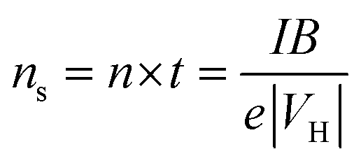 | (1) |
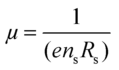 | (2) |
Electrical and thermal transport
For each sample, the electrical resistivity and Seebeck coefficient were measured simultaneously from room temperature to 723 K using a commercial instrument (LSR-3, Linseis Inc.), under a He atmosphere. The measurements were made on rectangular samples of dimensions ∼10 × 2 × 2 mm3.The thermal diffusivity, D, was measured from room temperature to 723 K using the laser flash diffusivity method with a Netzsch LFA-457 instrument. Disc-shaped samples of 10 mm diameter and ∼2 mm thickness were used for the measurements. The temperature dependent heat capacity, Cp, was derived using the Dulong–Petit relation as in eqn (3),
| Cp = 3R/M | (3) |
The total thermal conductivity κtotal was calculated using eqn (4),
| κtotal = DCpρ | (4) |
To better understand the thermal transport properties, the contributions from electronic and lattice parts were calculated. The lattice thermal conductivity (κlatt) was estimated from κtotal by subtracting the electronic contribution (κe) via the Wiedemann–Franz law, as in eqn (5),
| κe = LσT | (5) |
 | (6) |
The uncertainty in the results for the values of electrical and thermal transport properties was ∼5% and ∼7%, respectively and for the overall zT it was ∼12%. Error bars are not shown in the figures to increase readability.
Computational procedures
Density Functional Theory (DFT) calculations were performed to understand the effect of doping on the electronic states. We used the projector-augmented-wave (PAW) approach56 implemented in the Vienna ab initio simulation package (VASP).57 Calculations were performed using generalized gradient approximation (GGA) for the exchange–correlation term parametrized by Perdew et al.58 Spin orbit coupling was also included in the computations.As we were interested in the high temperature behavior of doped GeTe, calculations were performed on the cubic structural models. Impurities were substituted to the Ge atom in a 4 × 4 × 4 super-cell. Considering the previous study by Hoang et al.59 on the impurity clustering in GeTe, we adopted a cluster of one Ga atom surrounded by 6 Sb atoms (second neighbors) for the Ga–Sb codoped GeTe composition (Sb6GaGe57Te64). In order to understand the relative effect of both atoms, the calculations were also performed for GaGe63Te64 and Sb6Ge58Te64 models. In all the three cases, the positions were fully relaxed. For the irreducible cell, the Brillouin-zone integration was performed using a 25 × 25 × 25 Monkhorst–Pack k-mesh. For the super cell, we used a 3 × 3 × 3 k-mesh for the atom relaxation and a 7 × 7 × 7 k-mesh for the DOS calculations.
The carrier effective mass (m*) was derived for each sample using a single parabolic band model60,61 and the measured room temperature Seebeck coefficient (S) and carrier concentration (n). The chemical potential (μ) was estimated using eqn (7) with λ = 0 (acoustic-phonon scattering), where Fj(μ) is the Fermi integral given by eqn (8). The hole effective mass can then be determined from eqn (9).
 | (7) |
 | (8) |
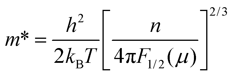 | (9) |
3. Results & discussion
Sharp reflections from powder XRD indicated the good crystalline nature of all of the synthesized ingots (Fig. 1). All of the main reflections could be indexed to a rhombohedral GeTe phase (PDF#47-1079, R3m space group). The rhombohedral phase was further confirmed by the presence of double reflections [(024) and (220)] in the range of 2θ values between 41° and 44° in Ge1−xGaxTe. Minor reflections of Ge impurities could be detected in some samples, which could be due to intrinsic Ge vacancies, as GeTe always prefers to have a Te-rich composition, in agreement with the previous experiments.43,49,62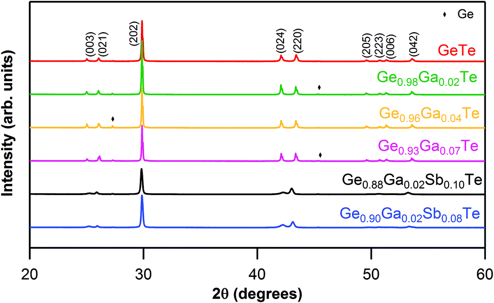 | ||
| Fig. 1 Powder XRD patterns for Ge1−xGaxTe (x = 0 to 0.07) and Ge1−x−yGaxSbyTe (x = 0.02; y = 0.08, 0.10) samples. | ||
Holes were the major charge carriers (p-type), as the Hall voltage was positive in these samples. The results from Hall measurements are presented in Table 1. The carrier concentration value at room temperature decreased with increasing Ga content. In pristine GeTe, the Ge vacancy has a very low formation energy and is the most easily formed intrinsic defect.62,63 The addition of Ga to GeTe can suppress these Ge vacancies, thereby leading to a reduction in the density of charge carriers. In most cases, the carrier mobility, μ, will increase with the decreasing charge carrier density. However, the mobility values in Ge1−xGaxTe had a contrasting effect, where they consistently reduced with increasing Ga content. This reduction in mobility with Ga content can be due to the increased density of ionized impurities and/or alloy scattering. Such mobility reductions are commonly observed in materials with group 13 dopants.12,39
| Sample | Carrier concentration, n (cm−3) | Mobility, μ (cm2 V−1 s−1) | Effective mass, m* |
|---|---|---|---|
| GeTe | 9.08 × 10²⁰ | 57.01 | 1.30me |
| Ge0.98Ga0.02Te | 8.73 × 10²⁰ | 51.76 | 1.72me |
| Ge0.96Ga0.04Te | 7.85 × 10²⁰ | 43.72 | 1.64me |
| Ge0.93Ga0.07Te | 6.35 × 10²⁰ | 32.04 | 1.65me |
| Ge0.88Ga0.02Sb0.10Te | 1.83 × 10²⁰ | 29.65 | 1.97me |
| Ge0.90Ga0.02Sb0.08Te | 3.96 × 10²⁰ | 29.82 | 2.38me |
| Ge0.90Ga0.02Sb0.08Te by hybrid flash-SPS | 2.13 × 10²⁰ | 35.81 | 2.03me |
The electrical conductivity of all of the samples decreased with temperature (Fig. 2a), which is the archetypal behavior of degenerate semiconductors. The Ga-doping systematically increased the electrical resistance, a reflection of the cumulative effect of deflation in both the charge carrier density and mobility with Ga content. The Seebeck coefficient, S, was positive for all the composition over the entire temperature range (Fig. 2b). This indicated p-type charge carriers, consistent with the Hall measurement results. With the increasing Ga content, there was a notable improvement in S values both at room temperature and at higher temperature for Ge1−xGaxTe samples. This modest improvement in S values can be attributed to the suppression of the carrier concentration by Ga doping. The temperature dependence of the power factors (S2σ) is shown in Fig. 2c for Ge1−xGaxTe samples. Compared to pristine GeTe, there was a marginal but significant improvement in the power factor for the 2 mol% Ga doped sample, which exhibited a maximum power factor of ∼4.1 × 10⁻³ W m−1 K−2 at 720 K. The advantage of an improved power factor in GeTe by 2 mol% Ga doping was maintained across the measured temperatures. The power factors of other Ge1−xGaxTe samples for x > 0.02 were lower than the undoped sample. Hence in the Ge1−xGaxTe system, the optimized value of x = 0.02 provided the needed proper trade-off between the electrical transport properties.
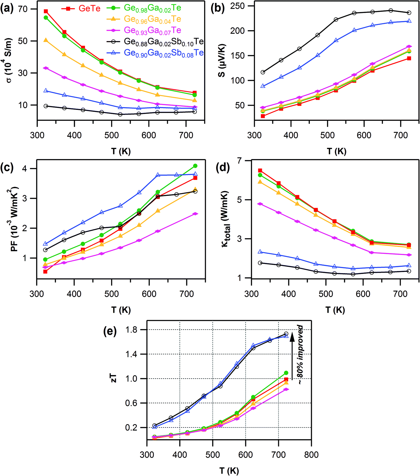 | ||
| Fig. 2 Temperature-dependent (a) electrical conductivity (σ), (b) Seebeck coefficient (S), (c) power factor (PF = S2σ), (d) total thermal conductivity (κtotal), and (e) figure of merit (zT) for Ge1−xGaxTe (x = 0.00–0.07) and Ge1−x−yGaxSbyTe (y = 0.02; z = 0.08, 0.10) samples. | ||
The total thermal conductivity, κtotal (Fig. 2d), monotonically decreased with Ga content in Ge1−xGaxTe samples. The contributions from the electronic (κe) and lattice (κlatt) parts are presented in the ESI (Fig. S5†). The temperature dependent Lorenz number, L, obtained by fitting their respective Seebeck coefficients for the samples of Ge1−xGaxTe was in the range of 2.3 × 10⁻⁸ to 1.8 × 10⁻⁸ WΩK−2 and lower than the metallic limit of 2.45 × 10⁻⁸ WΩK−2 (ESI, Fig. S4†). In the case of Ge1−xGaxTe, the majority of the thermal contribution came from κe, which conspicuously decreased with Ga content. κlatt of the Ga-doped samples was larger than that of the pristine GeTe, and this can arise when the estimation of the L value cannot properly account for the electronic contribution to the thermal conductivity, as similarly observed for previously reported PbTe and SnTe based materials.64,65
The maximum thermoelectric figure of merit, zT (Fig. 2e), achieved within the Ge1−xGaxTe (x = 0.00 to 0.10) series was ∼1.1 at 720 K for Ge0.98Ga0.02Te, which was marginally higher than that of pristine GeTe (zT ∼0.95 at 720 K). The zT values systematically decreased for the value of x > 0.02 in the Ge1−xGaxTe system. The heavily Ga-doped sample (x = 0.10) exhibited the lowest zT (ESI, Fig. S6†), due to its high electrical resistivity arising from severe deflation of the carrier concentration and mobility. Based on this evidence, it was concluded that 2 mol% Ga doping was optimum to achieve a better trade-off between S, σ and κtotal in the Ge1−xGaxTe (x = 0.00 to 0.10) series. The first-principles (density functional theory (DFT) type) calculations reported later in this paper suggest that resonant states are induced.
It has been reported that 8–10 mol% Sb doping in GeTe significantly helped to achieve band degeneracy.49 To further improve the thermoelectric performance of Ge0.98Ga0.02Te, Sb was codoped to it to form the Ge1−x−yGaxSbyTe (x = 0.02; y = 0.08, 0.10) series, with an objective to bring in synergistic band effects that would help to improve the TE performance.
As observed from the XRD patterns (Fig. 1), the double reflections [(024) and (220)] in the range of 2θ values between 41° and 44°, characteristic of the rhombohedral phase, got closer and almost merged when Sb was codoped into Ge1−xGaxTe. As the atomic radii of Ga (1.36 Å) and Sb (1.33 Å) are larger compared to that of Ge (1.25 Å), the codoping of Ga–Sb has relaxed the rhombohedral structure of GeTe and has pushed the system towards the cubic structure. In other words, Ga–Sb codoping has promoted a faster structural transition (R3m → Fmm) in GeTe. This was proven by the DSC data (ESI, Fig. S2†), where the structural transition temperature was conspicuously reduced from ∼630 K for Ge0.98Ga0.02Te to ∼580 K for Ge0.88Ga0.02Sb0.10Te. Considering that the transition temperature for pristine GeTe is ∼700 K, the codoping of Ga and Sb has tremendously reduced the phase transition temperature and has increased the cubic nature of the sample. From the band structure features of rhombohedral (r) and cubic (c) GeTe, it was shown that the latter has a larger total band degeneracy.66
Because of the combined actions of Ga and Sb at the Ge site in GeTe, an effective suppression of the intrinsic Ge vacancies could take place, which was reflected in the major reduction of the carrier concentration in the codoped samples (Table 1). Obviously, this contributed to the decline in σ for Ga–Sb codoped samples (Fig. 2a). But this was well compensated by the large increase in the Seebeck coefficient (Fig. 2b). The Ga–Sb codoped sample of composition Ge0.88Ga0.02Sb0.10Te exhibited a high thermopower of ∼120 μV K−1 at room temperature and a maximum of ∼240 μV K−1 at higher temperatures, an improvement by 70% when compared to pristine GeTe. It is also key to note that the S values of the codoped samples increased steeply until 550 K and almost became constant after that. Such a trend once again was a clear indication of the second order structural transition (R3m → Fmm).
The increased electrical resistivity, due to the lowering of carrier density and mobility, has immensely reduced the electronic contribution to thermal transport in the Ga–Sb codoped samples (ESI, Fig. S5a†). This has led to an ultra-low κtotal (<1.3 W m−1 K−1 at T > 500 K) in the Ge1−x−yGaxSbyTe samples (Fig. 2d). At room temperature, the Ge0.88Ga0.02Sb0.10Te sample exhibited a κtotal ∼1.75 W m−1 K−1, which accounted for a reduction by 270% when compared to pristine GeTe (κtotal ∼6.5 W m−1 K−1 at room temperature).
The combined beneficial effects of improved thermopower and reduced thermal transport, achieved by Ga–Sb codoping of GeTe, have strikingly enhanced the thermoelectric figure of merit (Fig. 2e). The Ga–Sb codoped GeTe samples (both Ge0.88Ga0.02Sb0.10Te and Ge0.90Ga0.02Sb0.08Te compositions) manifested a high zT ∼1.75 at 730 K, an improvement by 80% compared to undoped GeTe, and it is notably one of the highest reported among the GeTe-based materials.
To have a more cogent understanding on the effects of doping in GeTe, DFT calculations were performed (see the ESI† for the computational details). As we are interested in the high temperature domain for thermoelectric applications, these DFT calculations were carried out on 4 × 4 × 4 supercells derived from the cubic structural arrangement of GeTe. The electronic densities of states (DOS) computed for the cubic models of GeTe and Ge0.98Ga0.02Te are presented and compared in Fig. 3a. As expected, the presence of some amounts of Ga in GeTe shifted the Fermi level towards the valence band. The DOS was clearly modified near the top of the valence band with respect to that of GeTe, distinctly indicated by the presence of a sharp hump near the Fermi level (EF). This firmly establishes that Ga doping induces resonant states or deep defect states near EF in the electronic band structure of GeTe. According to Mott's relationship,67 the modified DOS obtained by resonant levels may contribute to an improvement in the Seebeck coefficient. This explains the marginal raise in thermopower for Ge1−xGaxTe at high temperatures (cubic phase). However, the power factor and zT were improved only for the Ge0.98Ga0.02Te composition, while they were reduced for higher dopant content of Ga in Ge1−xGaxTe (x > 0.02). This happens because the distortion of DOS (resonant states) hinders the electrical conductivity (owing to reduced mobility). At higher dopant levels of Ga (>2 mol%), the DOS of the samples are modified heavily, which was reflected in their poor TE performance due to their decreased σ and μ values. Hence, the 2 mol% Ga doping in GeTe produced the optimum distortion of the DOS to notably increase the thermopower without compromising much the electrical conductivity in Ge1−xGaxTe. It seems that the Ga-induced resonance level becomes more prominent only at the high temperature cubic phase, as there was not much significant change in the room temperature value of the Seebeck coefficient when 2 mol% Ga was doped to GeTe.
 | ||
| Fig. 3 Calculated DOS for (a) GaGe63Te64 (Ge0.98Ga0.02Te), (b) Sb6Ge58Te64 (Sb0.09Ge0.91Te) and (c) GaSb6Ge57Te64 (Ga0.02Sb0.09Ge0.89Te) models (derived from the high temperature cubic GeTe phase). The DOS of each model is compared with that of the pristine cubic phase Ge64Te64 (GeTe). The Fermi level (EF) of pristine GeTe is set arbitrarily at 0 eV. Green and red curves represent Sb and Ga projections. The dashed line represents the shifted Fermi level for the doped compositions. Additional Gaussian smearing of 25 meV was applied and the Ga projected DOS was magnified for a better readability of the curves. | ||
To simulate 8–10 mol% Sb doping in GeTe, six Sb atoms were substituted for Ge in GeTe leading to the Sb6Ge58Te64 (Sb0.09Ge0.91Te) composition. Among the different possible Sb distributions, that with Sb aggregation (i.e., Sb atoms close to each other) was considered to be the most thermodynamically stable.36 Computed DOS for this Sb doped (Sb6Ge58Te64 = Sb0.09Ge0.91Te) composition and for the Ga–Sb codoped (GaSb6Ge57Te64 = Ga0.02Sb0.09Ge0.89Te) GeTe (cubic) compositions are presented in Fig. 3b and c, respectively. Substituting in a 1/10 ratio of divalent Ge with Sb (Sb single doping) or with Ga + Sb (codoping of Ga and Sb) suppresses the hole concentration and, assuming a rigid band model, shifts the Fermi level (EF) upwards, i.e., towards the conduction band (Fig. 3b and c). We would like to mention that these statements must be considered with caution, as the theoretical calculations were performed based on a stoichiometric GeTe, where there is no Ge vacancy. But as found experimentally, GeTe always prefers to be in Te-rich composition and hence there exist some Ge vacancies. The p-type charge carriers still dominate the transport in Ga–Sb codoped GeTe, as observed from the Hall measurement results (Table 1). The significant reduction in the carrier density indicates that the DOS at the Fermi-level will decrease and the EF should be close to the gap for Ga–Sb codoped GeTe. According to the Boltzmann equation, such a scenario will obviously lead to an improved Seebeck coefficient, consistent with our experimental findings. Ga–Sb codoping adds donor states just below the conduction band of GeTe. Interestingly, we still found some Ga-induced resonant states in the top of the valence band when Sb was codoped to the Ge–Ga–Te system, but unlike the single doped Ge1−xGaxTe, the resonant state was not near EF in the Ga–Sb codoped system (Fig. 3c).
The electronic band structures of the undoped, doped and codoped compositions were also computed and analyzed, hoping to provide useful insight on how the valence band structure is modified upon doping. They are plotted in Fig. 4 along some high symmetry lines of the cubic Brillouin zone (BZ). From the electronic band structure of GeTe (Fig. 4b and c), the direct band gap was calculated to be 225 meV at the Γ point, which is in agreement with the literature.49,66 GeTe exhibits a second maximum of the valence band in the Γ → K (Σ) direction. The energy difference between light and heavy hole valence bands (ΔELΣ) for undoped cubic Ge64Te64 was found to be 64 meV, consistent with a recent report.66 This ΔELΣ value for c-GeTe is much lower when compared to that of the low temperature r-GeTe (ΔELΣ = 150 meV).66 This is advantageous and is in agreement with the fact that the temperature increases the band convergence in GeTe.38 As mentioned before, the ferroelectric structural transition was more favored with the codoping of Ga–Sb, since the transition temperature was reduced (ESI, Fig. S2†). This structural strain relaxation from rhombohedral low symmetry (R3m) to cubic high symmetry (Fmm) will increase the electronic band valley degeneracy, a key factor for enhancing the Seebeck coefficient. Thus, codoping of Ga–Sb to GeTe promotes the band valley convergence.
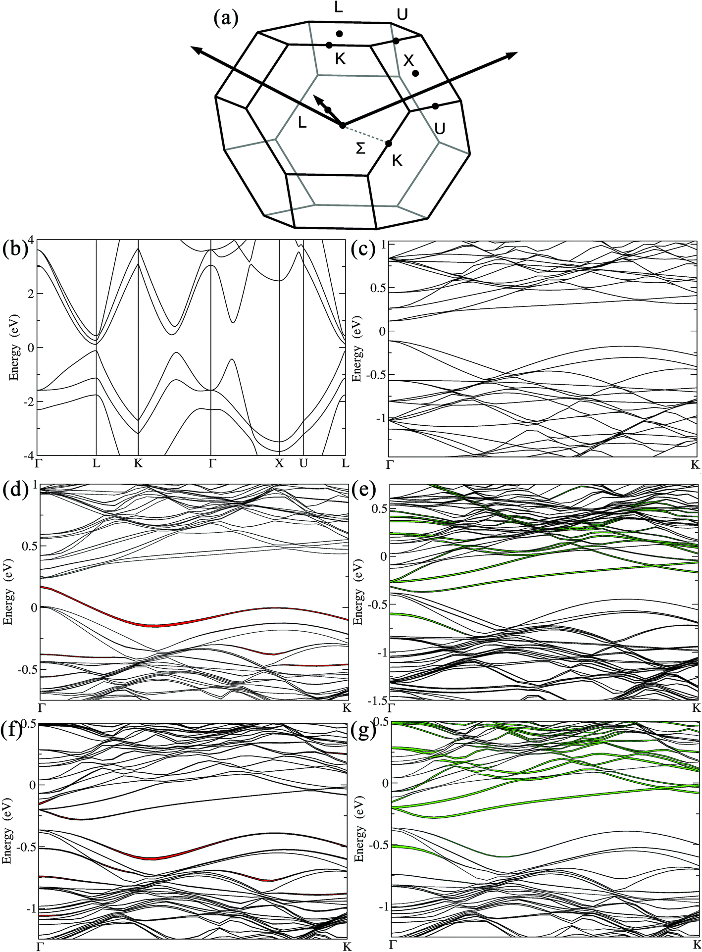 | ||
| Fig. 4 (a) Brillouin zone of c-GeTe. The band structures for (b) c-GeTe with a primitive unit cell; (c) c-Ge64Te64 using a 4 × 4 × 4 supercell showing band folding in the Γ → K (Σ) direction. (d) GaGe63Te64 (Ge0.98Ga0.02Te); (e) Sb6Ge58Te64 (Sb0.09Ge0.91Te); (f) GaSb6Ge57Te64 (Ga0.02Sb0.09Ge0.89Te) highlighting Ga projections and (g) GaSb6Ge57Te64 (Ga0.02Sb0.09Ge0.89Te) highlighting Sb projections. The line thickness is proportional to the projection of the wave function on the Ga (in red) and Sb (in green) orbitals. | ||
When 2 mol% Ga was added to GeTe, i.e., for (Ge0.98Ga0.02Te), the new impurity band arising from Ga states reduced the gap at the Γ point to 66 meV (Fig. 4d). The impurity states were located at the top of the valence band and extended somewhat within the gap. For 8–10 mol% Sb doping in GeTe, i.e. Sb6Ge58Te64 (Sb0.09Ge0.91Te), the Sb states were located at the bottom of the conduction band (Fig. 4e). The gap at the Γ point decreased to 71 meV, while ΔELΣ remained unchanged when compared to that of undoped GeTe, in agreement with the predictions made by Hong et al.66 With 2 mol% Ga and 8 mol% Sb codoping in GeTe, i.e. GaSb6Ge57Te64 (Ga0.02Sb0.09Ge0.89Te), the gap at the Γ point opened up (∼165 meV). The presence of Sb and Ga modified the electronic band structure by activating the hole pockets at the bottom of the conduction band. The effective mass, m*, associated with these hole pockets became larger (Table 1). These m* values were calculated from the Seebeck coefficient and carrier density and based on a single parabolic band, where acoustic phonon scatterings only were considered (see computational details in the ESI†). Indeed, the m* value for pristine GeTe was calculated to be 1.30me (me = free electron mass) and it markedly increased to 2.38me for the Sb–Ga codoped Ga0.02Sb0.08Ge0.90Te sample. This points towards an enhanced valence band degeneracy, which could explain the improved thermopower. More importantly, Ga–Sb codoping in GeTe promoted valence band convergence by strikingly reducing the energy separation between the light hole and heavy hole valence bands, ΔELΣ, to 26 meV (60% reduction in ΔELΣ when compared to pristine GeTe). In this Ga–Sb codoped GeTe, the predominant contribution for the top of the valence band comes from Ga (Fig. 4f and h), indicating that it is not just Sb, but also Ga (of course together with Sb) that played a crucial role in promoting the valence band convergence in Ga0.02Sb0.08Ge0.90Te. Thus, our calculations indicate a significant interaction between the substituted Ga and Sb atoms, and the codoping of Ga–Sb to GeTe though it did not position the resonance state at a favorable location near EF, yet it enhanced the valence band convergence besides pushing the system towards cubic (band degeneracy). All of this helped to achieve a high Seebeck coefficient in Ga–Sb coped GeTe. The synergy achieved between these different band effects via codoping is the prime factor behind the impressive thermoelectric performance of Ge1−x−yGaxSbyTe.
As a matter of fact, as resonant states distort the DOS and reduce the band gap, only a low level of Ga doping (not more than 2 mol%) is beneficial, whereas band convergence is a tuning of the periodical band structure, and hence a relatively high Sb doping (8–10 mol%) and low Ga doping were required to influence the k-space band dispersion. Refer to the ESI (Fig. S7†), where we have showed that an equal proportion doping of Ga and Sb was not beneficial.
More recently, a novel sintering process called ‘flash-SPS’, a derivative of the flash and SPS sintering techniques, has generated a lot of interest as it has been shown to improve the thermoelectric performance of Mg–Si based materials.68 During normal SPS (which involves direct Joule heating of electrically conductive dies, usually graphite), the heating rate typically used is ∼100 °C min−1, whereas the flash technique employs thermal runaway to achieve ultra-fast sintering with a heating rate as high as ∼10000 °C min−1, producing dense materials in a matter of a few seconds.69–71 An additional advantage of the flash-SPS method is that no preheating is required when conducting samples are used. Though flash sintering has been used predominantly to process high temperature ceramics like SiC,71,72 ZrO2,69 and ZrB2,73 it has not been tried on many thermoelectric materials. Just recently, we have shown how to improve the TE properties of PbTe-based materials by the so called ‘hybrid flash-SPS’ processing.53 Motivated by these results, we have extended this process to Ga and Sb codoped GeTe. Indeed, Ge0.90Ga0.02Sb0.08Te was consolidated by ‘hybrid’ flash-SPS processing, where the powders were sintered at 893 K with a heating rate of ∼10000 °C min−1 (heated from 293–893 K in 3 seconds) under an axial pressure of 55 MPa. Typically, during a flash-SPS process, the green compact sample was sandwiched between two graphite punches without a die and inserted in between the pistons of the SPS furnace.68 But the ‘hybrid’ flash-SPS processing route is a variant of the originally developed flash-SPS method, involving the use of a thin, low thermal inertia metal die to contain the TE powder during sintering.52,53 The schematics of the experimental set-up and the current flow paths are available in the ESI (Fig. S1†). Highly dense disk-shaped pellets were obtained with a theoretical density of ∼98% for hybrid flash-SPS.
It was established that the higher the ratio of the carrier mobility to lattice thermal conductivity, the greater zT.74 Normally, there is a trade-off when alloying a material. The lattice thermal conductivity is decreased due to scattering from impurities, but that also reduces the carrier mobility, meaning a limited change in zT. An improvement in zT for an alloy system occurs only when κlatt is reduced by a significant factor with little or no degradation of μ. It was found that hybrid flash-SPS processing enhanced the thermopower by suppressing the charge carrier density, without affecting the carrier mobility (see Table 1). For the sintered codoped samples, the hybrid flash-SPS sample in particular exhibited a mean low κlatt ∼0.6 W m−1 K−1 in the temperature range from 550 K to 773 K (ESI, Fig. S8f†). This reduction in κlatt during flash processing is consistent with our recent report,53 where we have shown that the ultra-fast sintering rate achieved during hybrid flash-SPS processing has helped to reduce the grain growth and enhance the boundary scattering of heat carrying phonons in the intergrain region. Due to its lowered charge carrier density, the hybrid flash-SPS sample exhibited a lower σ when compared to the SPS sample (ESI, Fig. S8a†), but this was well compensated for by the improvement in the Seebeck coefficient (ESI, Fig. S8b†) and a significant reduction in κe (ESI, Fig. S8e†). This has helped the hybrid flash-SPS sample to exhibit an ultra-low κtotal ∼1 W m−1 K−1 at around 600 K (ESI, Fig. S8d†). The enhanced thermopower coupled with the reduced electronic and lattice contributions to the thermal conductivity with no degradation in carrier mobility has helped the hybrid flash-SPS sample to reach a peak zT ∼1.95 at 723 K (Fig. 5). The hybrid flash-SPS sample crossed zT > 1.75 at a temperature as low as 600 K (whereas the SPS sample exhibited its peak zT ∼1.75 only at 723 K), thus making it more suitable for mid-temperature practical applications. More importantly, the hybrid flash SPS sample maintained (almost stabilized) the high zT over a wide temperature range (from 600 K–773 K). From a practical point of view, it is not the maximum zT (zTmax), but it is the average zT (zTave) value that determines the overall efficiency of a TE module. In this temperature range from 600–773 K, the zT was almost constant (zTave ∼ 1.85 in the temperature range from 600–773 K), thus making it one of the best reported materials among the Pb-free GeTe family. The results obtained were consistent and reproducible during the heating and cooling cycles. With the hybrid flash-SPS sintering process, we have demonstrated that it is possible to optimize the charge carrier density, and at the same time benefit from the decreased thermal conductivity without significantly affecting the carrier mobility (i.e., higher μ/κtotal ratio). Moving forward, the hybrid flash-SPS technique can potentially be used as a strategic processing route to decouple electrical and thermal transport properties to produce high zT materials.
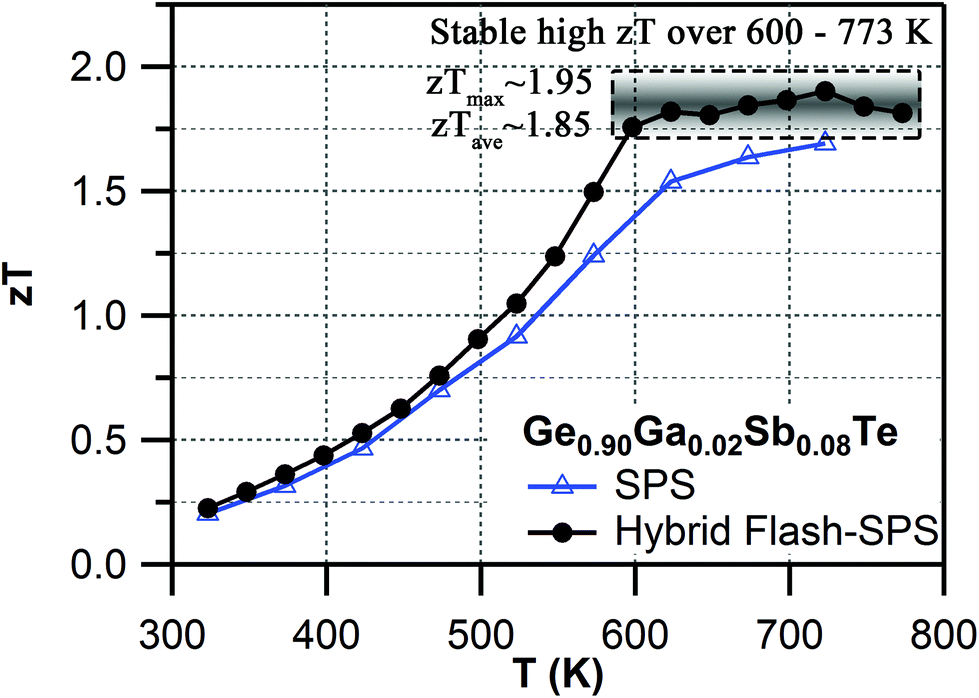 | ||
| Fig. 5 Temperature dependent zT for SPS vs. hybrid flash-SPS processed Ge0.90Ga0.02Sb0.08Te samples. | ||
4. Conclusion
In summary, on the basis of our experimental and theoretical studies, we conclude that the optimized codoping of Ga–Sb in c-GeTe induces multiple effects: (i) suppression of p-type charge carriers; (ii) activation of several bands with a larger effective mass in the transport; (iii) reduction of the structural transition temperature and enhancement of band degeneracy; (iv) convergence of light and heavy hole valence bands; (v) Ga contributes predominantly to the top of the valence band (and thus Ga together with Sb promoting band convergence), despite the Ga-induced resonance state not at a favorable position near the Fermi level. These cooperative (synergistic) effects, combined with the benefits of hybrid flash-SPS processing, i.e., improvement of thermopower and reduction of thermal transport without any degradation in carrier mobility, helped to achieve remarkably high and stabilized zT values (close to 2 for Ge0.90Ga0.02Sb0.08Te for instance, i.e. an improvement by 110% compared to undoped c-GeTe), making these Ga–Sb co-doped GeTe materials ideal candidates for mid-temperature power generation.Conflicts of interest
There are no conflicts to declare.Acknowledgements
The European Commission's Horizon 2020 research and innovation program under Marie Skłodowska-Curie GA.642557 (CoACH-ETN) is gratefully acknowledged for financial support. Dr Sylvain Tricot (IPR, Rennes) is acknowledged for his assistance in collecting Hall measurement data.References
- J. R. Sootsman, H. Kong, C. Uher, J. J. D'Angelo, C.-I. Wu, T. P. Hogan, T. Caillat and M. G. Kanatzidis, Angew. Chem., Int. Ed., 2008, 47, 8618–8622 CrossRef CAS PubMed.
- X. Su, P. Wei, H. Li, W. Liu, Y. Yan, P. Li, C. Su, C. Xie, W. Zhao, P. Zhai, Q. Zhang, X. Tang and C. Uher, Adv. Mater., 2017, 29, 1602013 CrossRef PubMed.
- Y. Zheng, Q. Zhang, X. Su, H. Xie, S. Shu, T. Chen, G. Tan, Y. Yan, X. Tang, C. Uher and G. J. Snyder, Adv. Energy Mater., 2015, 5, 1401391 CrossRef.
- D. T. Morelli, V. Jovovic and J. P. Heremans, Phys. Rev. Lett., 2008, 101, 035901 CrossRef CAS PubMed.
- M. K. Jana and K. Biswas, ACS Energy Lett., 2018, 3, 1315–1324 CrossRef CAS.
- M. Samanta, K. Pal, P. Pal, U. V. Waghmare and K. Biswas, J. Am. Chem. Soc., 2018, 140, 5866–5872 CrossRef CAS PubMed.
- B. C. Sales, D. Mandrus and R. K. Williams, Science, 1996, 272, 1325–1328 CrossRef CAS.
- A. Banik, U. S. Shenoy, S. Anand, U. V. Waghmare and K. Biswas, Chem. Mater., 2015, 27, 581–587 CrossRef CAS.
- Y. Pei, X. Shi, A. LaLonde, H. Wang, L. Chen and G. J. Snyder, Nature, 2011, 473, 66–69 CrossRef CAS PubMed.
- L. D. Hicks and M. S. Dresselhaus, Phys. Rev. B: Condens. Matter Mater. Phys., 1993, 47, 12727–12731 CrossRef CAS.
- J. M. O. Zide, D. Vashaee, Z. X. Bian, G. Zeng, J. E. Bowers, A. Shakouri and A. C. Gossard, Phys. Rev. B: Condens. Matter Mater. Phys., 2006, 74, 205335 CrossRef.
- Q. Zhang, B. Liao, Y. Lan, K. Lukas, W. Liu, K. Esfarjani, C. Opeil, D. Broido, G. Chen and Z. Ren, Proc. Natl. Acad. Sci. U. S. A., 2013, 110, 13261–13266 CrossRef CAS PubMed.
- S. Lin, W. Li, Z. Chen, J. Shen, B. Ge and Y. Pei, Nat. Commun., 2016, 7, 10287 CrossRef CAS.
- M. S. Dresselhaus, G. Chen, M. Y. Tang, R. G. Yang, H. Lee, D. Z. Wang, Z. F. Ren, J.-P. Fleurial and P. Gogna, Adv. Mater., 2007, 19, 1043–1053 CrossRef CAS.
- H. Wang, Y. Pei, A. D. LaLonde and G. J. Snyder, Proc. Natl. Acad. Sci. U. S. A, 2012, 109, 9705–9709 CrossRef CAS.
- Y. Pei, A. D. LaLonde, H. Wang and G. J. Snyder, Energy Environ. Sci., 2012, 5, 7963–7969 RSC.
- P. Lucas, C. Conseil, Z. Yang, Q. Hao, S. Cui, C. Boussard-Pledel, B. Bureau, F. Gascoin, C. Caillaud, O. Gulbiten, T. Guizouarn, P. Baruah, Q. Li and J. Lucas, J. Mater. Chem. A, 2013, 1, 8917–8925 RSC.
- B. Srinivasan, S. Cui, C. Prestipino, A. Gellé, C. Boussard-Pledel, S. Ababou-Girard, A. Trapananti, B. Bureau and S. Di Matteo, J. Phys. Chem. C, 2017, 121, 14045–14050 CrossRef CAS.
- B. Srinivasan, C. Boussard-Pledel, V. Dorcet, M. Samanta, K. Biswas, R. Lefèvre, F. Gascoin, F. Cheviré, S. Tricot, M. Reece and B. Bureau, Materials, 2017, 10, 328 CrossRef.
- A. P. Gonçalves, E. B. Lopes, G. Delaizir, J. B. Vaney, B. Lenoir, A. Piarristeguy, A. Pradel, J. Monnier, P. Ochin and C. Godart, J. Solid State Chem., 2012, 193, 26–30 CrossRef.
- R. Al Rahal Al Orabi, N. A. Mecholsky, J. Hwang, W. Kim, J.-S. Rhyee, D. Wee and M. Fornari, Chem. Mater., 2016, 28, 376–384 CrossRef CAS.
- A. Banik, U. S. Shenoy, S. Saha, U. V. Waghmare and K. Biswas, J. Am. Chem. Soc., 2016, 138, 13068–13075 CrossRef CAS PubMed.
- L. Wang, X. Tan, G. Liu, J. Xu, H. Shao, B. Yu, H. Jiang, S. Yue and J. Jiang, ACS Energy Lett., 2017, 2, 1203–1207 CrossRef.
- A. Banik, S. Roychowdhury and K. Biswas, Chem. Commun., 2018, 54, 6573–6590 RSC.
- B. Srinivasan, C. Boussard-Pledel and B. Bureau, Mater. Lett., 2018, 230, 191–194 CrossRef CAS.
- D. Bilc, S. D. Mahanti, E. Quarez, K.-F. Hsu, R. Pcionek and M. G. Kanatzidis, Phys. Rev. Lett., 2004, 93, 146403 CrossRef.
- Q. Zhang, F. Cao, W. Liu, K. Lukas, B. Yu, S. Chen, C. Opeil, D. Broido, G. Chen and Z. Ren, J. Am. Chem. Soc., 2012, 134, 10031–10038 CrossRef CAS PubMed.
- B. Srinivasan, F. Gucci, C. Boussard-Pledel, F. Cheviré, M. J. Reece, S. Tricot, L. Calvez and B. Bureau, J. Alloys Compd., 2017, 729, 198–202 CrossRef CAS.
- C. Fu, S. Bai, Y. Liu, Y. Tang, L. Chen, X. Zhao and T. Zhu, Nat. Commun., 2015, 6, 8144 CrossRef.
- W. Liu, X. Tan, K. Yin, H. Liu, X. Tang, J. Shi, Q. Zhang and C. Uher, Phys. Rev. Lett., 2012, 108, 166601 CrossRef.
- S. H. Yang, T. J. Zhu, T. Sun, J. He, S. N. Zhang and X. B. Zhao, Nanotechnology, 2008, 19, 245707 CrossRef CAS.
- T. Schröder, S. Schwarzmüller, C. Stiewe, J. de Boor, M. Hölzel and O. Oeckler, Inorg. Chem., 2013, 52, 11288–11294 CrossRef PubMed.
- T. Schröder, T. Rosenthal, N. Giesbrecht, S. Maier, E.-W. Scheidt, W. Scherer, G. J. Snyder, W. Schnick and O. Oeckler, J. Mater. Chem. A, 2014, 2, 6384–6395 RSC.
- M. Samanta, S. Roychowdhury, J. Ghatak, S. Perumal and K. Biswas, Chem. – Eur. J., 2017, 23, 7438–7443 CrossRef CAS.
- F. Fahrnbauer, D. Souchay, G. Wagner and O. Oeckler, J. Am. Chem. Soc., 2015, 137, 12633–12638 CrossRef CAS.
- Y. Gelbstein and J. Davidow, Phys. Chem. Chem. Phys., 2014, 16, 20120–20126 RSC.
- S. Perumal, S. Roychowdhury and K. Biswas, Inorg. Chem. Front., 2016, 3, 125–132 RSC.
- D. Wu, L.-D. Zhao, S. Hao, Q. Jiang, F. Zheng, J. W. Doak, H. Wu, H. Chi, Y. Gelbstein, C. Uher, C. Wolverton, M. Kanatzidis and J. He, J. Am. Chem. Soc., 2014, 136, 11412–11419 CrossRef CAS.
- L. Wu, X. Li, S. Wang, T. Zhang, J. Yang, W. Zhang, L. Chen and J. Yang, NPG Asia Mater., 2017, 9, e343 CrossRef CAS.
- L. Yang, J. Q. Li, R. Chen, Y. Li, F. S. Liu and W. Q. Ao, J. Electron. Mater., 2016, 45, 5533–5539 CrossRef CAS.
- S. Perumal, S. Roychowdhury, D. S. Negi, R. Datta and K. Biswas, Chem. Mater., 2015, 27, 7171–7178 CrossRef CAS.
- E. Nshimyimana, X. Su, H. Xie, W. Liu, R. Deng, T. Luo, Y. Yan and X. Tang, Sci. Bull., 2018, 63, 717–725 CrossRef CAS.
- B. Srinivasan, R. Gautier, F. Gucci, B. Fontaine, J.-F. Halet, F. Cheviré, C. Boussard-Pledel, M. J. Reece and B. Bureau, J. Phys. Chem. C, 2018, 122, 227–235 CrossRef CAS.
- Z. Zheng, X. Su, R. Deng, C. Stoumpos, H. Xie, W. Liu, Y. Yan, S. Hao, C. Uher, C. Wolverton, M. G. Kanatzidis and X. Tang, J. Am. Chem. Soc., 2018, 140, 2673–2686 CrossRef CAS PubMed.
- J. K. Lee, M. W. Oh, B. S. Kim, B. K. Min, H. W. Lee and S. D. Park, Electron. Mater. Lett., 2014, 10, 813–817 CrossRef CAS.
- Y. Rosenberg, Y. Gelbstein and M. P. Dariel, J. Alloys Compd., 2012, 526, 31–38 CrossRef CAS.
- J. Li, X. Zhang, S. Lin, Z. Chen and Y. Pei, Chem. Mater., 2017, 29, 605–611 CrossRef CAS.
- M. Samanta and K. Biswas, J. Am. Chem. Soc., 2017, 139, 9382–9391 CrossRef CAS.
- S. Perumal, P. Bellare, U. S. Shenoy, U. V. Waghmare and K. Biswas, Chem. Mater., 2017, 29, 10426–10435 CrossRef CAS.
- J. Li, X. Zhang, Z. Chen, S. Lin, W. Li, J. Shen, I. T. Witting, A. Faghaninia, Y. Chen, A. Jain, L. Chen, G. J. Snyder and Y. Pei, Joule, 2018, 2, 976–987 CrossRef CAS.
- S. Perumal, S. Roychowdhury and K. Biswas, J. Mater. Chem. C, 2016, 4, 7520–7536 RSC.
- F. Gucci, T. G. Saunders and M. J. Reece, Scr. Mater., 2018, 157, 58–61 CrossRef CAS.
- B. Srinivasan, B. Fontaine, F. Gucci, V. Dorcet, T. G. Saunders, M. Yu, F. Cheviré, C. Boussard-Pledel, J.-F. Halet, R. Gautier, M. J. Reece and B. Bureau, Inorg. Chem., 2018, 57, 12976–12986 CrossRef CAS.
- H.-S. Kim, Z. M. Gibbs, Y. Tang, H. Wang and G. J. Snyder, APL Mater., 2015, 3, 041506 CrossRef.
- L. Zhang, J. Wang, Z. Cheng, Q. Sun, Z. Li and S. Dou, J. Mater. Chem. A, 2016, 4, 7936–7942 RSC.
- G. Kresse and D. Joubert, Phys. Rev. B: Condens. Matter Mater. Phys., 1999, 59, 1758–1775 CrossRef CAS.
- G. Kresse and J. Furthmüller, Phys. Rev. B: Condens. Matter Mater. Phys., 1996, 54, 11169–11186 CrossRef CAS.
- J. P. Perdew, K. Burke and M. Ernzerhof, Phys. Rev. Lett., 1996, 77, 3865–3868 CrossRef CAS.
- K. Hoang, S. D. Mahanti and M. G. Kanatzidis, Phys. Rev. B: Condens. Matter Mater. Phys., 2010, 81, 115106 CrossRef.
- A. F. May, E. S. Toberer, A. Saramat and G. J. Snyder, Phys. Rev. B: Condens. Matter Mater. Phys., 2009, 80, 125205 CrossRef.
- E. S. Toberer, A. Zevalkink, N. Crisosto and G. J. Snyder, Adv. Funct. Mater., 2010, 20, 4375–4380 CrossRef CAS.
- E. M. Levin, M. F. Besser and R. Hanus, J. Appl. Phys., 2013, 114, 083713 CrossRef.
- E. M. Levin, Phys. Rev. B: Condens. Matter Mater. Phys., 2016, 93, 045209 CrossRef.
- J. Androulakis, I. Todorov, D.-Y. Chung, S. Ballikaya, G. Wang, C. Uher and M. Kanatzidis, Phys. Rev. B: Condens. Matter Mater. Phys., 2010, 82, 115209 CrossRef.
- S. Roychowdhury, U. Sandhya Shenoy, U. V. Waghmare and K. Biswas, J. Mater. Chem. C, 2017, 5, 5737–5748 RSC.
- M. Hong, Z.-G. Chen, L. Yang, Y.-C. Zou, M. S. Dargusch, H. Wang and J. Zou, Adv. Mater., 2018, 30, 1705942 CrossRef.
- H. Fritzsche, Science, 1972, 176, 1117–1117 CrossRef.
- B. Du, F. Gucci, H. Porwal, S. Grasso, A. Mahajan and M. J. Reece, J. Mater. Chem. C, 2017, 5, 1514–1521 RSC.
- M. Cologna, B. Rashkova and R. Raj, J. Am. Ceram. Soc., 2010, 93, 3556–3559 CrossRef CAS.
- M. Yu, S. Grasso, R. Mckinnon, T. Saunders and M. J. Reece, Adv. Appl. Ceram., 2017, 116, 24–60 CrossRef CAS.
- E. A. Olevsky, S. M. Rolfing and A. L. Maximenko, Sci. Rep., 2016, 6, 33408 CrossRef CAS.
- S. Grasso, E.-Y. Kim, T. Saunders, M. Yu, A. Tudball, S.-H. Choi and M. Reece, Cryst. Growth Des., 2016, 16, 2317–2321 CrossRef CAS.
- S. Grasso, T. Saunders, H. Porwal, O. Cedillos-Barraza, D. D. Jayaseelan, W. E. Lee, M. J. Reece and W. Fahrenholtz, J. Am. Ceram. Soc., 2014, 97, 2405–2408 CrossRef CAS.
- J. L. Wang, H. Wang, G. J. Snyder, X. Zhang, Z. H. Ni and Y. F. Chen, J. Phys. D: Appl. Phys., 2013, 46, 405301 CrossRef.
Footnote |
| † Electronic supplementary information (ESI) available. See DOI: 10.1039/c8qi00703a |
| This journal is © the Partner Organisations 2019 |